75124267e4d36a48161f58b9251f14da.ppt
- Количество слайдов: 47
 Power. Point Overheads for Sedra/Smith Microelectronic Circuits 5/e Microelectronic Circuits - Fifth Edition Sedra/Smith © 2004 Oxford University Press. 1
 u Microelectronics refers to the integrated circuit (IC) technology. producing circuits that contains millions components in a silicon chip (100 mm 2). Ex) microprocessor u In this semester, we shall study - electronics that can be used singly (in the design of discrete circuits) as components of an integrated-circuit (IC) chip. - the design and analysis of interconnection of these devices. - available IC chips and their applications in the design of electronic system. Microelectronic Circuits - Fifth Edition Sedra/Smith Copyright 2004 by Oxford University Press, Inc. 2
 Part I Devices and Basic Circuits The most fundamental and essential topics for the study of electronic circuits. Chap. 1: Introduction to Electronics Chap. 2: Operational Amplifier* Chap. 3: Diode Chap. 4: MOS Field-Effect Transistors (MOSFETs) Chap. 5: Bipolar Junction Transistor (BJTs) * Op amp is, strictly speaking, not an basic electronic device. Op amp’s internal circuit is complex (20 or more transistors). Why we should study the op amps here? Op amp is commercially available as an integrated circuit (IC) package. Op amp has well-defined terminal characteristics. Microelectronic Circuits - Fifth Edition Sedra/Smith ? 3
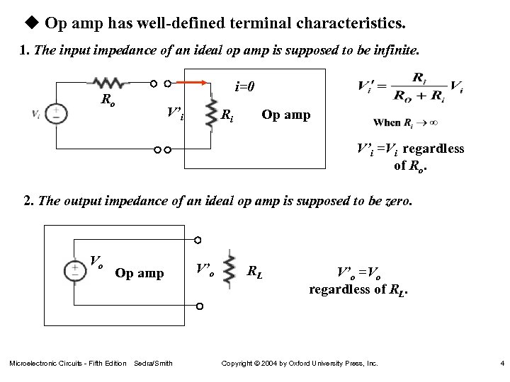 u Op amp has well-defined terminal characteristics. 1. The input impedance of an ideal op amp is supposed to be infinite. i=0 Ro V’i Ri Op amp V’i =Vi regardless of Ro. 2. The output impedance of an ideal op amp is supposed to be zero. Vo Op amp Microelectronic Circuits - Fifth Edition Sedra/Smith V’o RL V’o =Vo regardless of RL. Copyright 2004 by Oxford University Press, Inc. 4
 Introduction to Electronics u The purpose of this chapter To introduce some basic concept and terminology. Signals Signal amplification Models for linear amplifier Digital logic inverters Circuit simulation using SPICE Microelectronic Circuits - Fifth Edition Sedra/Smith 5
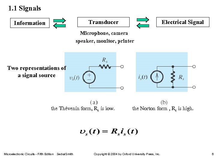 1. 1 Signals Transducer Information Electrical Signal Microphone, camera speaker, monitor, printer Two representations of a signal source the Thévenin form, Rs is low. Microelectronic Circuits - Fifth Edition Sedra/Smith the Norton form , Rs is high. Copyright 2004 by Oxford University Press, Inc. 6
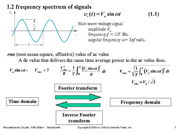 1. 2 frequency spectrum of signals Sine-wave voltage signal amplitude Va frequency f = 1/T Hz. angular frequency ω = 2πf rad/s. rms (root-mean-square, effective) value of ac value A dc value that delivers the same time average power as the ac value does. Fourier transform Time domain Frequency domain Inverse Fourier transform Microelectronic Circuits - Fifth Edition Sedra/Smith Copyright 2004 by Oxford University Press, Inc. 7
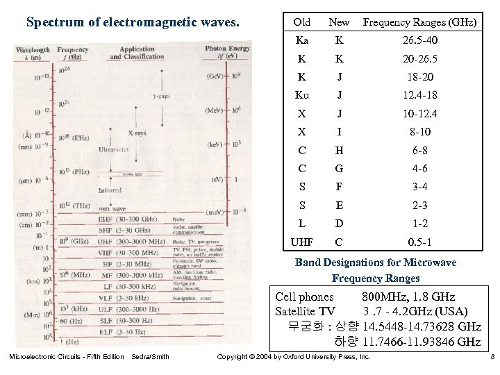 Spectrum of electromagnetic waves. Old New Frequency Ranges (GHz) Ka K 26. 5 -40 K K 20 -26. 5 K J 18 -20 Ku J 12. 4 -18 X J 10 -12. 4 X I 8 -10 C H 6 -8 C G 4 -6 S F 3 -4 S E 2 -3 L D 1 -2 UHF C 0. 5 -1 Band Designations for Microwave Frequency Ranges Cell phones 800 MHz, 1. 8 GHz Satellite TV 3. 7 - 4. 2 GHz (USA) 무궁화 : 상향 14. 5448 -14. 73628 GHz 하향 11. 7466 -11. 93846 GHz Microelectronic Circuits - Fifth Edition Sedra/Smith Copyright 2004 by Oxford University Press, Inc. 8
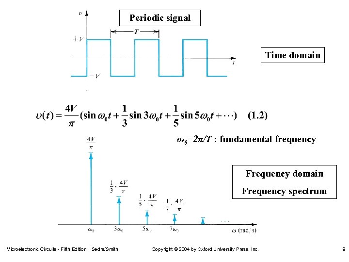 Periodic signal Time domain ω0=2π/T : fundamental frequency Frequency domain Frequency spectrum Microelectronic Circuits - Fifth Edition Sedra/Smith Copyright 2004 by Oxford University Press, Inc. 9
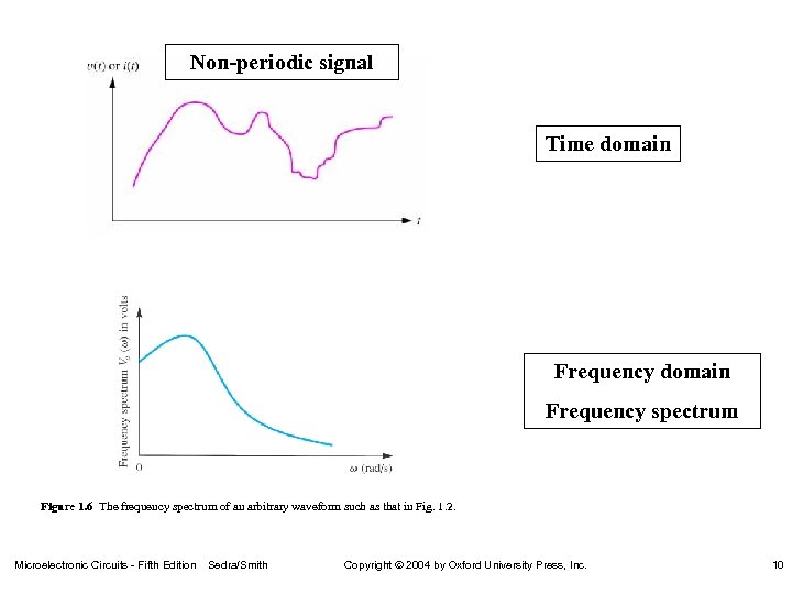 Non-periodic signal Time domain Frequency spectrum Figure 1. 6 The frequency spectrum of an arbitrary waveform such as that in Fig. 1. 2. Microelectronic Circuits - Fifth Edition Sedra/Smith Copyright 2004 by Oxford University Press, Inc. 10
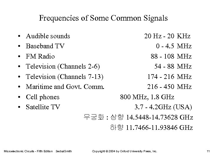 Frequencies of Some Common Signals • • Audible sounds 20 Hz - 20 KHz Baseband TV 0 - 4. 5 MHz FM Radio 88 - 108 MHz Television (Channels 2 -6) 54 - 88 MHz Television (Channels 7 -13) 174 - 216 MHz Maritime and Govt. Comm. 216 - 450 MHz Cell phones 800 MHz, 1. 8 GHz Satellite TV 3. 7 - 4. 2 GHz (USA) 무궁화 : 상향 14. 5448 -14. 73628 GHz 하향 11. 7466 -11. 93846 GHz Microelectronic Circuits - Fifth Edition Sedra/Smith Copyright 2004 by Oxford University Press, Inc. 11
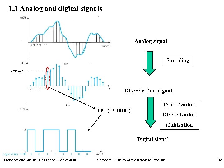 1. 3 Analog and digital signals Analog signal Sampling 180 m. V Discrete-time signal 180=(10110100) Quantization Discretization digitization Digital signal Microelectronic Circuits - Fifth Edition Sedra/Smith Copyright 2004 by Oxford University Press, Inc. 12
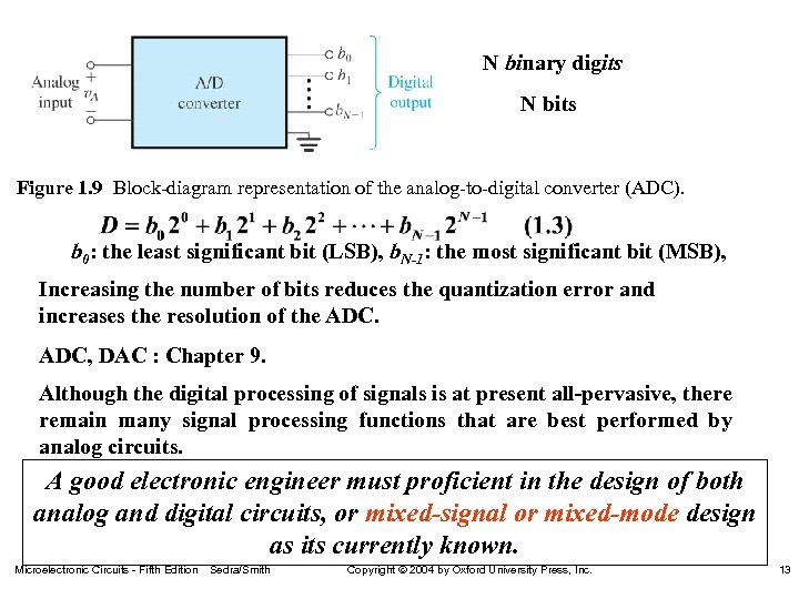 N binary digits N bits Figure 1. 9 Block-diagram representation of the analog-to-digital converter (ADC). b 0: the least significant bit (LSB), b. N-1: the most significant bit (MSB), Increasing the number of bits reduces the quantization error and increases the resolution of the ADC, DAC : Chapter 9. Although the digital processing of signals is at present all-pervasive, there remain many signal processing functions that are best performed by analog circuits. A good electronic engineer must proficient in the design of both analog and digital circuits, or mixed-signal or mixed-mode design as its currently known. Microelectronic Circuits - Fifth Edition Sedra/Smith Copyright 2004 by Oxford University Press, Inc. 13
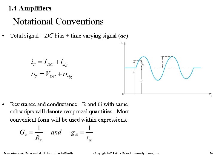 1. 4 Amplifiers Notational Conventions • Total signal = DC bias + time varying signal (ac) • Resistance and conductance - R and G with same subscripts will denote reciprocal quantities. Most convenient form will be used within expressions. Microelectronic Circuits - Fifth Edition Sedra/Smith Copyright 2004 by Oxford University Press, Inc. 14
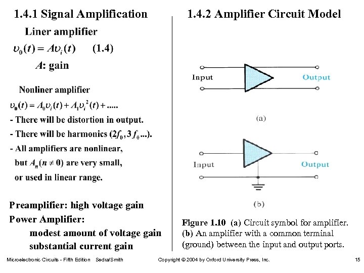 1. 4. 1 Signal Amplification 1. 4. 2 Amplifier Circuit Model Preamplifier: high voltage gain Power Amplifier: modest amount of voltage gain substantial current gain Microelectronic Circuits - Fifth Edition Sedra/Smith Figure 1. 10 (a) Circuit symbol for amplifier. (b) An amplifier with a common terminal (ground) between the input and output ports. Copyright 2004 by Oxford University Press, Inc. 15
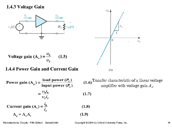 1. 4. 3 Voltage Gain 1. 4. 4 Power Gain and Current Gain Transfer characteristic of a linear voltage amplifier with voltage gain Av. Microelectronic Circuits - Fifth Edition Sedra/Smith Copyright 2004 by Oxford University Press, Inc. 16
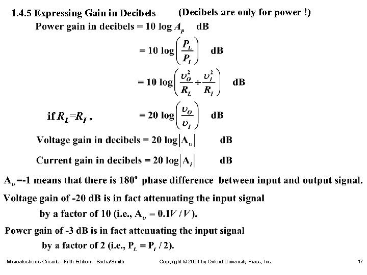 1. 4. 5 Expressing Gain in Decibels (Decibels are only for power !) if RL=RI , Microelectronic Circuits - Fifth Edition Sedra/Smith Copyright 2004 by Oxford University Press, Inc. 17
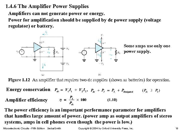 1. 4. 6 The Amplifier Power Supplies Amplifiers can not generate power or energy. Power for amplification should be supplied by dc power supply (voltage regulator) or battery. Some amps use only one power supply. Figure 1. 12 An amplifier that requires two dc supplies (shown as batteries) for operation. Energy conservation Amplifier efficiency The power efficiency is an important performance parameter for amplifiers that handles large amount of power. (power amp as output amplifiers of stereo systems, amps in cell phones even though the power is low. ) Microelectronic Circuits - Fifth Edition Sedra/Smith Copyright 2004 by Oxford University Press, Inc. 18
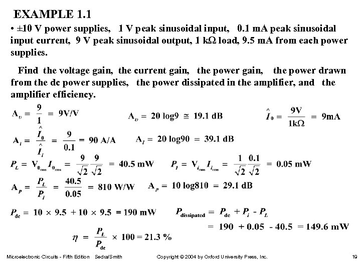 EXAMPLE 1. 1 • ± 10 V power supplies, 1 V peak sinusoidal input, 0. 1 m. A peak sinusoidal input current, 9 V peak sinusoidal output, 1 kΩ load, 9. 5 m. A from each power supplies. Find the voltage gain, the current gain, the power drawn from the dc power supplies, the power dissipated in the amplifier, and the amplifier efficiency. Microelectronic Circuits - Fifth Edition Sedra/Smith Copyright 2004 by Oxford University Press, Inc. 19
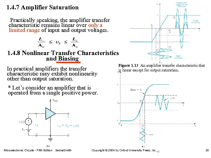 1. 4. 7 Amplifier Saturation Practically speaking, the amplifier transfer characteristic remains linear over only a limited range of input and output voltages. 1. 4. 8 Nonlinear Transfer Characteristics and Biasing In practical amplifiers the transfer characteristic may exhibit nonlinearity other than output saturation. Figure 1. 13 An amplifier transfer characteristic that is linear except for output saturation. * Let’s consider an amplifier that is operated from a single positive power. Microelectronic Circuits - Fifth Edition Sedra/Smith Copyright 2004 by Oxford University Press, Inc. 20
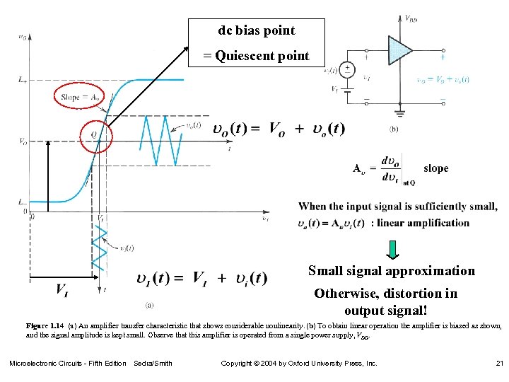 dc bias point = Quiescent point Small signal approximation Otherwise, distortion in output signal! Figure 1. 14 (a) An amplifier transfer characteristic that shows considerable nonlinearity. (b) To obtain linear operation the amplifier is biased as shown, and the signal amplitude is kept small. Observe that this amplifier is operated from a single power supply, VDD. Microelectronic Circuits - Fifth Edition Sedra/Smith Copyright 2004 by Oxford University Press, Inc. 21
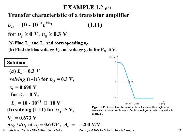 EXAMPLE 1. 2 p 21 (a) Find L_ and L+ and corresponding υI. (b) Find dc bias voltage VI and voltage gain for VO=5 V. Solution Figure 1. 15 A sketch of the transfer characteristic of the amplifier of Example 1. 2. Note that this amplifier is inverting (i. e. , with a gain that is negative). Microelectronic Circuits - Fifth Edition Sedra/Smith Copyright 2004 by Oxford University Press, Inc. 22
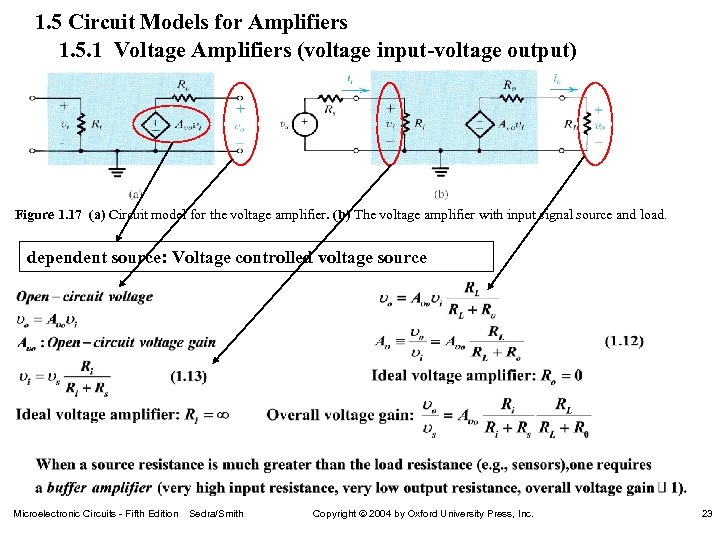 1. 5 Circuit Models for Amplifiers 1. 5. 1 Voltage Amplifiers (voltage input-voltage output) Figure 1. 17 (a) Circuit model for the voltage amplifier. (b) The voltage amplifier with input signal source and load. dependent source: Voltage controlled voltage source Microelectronic Circuits - Fifth Edition Sedra/Smith Copyright 2004 by Oxford University Press, Inc. 23
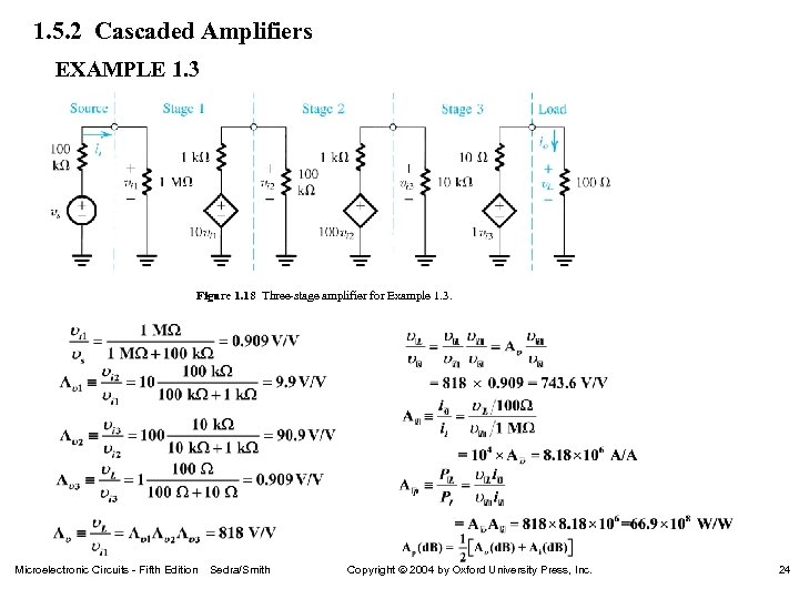 1. 5. 2 Cascaded Amplifiers EXAMPLE 1. 3 Figure 1. 18 Three-stage amplifier for Example 1. 3. Microelectronic Circuits - Fifth Edition Sedra/Smith Copyright 2004 by Oxford University Press, Inc. 24
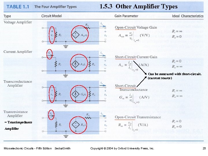 1. 5. 3 Other Amplifier Types Can be measured with short-circuit. (current source) = Transimpedance Amplifier Microelectronic Circuits - Fifth Edition Sedra/Smith Copyright 2004 by Oxford University Press, Inc. 25
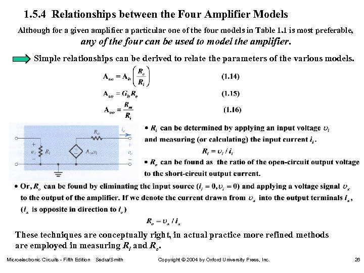 1. 5. 4 Relationships between the Four Amplifier Models Although for a given amplifier a particular one of the four models in Table 1. 1 is most preferable, any of the four can be used to model the amplifier. Simple relationships can be derived to relate the parameters of the various models. These techniques are conceptually right, in actual practice more refined methods are employed in measuring Ri and Ro. Microelectronic Circuits - Fifth Edition Sedra/Smith Copyright 2004 by Oxford University Press, Inc. 26
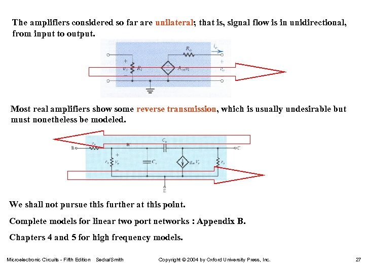 The amplifiers considered so far are unilateral; that is, signal flow is in unidirectional, from input to output. Most real amplifiers show some reverse transmission, which is usually undesirable but must nonetheless be modeled. We shall not pursue this further at this point. Complete models for linear two port networks : Appendix B. Chapters 4 and 5 for high frequency models. Microelectronic Circuits - Fifth Edition Sedra/Smith Copyright 2004 by Oxford University Press, Inc. 27
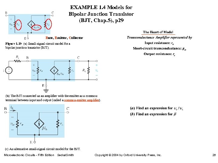 EXAMPLE 1. 4 Models for Bipolar Junction Transistor (BJT, Chap. 5), p 29 Base, Emitter, Collector Figure 1. 19 (a) Small-signal circuit model for a bipolar junction transistor (BJT). (b) The BJT connected as an amplifier with the emitter as a common terminal between input and output (called a common-emitter amplifier). (c) An alternative small-signal circuit model for the BJT. Microelectronic Circuits - Fifth Edition Sedra/Smith Copyright 2004 by Oxford University Press, Inc. 28
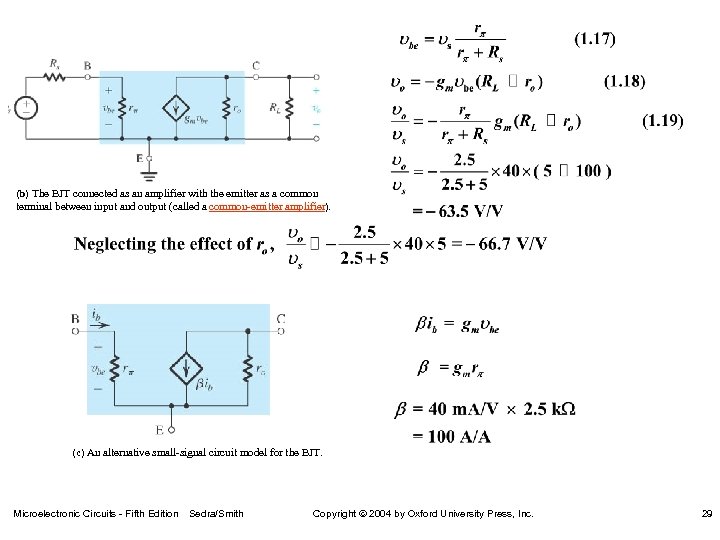 (b) The BJT connected as an amplifier with the emitter as a common terminal between input and output (called a common-emitter amplifier). (c) An alternative small-signal circuit model for the BJT. Microelectronic Circuits - Fifth Edition Sedra/Smith Copyright 2004 by Oxford University Press, Inc. 29
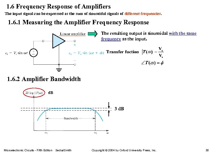 1. 6 Frequency Response of Amplifiers The input signal can be expressed as the sum of sinusoidal signals of different frequencies. 1. 6. 1 Measuring the Amplifier Frequency Response The resulting output is sinusoidal with the same frequency as the input. 1. 6. 2 Amplifier Bandwidth d. B 3 d. B Microelectronic Circuits - Fifth Edition Sedra/Smith Copyright 2004 by Oxford University Press, Inc. 30
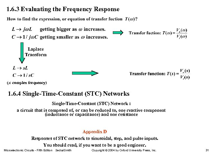 1. 6. 3 Evaluating the Frequency Response Laplace Transform (s: complex frequency) 1. 6. 4 Single-Time-Constant (STC) Networks Single-Time-Constant (STC) Network : a circuit that is composed of, or can be reduced to, one reactive component (inductance or capacitance) and one resistance Appendix D Responses of STC network to sinusoidal, step, and pulse inputs. You should read, if you want to be a good engineer. Microelectronic Circuits - Fifth Edition Sedra/Smith Copyright 2004 by Oxford University Press, Inc. 31
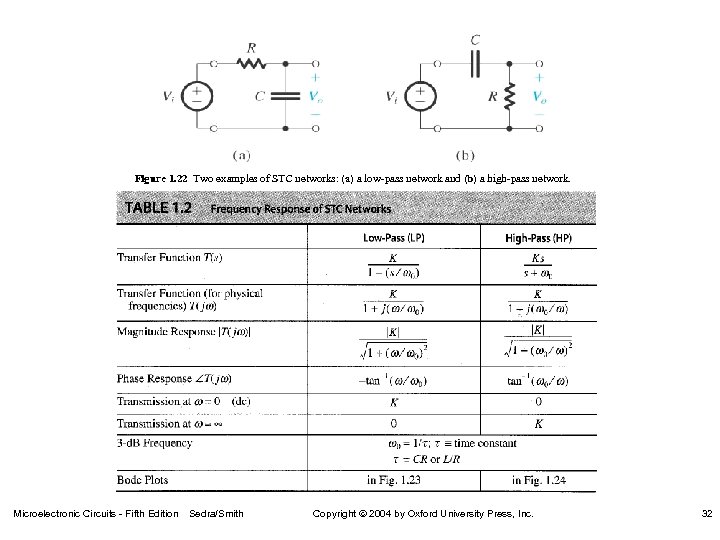 Figure 1. 22 Two examples of STC networks: (a) a low-pass network and (b) a high-pass network. Microelectronic Circuits - Fifth Edition Sedra/Smith Copyright 2004 by Oxford University Press, Inc. 32
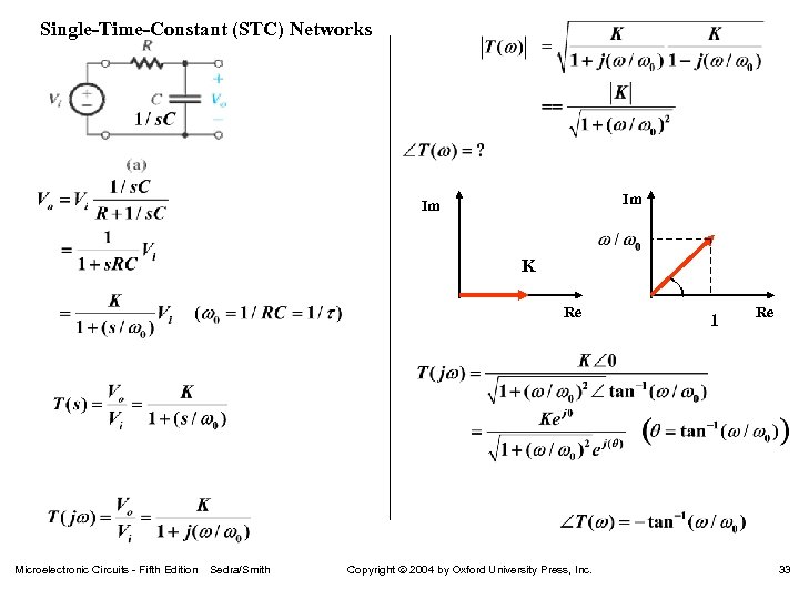 Single-Time-Constant (STC) Networks Im Im K Re Microelectronic Circuits - Fifth Edition Sedra/Smith Copyright 2004 by Oxford University Press, Inc. 1 Re 33
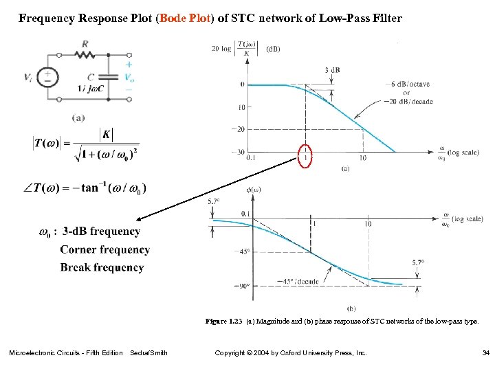 Frequency Response Plot (Bode Plot) of STC network of Low-Pass Filter Figure 1. 23 (a) Magnitude and (b) phase response of STC networks of the low-pass type. Microelectronic Circuits - Fifth Edition Sedra/Smith Copyright 2004 by Oxford University Press, Inc. 34
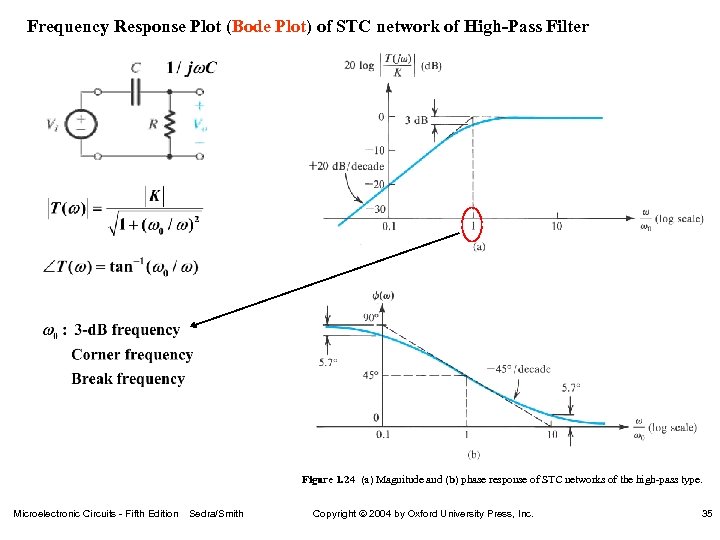 Frequency Response Plot (Bode Plot) of STC network of High-Pass Filter Figure 1. 24 (a) Magnitude and (b) phase response of STC networks of the high-pass type. Microelectronic Circuits - Fifth Edition Sedra/Smith Copyright 2004 by Oxford University Press, Inc. 35
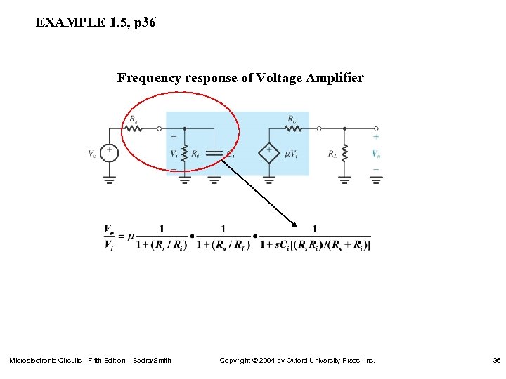 EXAMPLE 1. 5, p 36 Frequency response of Voltage Amplifier Microelectronic Circuits - Fifth Edition Sedra/Smith Copyright 2004 by Oxford University Press, Inc. 36
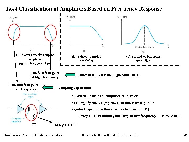 1. 6. 4 Classification of Amplifiers Based on Frequency Response (a) a capacitively coupled amplifier Ex) Audio Amplifier (b) a direct-coupled amplifier The falloff of gain at high frequency The falloff of gain at low frequency (c) a tuned or bandpass amplifier. Internal capacitance Ci (previous slide) Coupling capacitance • Used to connect one amplifier to another • to simplify the design process of different amplifier • Quite large ( a fraction of μF ~a few tens of μF ) – very small reactance, but large at low frequency → voltage drop High-pass STC Microelectronic Circuits - Fifth Edition Sedra/Smith Copyright 2004 by Oxford University Press, Inc. 37
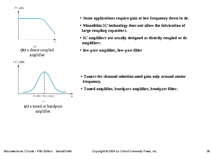 • Some applications require gain at low frequency down to dc. • Monolithic IC technology does not allow the fabrication of large coupling capacitors. • IC amplifiers are usually designed as directly coupled or dc amplifiers. (b) a direct-coupled amplifier • low-pass amplifier, low-pass filter • Tuners for channel selection need gain only around center frequency. • Tuned amplifier, bandpass filter. (c) a tuned or bandpass amplifier. Microelectronic Circuits - Fifth Edition Sedra/Smith Copyright 2004 by Oxford University Press, Inc. 38
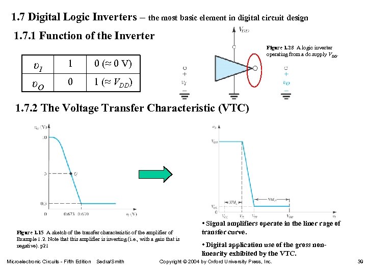 1. 7 Digital Logic Inverters – the most basic element in digital circuit design 1. 7. 1 Function of the Inverter υI υO 1 0 (≈ 0 V) 0 Figure 1. 28 A logic inverter operating from a dc supply VDD. 1 (≈ VDD) 1. 7. 2 The Voltage Transfer Characteristic (VTC) Figure 1. 15 A sketch of the transfer characteristic of the amplifier of Example 1. 2. Note that this amplifier is inverting (i. e. , with a gain that is negative). p 21 Microelectronic Circuits - Fifth Edition Sedra/Smith • Signal amplifiers operate in the liner rage of transfer curve. • Digital application use of the gross nonlinearity exhibited by the VTC. Copyright 2004 by Oxford University Press, Inc. 39
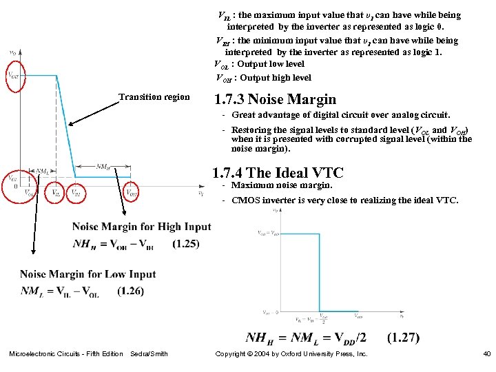 VIL : the maximum input value that υI can have while being interpreted by the inverter as represented as logic 0. VIH : the minimum input value that υI can have while being interpreted by the inverter as represented as logic 1. VOL : Output low level VOH : Output high level Transition region 1. 7. 3 Noise Margin - Great advantage of digital circuit over analog circuit. - Restoring the signal levels to standard level (VOL and VOH) when it is presented with corrupted signal level (within the noise margin). 1. 7. 4 The Ideal VTC - Maximum noise margin. - CMOS inverter is very close to realizing the ideal VTC. Microelectronic Circuits - Fifth Edition Sedra/Smith Copyright 2004 by Oxford University Press, Inc. 40
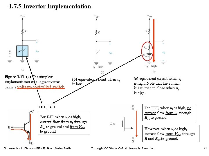 1. 7. 5 Inverter Implementation Figure 1. 31 (a) The simplest implementation of a logic inverter using a voltage-controlled switch (b) equivalent circuit when υI is low FET, BJT For BJT, when υI is high, current flow from υI through Ron to ground and from VDD to ground Microelectronic Circuits - Fifth Edition Sedra/Smith (c) equivalent circuit when υI is high. Note that the switch is assumed to close when υI is high. For FET, when υI is high, no current flow from υI through Ron to ground. However, when υI is high, current flow from VDD through R and Ron to ground. Copyright 2004 by Oxford University Press, Inc. 41
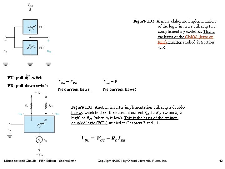 Figure 1. 32 A more elaborate implementation of the logic inverter utilizing two complementary switches. This is the basis of the CMOS (base on FET) inverter studied in Section 4. 10. PU: pull-up switch PD: pull-down switch VOH = VDD VOL = 0 No current flows! Figure 1. 33 Another inverter implementation utilizing a doublethrow switch to steer the constant current IEE to RC 1 (when υI is high) or RC 2 (when υI is low). This is the basis of the emittercoupled logic (ECL) studied in Chapters 7 and 11. Microelectronic Circuits - Fifth Edition Sedra/Smith Copyright 2004 by Oxford University Press, Inc. 42
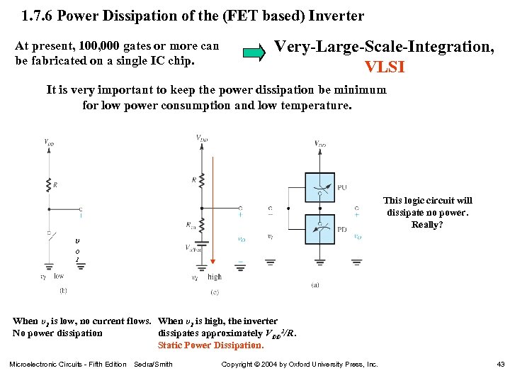 1. 7. 6 Power Dissipation of the (FET based) Inverter At present, 100, 000 gates or more can be fabricated on a single IC chip. Very-Large-Scale-Integration, VLSI It is very important to keep the power dissipation be minimum for low power consumption and low temperature. This logic circuit will dissipate no power. Really? υ O 1 When υI is low, no current flows. When υI is high, the inverter No power dissipation dissipates approximately VDD 2/R. Static Power Dissipation. Microelectronic Circuits - Fifth Edition Sedra/Smith Copyright 2004 by Oxford University Press, Inc. 43
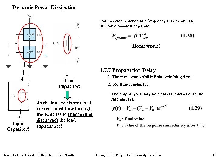 Dynamic Power Dissipation An inverter switched at a frequency f Hz exhibits a dynamic power dissipation, Homework! 1. 7. 7 Propagation Delay Load Capacitor! Input Capacitor! As the inverter is switched, current must flow through the switches to charge (and discharge) the load capacitance! Microelectronic Circuits - Fifth Edition Sedra/Smith 1. The transistors exhibit finite switching times. 2. RC time constant τ. The output y(t) at any time t of STC network to the step input is, Copyright 2004 by Oxford University Press, Inc. 44
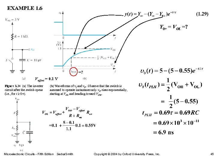 EXAMPLE 1. 6 Y 0+ = VOL =? Voffset = 0. 1 V Figure 1. 34 (a) The inverter circuit after the switch opens (i. e. , for t 0 ). (b) Waveforms of v. I and v. O. Observe that the switch is assumed to operate instantaneously. v. O rises exponentially, starting at VOL and heading toward VOH. Microelectronic Circuits - Fifth Edition Sedra/Smith Copyright 2004 by Oxford University Press, Inc. 45
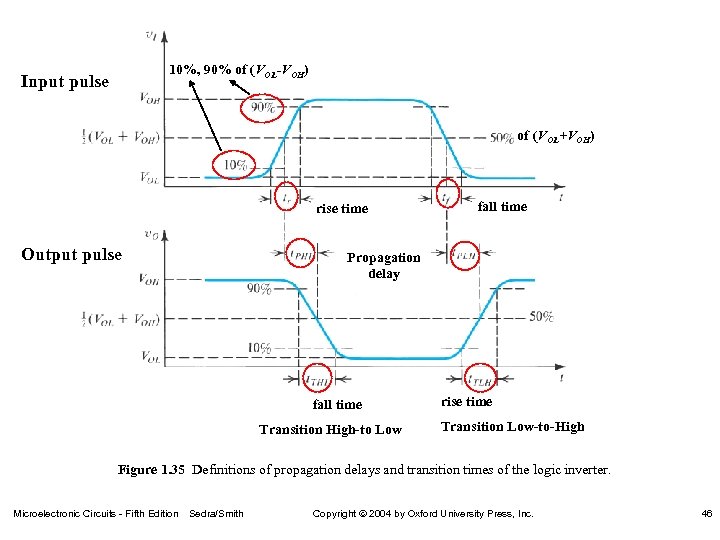 10%, 90% of (VOL-VOH) Input pulse of (VOL+VOH) rise time Output pulse fall time Propagation delay fall time Transition High-to Low rise time Transition Low-to-High Figure 1. 35 Definitions of propagation delays and transition times of the logic inverter. Microelectronic Circuits - Fifth Edition Sedra/Smith Copyright 2004 by Oxford University Press, Inc. 46
 1. 8 Circuit Simulation Using SPICE (Simulation Program with Integrated Circuit Emphasis) The use of computer programs to simulate the operation of electronic circuits has become an essential in the circuit-build process before step and after fabrication. • Circuit simulation enables the designer; - To verify the design to meet specification when actual components (with their many imperfection) are used. - To get additional insight into circuit operation. - To fine-tune the final design prior to fabrication. It is not a substitute for a thorough understanding of circuit operation ! It should be performed only a later stage in the design process after a paper-and-pencil design has been done ! • PSpice is a commercial PC version of SPICE (Cadence). • PSpice A/D : analog and digital signal • Or. CAD Capture CIS (Component Information System) : graphical interface ( referred in this book) Microelectronic Circuits - Fifth Edition Sedra/Smith Copyright 2004 by Oxford University Press, Inc. 47


