d878bc836016cb8971a07fc3b266d33d.ppt
- Количество слайдов: 38
 PID Electronics ETD meeting Electronic design for the barrel : Front end chip and TDC (one talk) Forward PID electronics ( two talks ) Next steps and millestones On behalf of PID group Dec 16 2010 Christophe Beigbeder ETD meeting 1
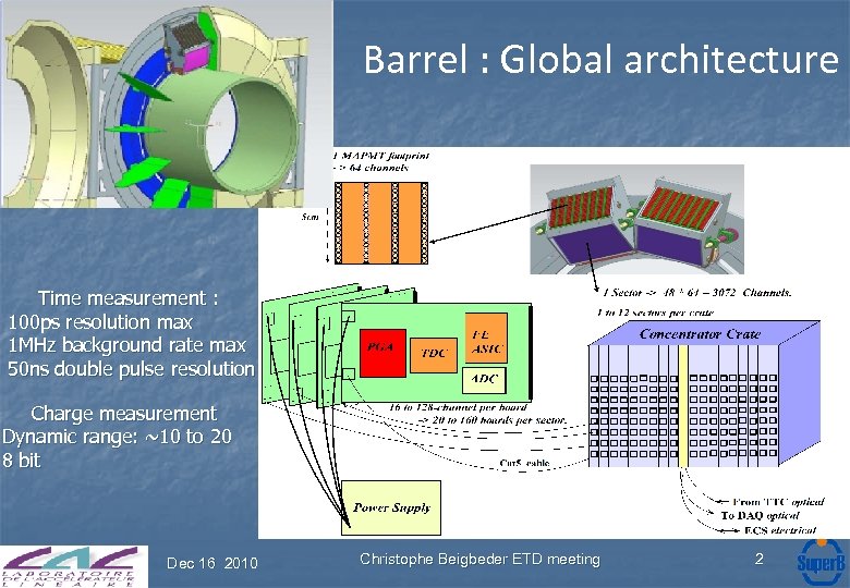 Barrel : Global architecture Time measurement : 100 ps resolution max 1 MHz background rate max 50 ns double pulse resolution Charge measurement Dynamic range: ~10 to 20 8 bit Dec 16 2010 Christophe Beigbeder ETD meeting 2
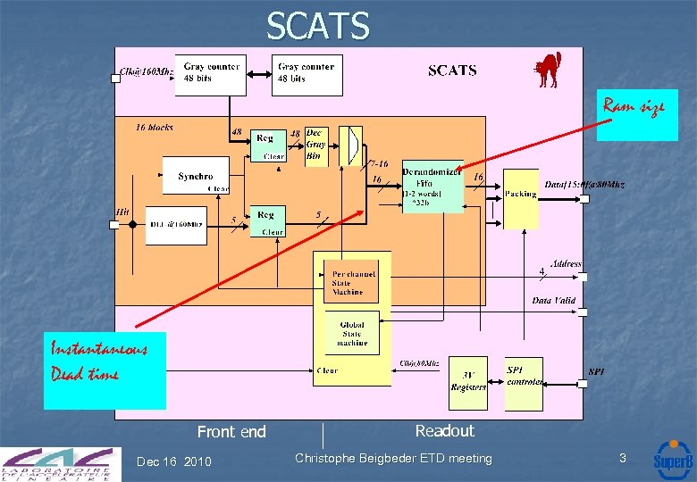 SCATS Ram size Instantaneous Dead time Front end Dec 16 2010 Readout Christophe Beigbeder ETD meeting 3
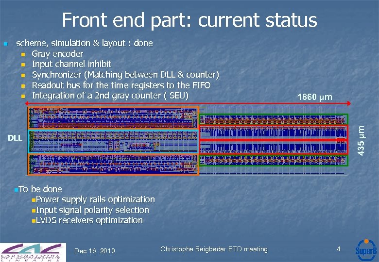 Front end part: current status scheme, simulation & layout : done n Gray encoder n Input channel inhibit n Synchronizer (Matching between DLL & counter) n Readout bus for the time registers to the FIFO n Integration of a 2 nd gray counter ( SEU) 1860 µm 435 µm n DLL n. To be done n. Power supply rails optimization n. Input signal polarity selection n. LVDS receivers optimization Dec 16 2010 Christophe Beigbeder ETD meeting 4
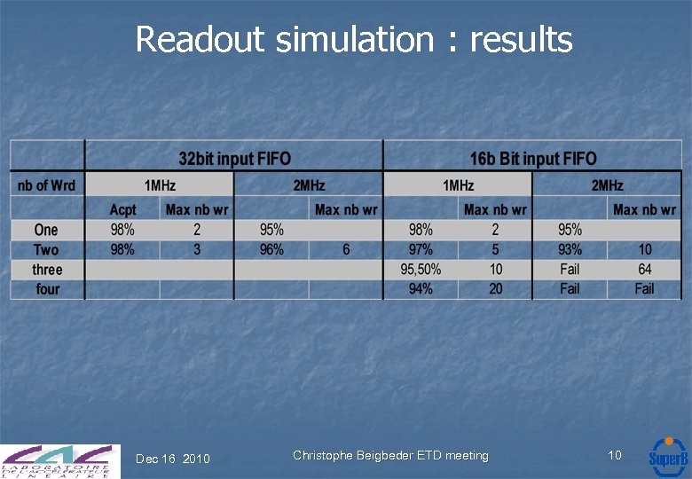
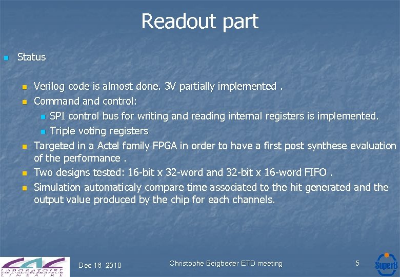 Readout part n Status n n n Verilog code is almost done. 3 V partially implemented. Command control: n SPI control bus for writing and reading internal registers is implemented. n Triple voting registers Targeted in a Actel family FPGA in order to have a first post synthese evaluation of the performance. Two designs tested: 16 -bit x 32 -word and 32 -bit x 16 -word FIFO. Simulation automaticaly compare time associated to the hit generated and the output value produced by the chip for each channels. Dec 16 2010 Christophe Beigbeder ETD meeting 5
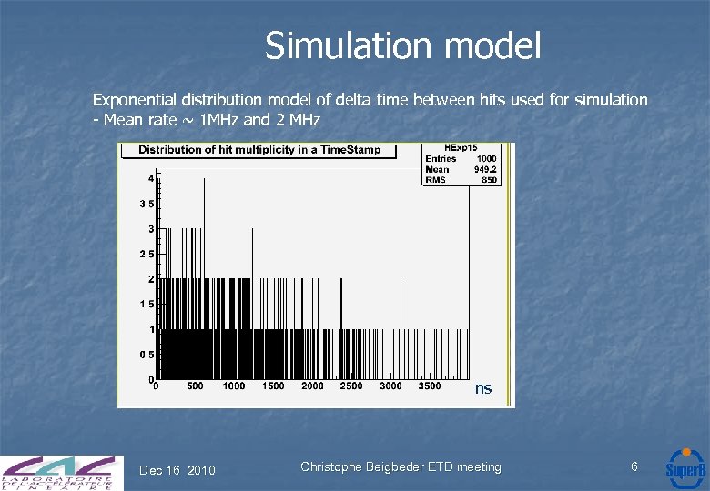 Simulation model Exponential distribution model of delta time between hits used for simulation - Mean rate ~ 1 MHz and 2 MHz ns Dec 16 2010 Christophe Beigbeder ETD meeting 6
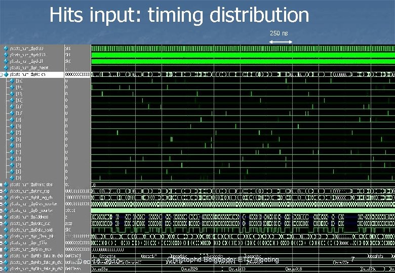 Hits input: timing distribution 250 ns Dec 16 2010 Christophe Beigbeder ETD meeting 7
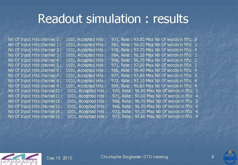 Readout simulation : results Nb Nb Nb Nb Of Of Of Of Input Input Input Input Hits Hits Hits Hits channel 0 : channel 1 : channel 2 : channel 3 : channel 4 : channel 5 : channel 6 : channel 7 : channel 8 : channel 9 : channel 10 : channel 11 : channel 12 : channel 13 : channel 14 : channel 15 : 1001, Accepted Hits : 1001, Accepted Hits : 1001, Accepted Hits : 1001, Accepted Hits : Dec 16 2010 971, Rate : 97. 00 Max Nb Of words in fifo: 961, Rate : 96. 00 Max Nb Of words in fifo: 978, Rate : 97. 70 Max Nb Of words in fifo: 964, Rate : 96. 30 Max Nb Of words in fifo: 968, Rate : 96. 70 Max Nb Of words in fifo: 971, Rate : 97. 00 Max Nb Of words in fifo: 965, Rate : 96. 40 Max Nb Of words in fifo: 977, Rate : 97. 60 Max Nb Of words in fifo: 972, Rate : 97. 10 Max Nb Of words in fifo: 969, Rate : 96. 80 Max Nb Of words in fifo: 970, Rate : 96. 90 Max Nb Of words in fifo: 971, Rate : 97. 00 Max Nb Of words in fifo: 968, Rate : 96. 70 Max Nb Of words in fifo: 972, Rate : 97. 10 Max Nb Of words in fifo: 977, Rate : 97. 60 Max Nb Of words in fifo: Christophe Beigbeder ETD meeting 2 3 4 3 3 3 4 5 4 4 4 8
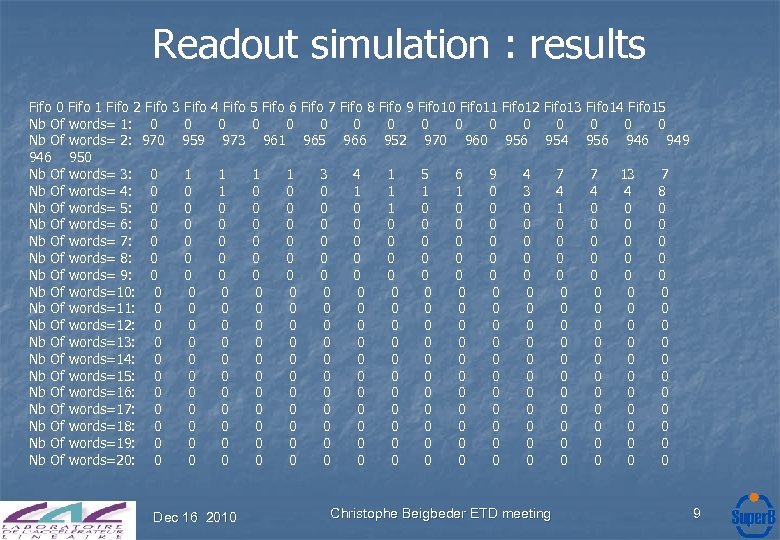 Readout simulation : results Fifo 0 Fifo 1 Fifo 2 Fifo 3 Fifo Nb Of words= 1: 0 0 Nb Of words= 2: 970 959 946 950 Nb Of words= 3: 0 1 Nb Of words= 4: 0 0 Nb Of words= 5: 0 0 Nb Of words= 6: 0 0 Nb Of words= 7: 0 0 Nb Of words= 8: 0 0 Nb Of words= 9: 0 0 Nb Of words=10: 0 0 Nb Of words=11: 0 0 Nb Of words=12: 0 0 Nb Of words=13: 0 0 Nb Of words=14: 0 0 Nb Of words=15: 0 0 Nb Of words=16: 0 0 Nb Of words=17: 0 0 Nb Of words=18: 0 0 Nb Of words=19: 0 0 Nb Of words=20: 0 0 4 Fifo 5 Fifo 6 Fifo 7 Fifo 8 Fifo 9 Fifo 10 Fifo 11 Fifo 12 Fifo 13 Fifo 14 Fifo 15 0 0 0 0 973 961 965 966 952 970 960 956 954 956 949 1 1 0 0 0 0 Dec 16 2010 1 0 0 0 0 0 0 0 0 0 3 0 0 0 0 0 4 1 0 0 0 0 1 1 1 0 0 0 0 5 1 0 0 0 0 6 1 0 0 0 0 9 0 0 0 0 0 4 3 0 0 0 0 Christophe Beigbeder ETD meeting 7 4 1 0 0 0 0 7 4 0 0 0 0 13 4 0 0 0 0 7 8 0 0 0 0 9
 Readout simulation : results Dec 16 2010 Christophe Beigbeder ETD meeting 10
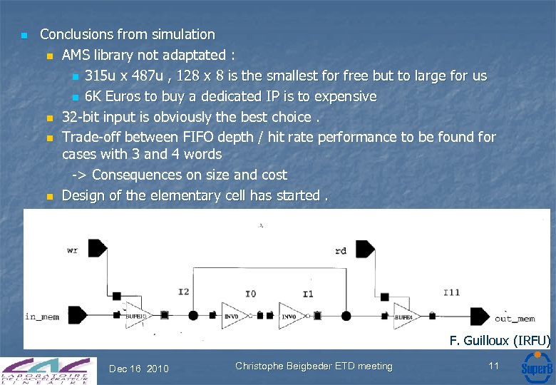 n Conclusions from simulation n AMS library not adaptated : n 315 u x 487 u , 128 x 8 is the smallest for free but to large for us n 6 K Euros to buy a dedicated IP is to expensive n 32 -bit input is obviously the best choice. n Trade-off between FIFO depth / hit rate performance to be found for cases with 3 and 4 words -> Consequences on size and cost n Design of the elementary cell has started. F. Guilloux (IRFU) Dec 16 2010 Christophe Beigbeder ETD meeting 11
 Front end chip - No relevant progress on PIF has been done since last meeting. - From the simulation of the SCATS, the specs for the output design architecture and the synchronisation of the PIF can be studied more precisely : - FIFO in each channel ( complexity ) - Output mux or 16 outputs ( pinout issue ) - Synchronisation between TDC and PIF ( handshake or adjustable timing setup) - ADC issue. Dec 16 2010 Christophe Beigbeder ETD meeting 12
 Next Steps n n n PIF: ongoing design – 1 rst prototype: end of 2011 SCATS : Submission: mai of 2011 – 1 rst prototype in August 2011. Mother board to be developped. PM backplane for the FBLOCK to be developed. Contact has been taken with colleagues from Bari to rapidly develop a prototype of a barrel front end electronics Dec 16 2010 Christophe Beigbeder ETD meeting 13
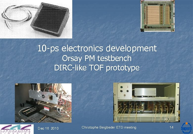 10 -ps electronics development Orsay PM testbench DIRC-like TOF prototype Dec 16 2010 Christophe Beigbeder ETD meeting 14
 Introduction n For the two-bar TOF test at SLAC, we decided to build a synchronous sixteen channel acquisition system based on 8 two-channel Wave. Catcher V 5 boards. n Technical challenge: to keep the 10 ps precision at the crate level – The system has to work with a common synchronous clock § – It is self-triggered but it also has to be synchronized with the rest of the CRT § – There we take benefit of the external clock input of the Wave. Catcher V 5 Rate of cosmics is low thus computer time tagging of events is adequate (if all computers are finely synchronized) Like the Wave. Catcher, data acquisition is based on 480 Mbits/s USB. Dec 16 2010 Christophe Beigbeder ETD meeting 15
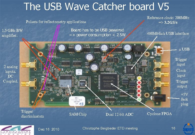 The USB Wave Catcher board V 5 Reference clock: 200 MHz => 3. 2 GS/s Pulsers for reflectometry applications Board has to be USB powered => power consumption < 2. 5 W 1. 5 GHz BW amplifier. 480 Mbits/s USB interface µ USB Trigger input 2 analog inputs. DC Coupled. Clock input Trigger output +5 V Jack plug Trigger discriminators Dec 16 2010 SAM Chip Dual 12 -bit ADC Christophe Beigbeder ETD meeting Cyclone FPGA 16
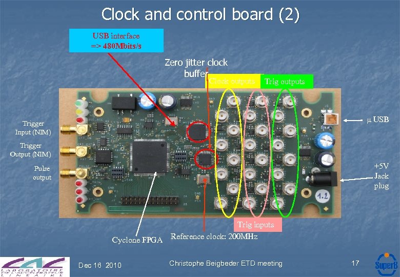 Clock and control board (2) USB interface => 480 Mbits/s Zero jitter clock buffer Clock outputs Trig outputs µ USB Trigger Input (NIM) Trigger Output (NIM) +5 V Jack plug Pulse output Trig inputs Cyclone FPGA Reference clock: 200 MHz Dec 16 2010 Christophe Beigbeder ETD meeting 17
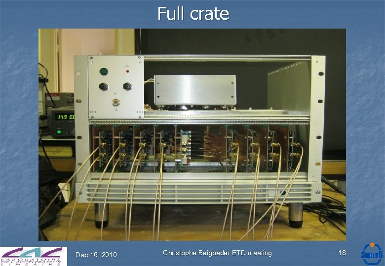 Full crate Dec 16 2010 Christophe Beigbeder ETD meeting 18
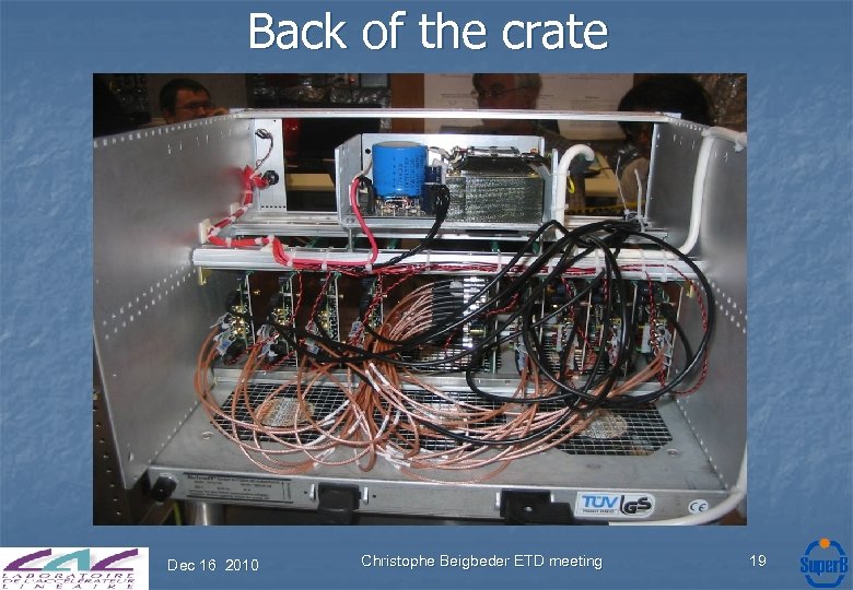 Back of the crate Dec 16 2010 Christophe Beigbeder ETD meeting 19
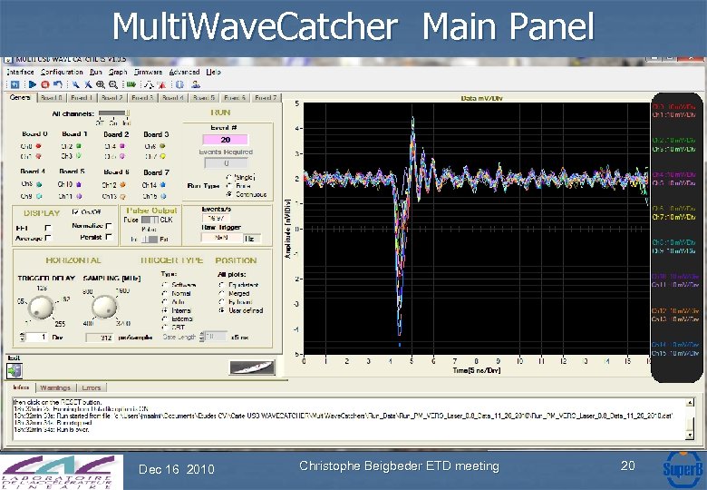 Multi. Wave. Catcher Main Panel Dec 16 2010 Christophe Beigbeder ETD meeting 20
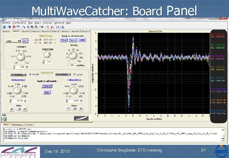 Multi. Wave. Catcher: Board Panel Dec 16 2010 Christophe Beigbeder ETD meeting 21
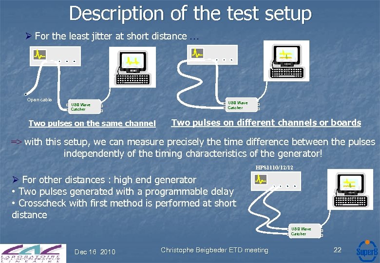 Description of the test setup Ø For the least jitter at short distance … Open cable USB Wave Catcher Two pulses on the same channel USB Wave Catcher Two pulses on different channels or boards => with this setup, we can measure precisely the time difference between the pulses independently of the timing characteristics of the generator! HP 81110/12/12 Ø For other distances : high end generator • Two pulses generated with a programmable delay • Crosscheck with first method is performed at short distance USB Wave Catcher Dec 16 2010 Christophe Beigbeder ETD meeting 22
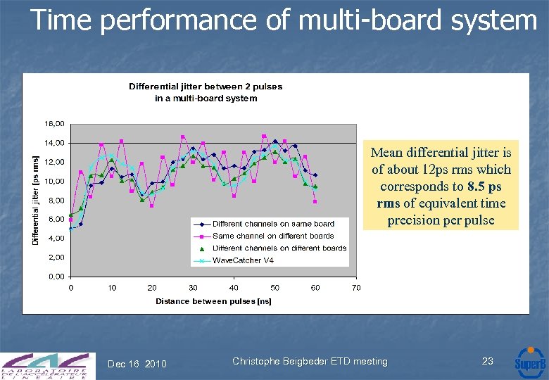 Time performance of multi-board system Mean differential jitter is of about 12 ps rms which corresponds to 8. 5 ps rms of equivalent time precision per pulse Dec 16 2010 Christophe Beigbeder ETD meeting 23
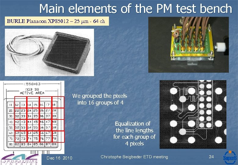 Main elements of the PM test bench BURLE Planacon XP 85012 – 25 µm - 64 ch We grouped the pixels into 16 groups of 4 Equalization of the line lengths for each group of 4 pixels Dec 16 2010 Christophe Beigbeder ETD meeting 24
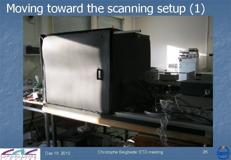 Moving toward the scanning setup (1) Dec 16 2010 Christophe Beigbeder ETD meeting 25
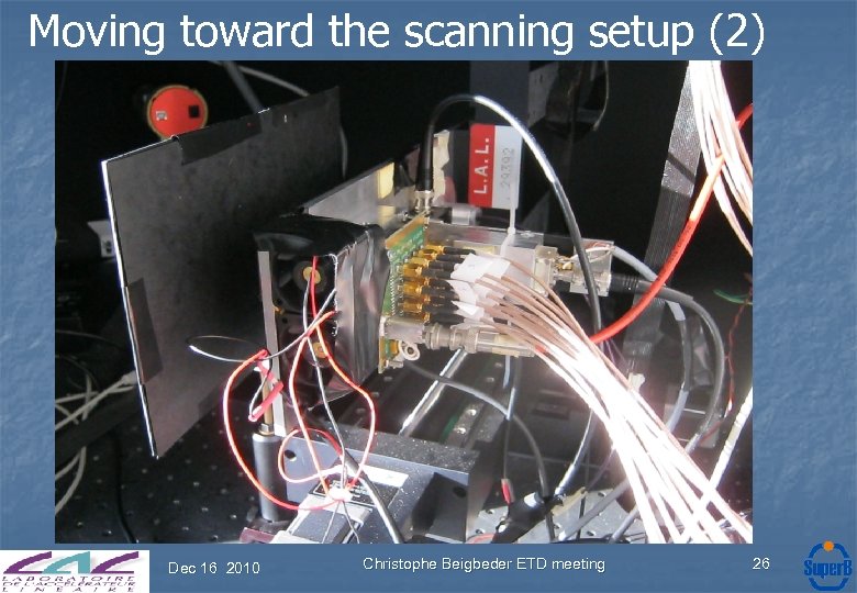 Moving toward the scanning setup (2) Dec 16 2010 Christophe Beigbeder ETD meeting 26
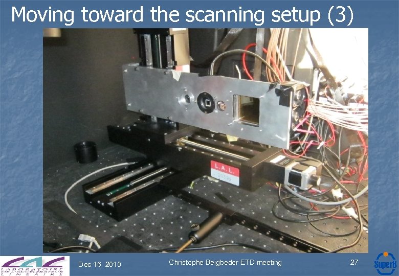 Moving toward the scanning setup (3) Dec 16 2010 Christophe Beigbeder ETD meeting 27
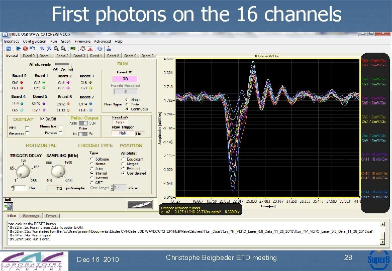 First photons on the 16 channels Dec 16 2010 Christophe Beigbeder ETD meeting 28
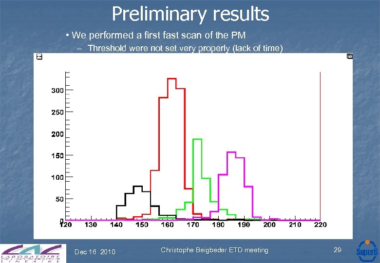 Preliminary results • We performed a first fast scan of the PM – Threshold were not set very properly (lack of time) – Example of an horizontal crossing efficiency plot Plot de Leonid mm Dec 16 2010 Christophe Beigbeder ETD meeting 29
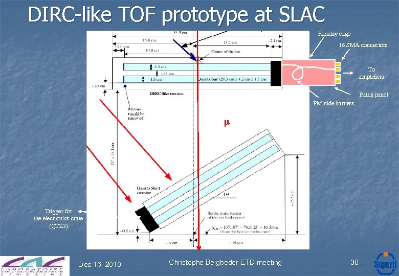 DIRC-like TOF prototype at SLAC Faraday cage 16 SMA connectors To amplifiers Patch panel PM-side harness µ MCPPMT Trigger for the electronics crate (QTZ 3) Dec 16 2010 Christophe Beigbeder ETD meeting 30
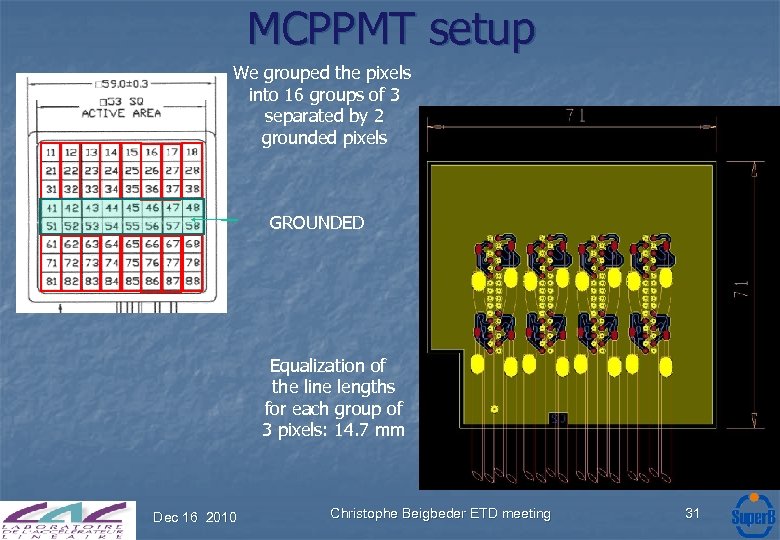 MCPPMT setup We grouped the pixels into 16 groups of 3 separated by 2 grounded pixels GROUNDED Equalization of the line lengths for each group of 3 pixels: 14. 7 mm Dec 16 2010 Christophe Beigbeder ETD meeting 31
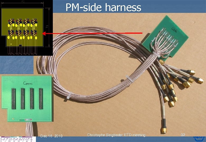 PM-side harness Dec 16 2010 Christophe Beigbeder ETD meeting 32
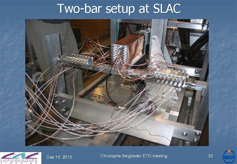 Two-bar setup at SLAC Dec 16 2010 Christophe Beigbeder ETD meeting 33
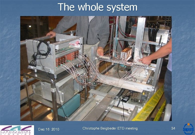 The whole system Dec 16 2010 Christophe Beigbeder ETD meeting 34
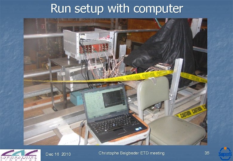 Run setup with computer Dec 16 2010 Christophe Beigbeder ETD meeting 35
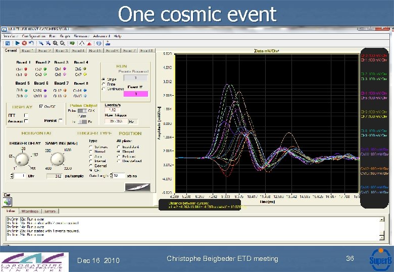 One cosmic event • Recycled 6 U crate • Naked Wave. Catchers mounted on 3 U carrier boards Dec 16 2010 Christophe Beigbeder ETD meeting 36
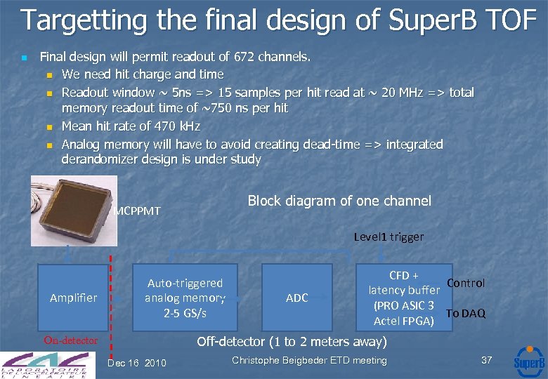 Targetting the final design of Super. B TOF n Final design will permit readout of 672 channels. n We need hit charge and time n Readout window ~ 5 ns => 15 samples per hit read at ~ 20 MHz => total memory readout time of ~750 ns per hit n Mean hit rate of 470 k. Hz n Analog memory will have to avoid creating dead-time => integrated derandomizer design is under study Block diagram of one channel MCPPMT Level 1 trigger Amplifier Auto-triggered analog memory 2 -5 GS/s ADC CFD + Control latency buffer (PRO ASIC 3 To DAQ Actel FPGA) Off-detector (1 to 2 meters away) On-detector Dec 16 2010 Christophe Beigbeder ETD meeting 37
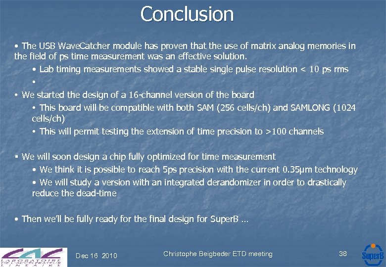 Conclusion • The USB Wave. Catcher module has proven that the use of matrix analog memories in the field of ps time measurement was an effective solution. • Lab timing measurements showed a stable single pulse resolution < 10 ps rms • • We started the design of a 16 -channel version of the board • This board will be compatible with both SAM (256 cells/ch) and SAMLONG (1024 cells/ch) • This will permit testing the extension of time precision to >100 channels § We will soon design a chip fully optimized for time measurement • We think it is possible to reach 5 ps precision with the current 0. 35µm technology • We will study a version with an integrated derandomizer in order to drastically reduce the dead-time • Then we’ll be fully ready for the final design for Super. B … Dec 16 2010 Christophe Beigbeder ETD meeting 38


