Physics of Semiconductor Devices Lecture 7. I-V

lecture_7.pptx
- Размер: 717.7 Кб
- Автор:
- Количество слайдов: 15
Описание презентации Physics of Semiconductor Devices Lecture 7. I-V по слайдам
 Physics of Semiconductor Devices Lecture 7. I-V Characteristics of Ideal P-N Junction A. V. Sogoyan
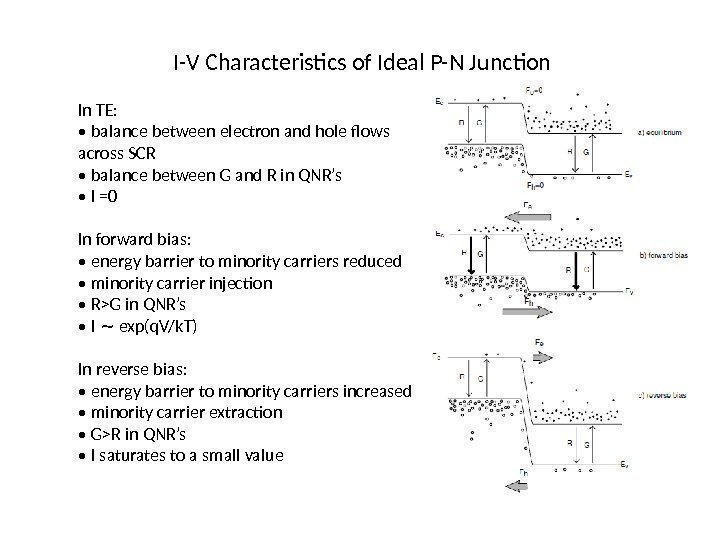
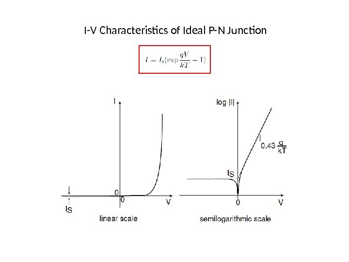
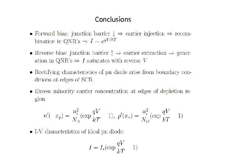
 I-V Characteristics of Ideal P-N Junction In TE: • balance between electron and hole flows across SCR • balance between G and R in QNR’s • I =0 In forward bias: • energy barrier to minority carriers reduced • minority carrier injection • R>G in QNR’s • I exp(q. V/k. T)∼ In reverse bias: • energy barrier to minority carriers increased • minority carrier extraction • G>R in QNR’s • I saturates to a small value
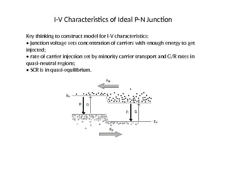
 I-V Characteristics of Ideal P-N Junction Key thinking to construct model for I-V characteristics: • junction voltage sets concentration of carriers with enough energy to get injected; • rate of carrier injection set by minority carrier transport and G/R rates in quasi-neutral regions; • SCR is in quasi-equilibrium.
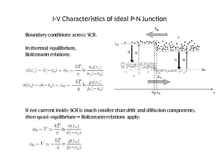
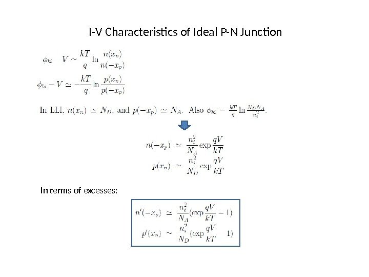
 I-V Characteristics of Ideal P-N Junction Boundary conditions across SCR. In thermal equilibrium, Boltzmann relations: If net current inside SCR is much smaller than drift and diffusion components, then quasi-equilibrium Boltzmann relations apply: ⇒
 I-V Characteristics of Ideal P-N Junction In terms of excesses:
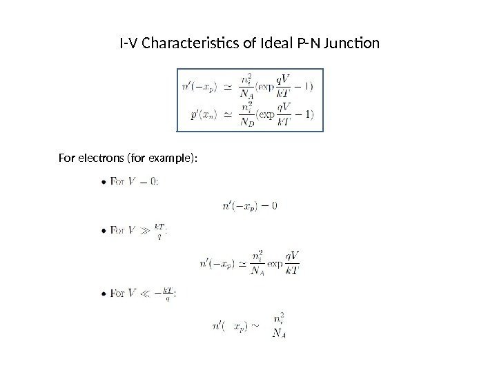
 I-V Characteristics of Ideal P-N Junction For electrons (for example):
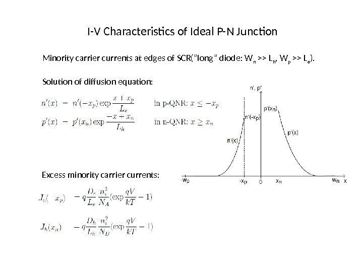
 I-V Characteristics of Ideal P-N Junction Minority carrier currents at edges of SCR(”long” diode: W n >> L h , W p >> L e ). Solution of diffusion equation: Excess minority carrier currents:
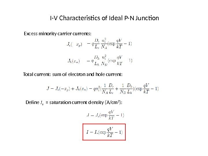
 I-V Characteristics of Ideal P-N Junction Excess minority carrier currents: Total current: sum of electron and hole current: Define J s ≡ saturation current density (A/cm 2 ):
 I-V Characteristics of Ideal P-N Junction
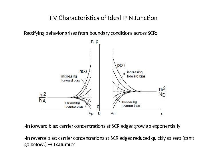
 I-V Characteristics of Ideal P-N Junction Rectifying behavior arises from boundary conditions across SCR: -In forward bias: carrier concentrations at SCR edges grow up exponentially -In reverse bias: carrier concentrations at SCR edges reduced quickly to zero (can’t go below!) → I saturates
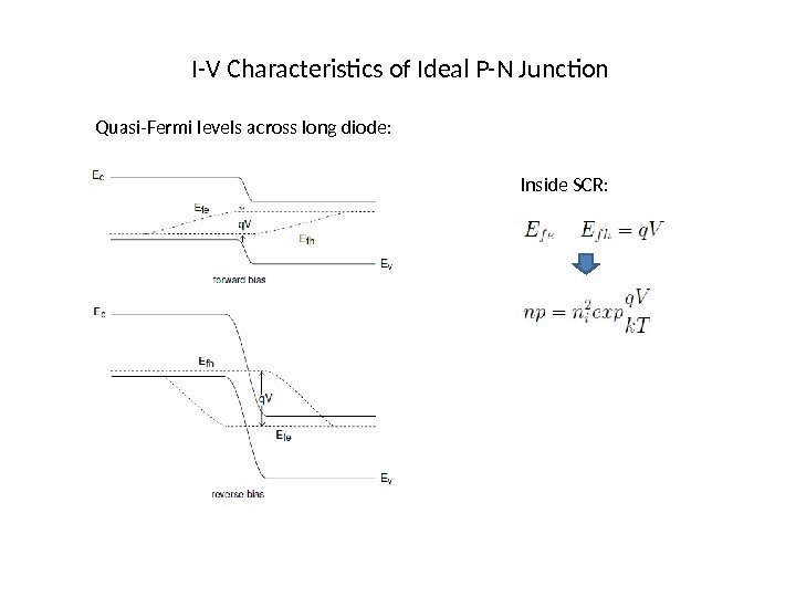
 I-V Characteristics of Ideal P-N Junction Quasi-Fermi levels across long diode: Inside SCR:
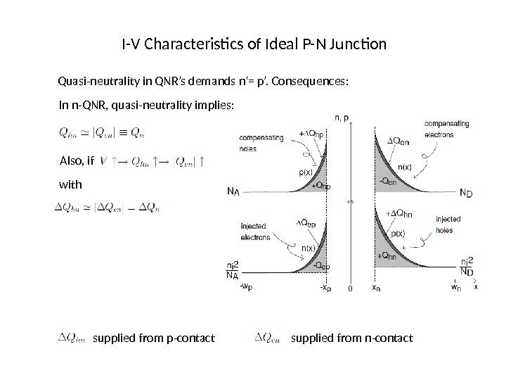
 I-V Characteristics of Ideal P-N Junction Quasi-neutrality in QNR’s demands n‘= p’. Consequences: In n-QNR, quasi-neutrality implies: Also, if with supplied from p-contact supplied from n-contact
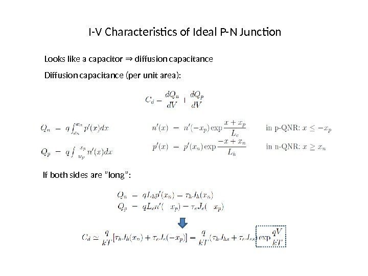
 I-V Characteristics of Ideal P-N Junction Looks like a capacitor diffusion capacitance⇒ Diffusion capacitance (per unit area): If both sides are ”long”:
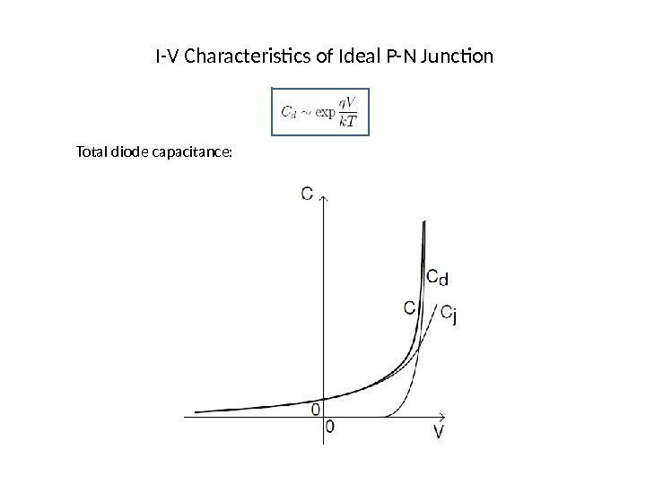
 I-V Characteristics of Ideal P-N Junction Total diode capacitance:
 Conclusions

