ab7cdb727dbae6e91c4338cdca6f5d43.ppt
- Количество слайдов: 30
 Physical Vapor Deposition
 PVD n Physical methods produce the atoms that deposit on the substrate – Evaporation – Sputtering n Sometimes called vacuum deposition because the process is usually done in an evacuated chamber § PVD is used for metals. § Dielectrics can be deposited using specialized equipment
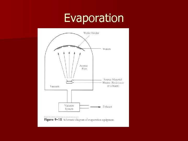
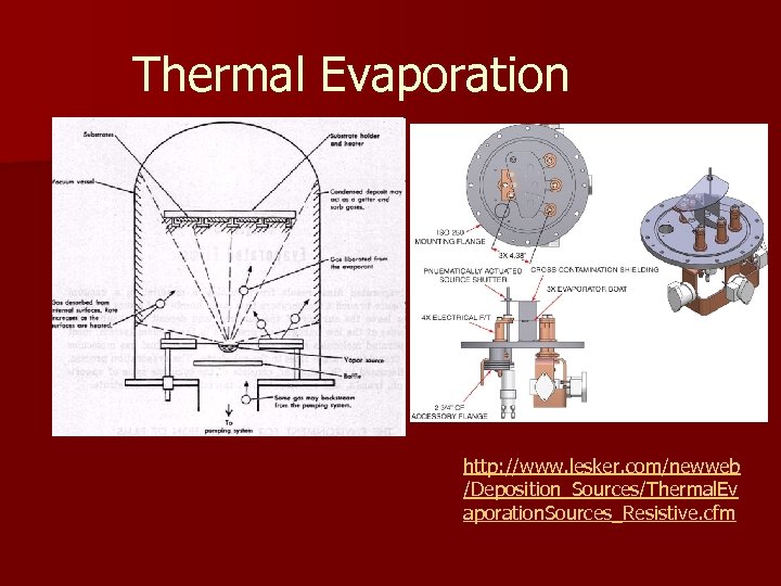
 Evaporation Rely on thermal energy supplied to the crucible or boat to evaporate atoms n Evaporated atoms travel through the evacuated space between the source and the sample and stick to the sample n – Few, if any, chemical reactions occur due to low pressure – Can force a reaction by flowing a gas near the crucible n Surface reactions usually occur very rapidly and there is very little rearrangement of the surface atoms after sticking – Thickness uniformity and shadowing by surface topography, and step coverage are issues
 Evaporation
 http: //www. ee. byu. edu/cleanroom/metal. parts/vaporpressure. jpg
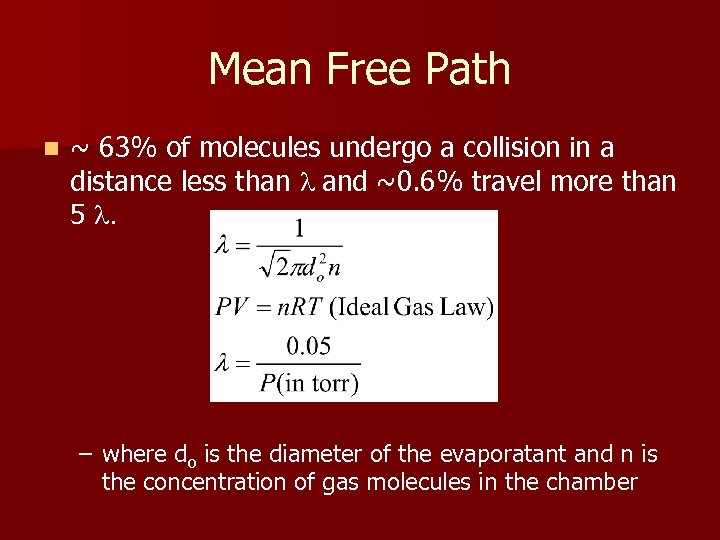 Mean Free Path n ~ 63% of molecules undergo a collision in a distance less than l and ~0. 6% travel more than 5 l. – where do is the diameter of the evaporatant and n is the concentration of gas molecules in the chamber
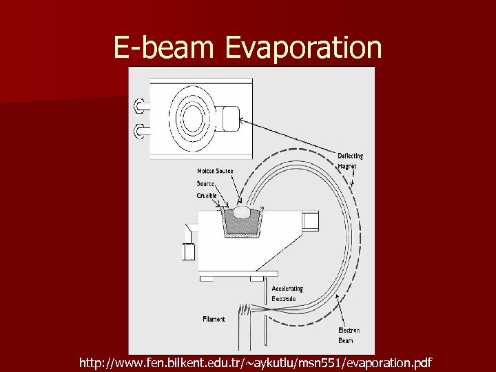
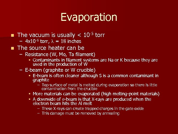 Evaporation n The vacuum is usually < 10 -5 torr n The source heater can be – 4 x 10 -6 torr, l = 18 inches – Resistance (W, Mo, Ta filament) § Contaminants in filament systems are Na or K because they are used in the production of W – E-beam (graphite or W crucible) § E-beam is often cleaner although S is a common contaminant in graphite – Top surface of metal is melted during evaporation so there is little contamination from the crucible § More materials can be evaporated (high melting-point materials) § A downside of e-beam is that X-rays are produced when the electron beam hits the Al melt – These X-rays can create trapped charges in the gate oxide – This damage must be removed by annealing
 Thermal Evaporation http: //www. lesker. com/newweb /Deposition_Sources/Thermal. Ev aporation. Sources_Resistive. cfm
 E-beam Evaporation http: //www. fen. bilkent. edu. tr/~aykutlu/msn 551/evaporation. pdf
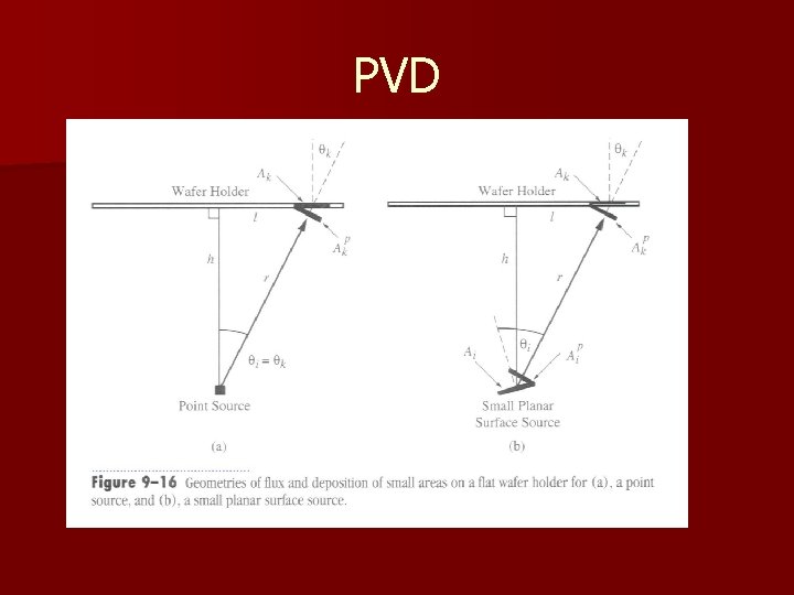
 PVD n At sufficiently low pressure and reasonable distances between source and wafer, evaporant travel in straight line to the wafer – Step coverage is close to zero – If the source is small, we can treat it as a point source – If the source emission is isotropic, it is easy to compute the distribution of atoms at the surface of the wafer
 PVD
PVD
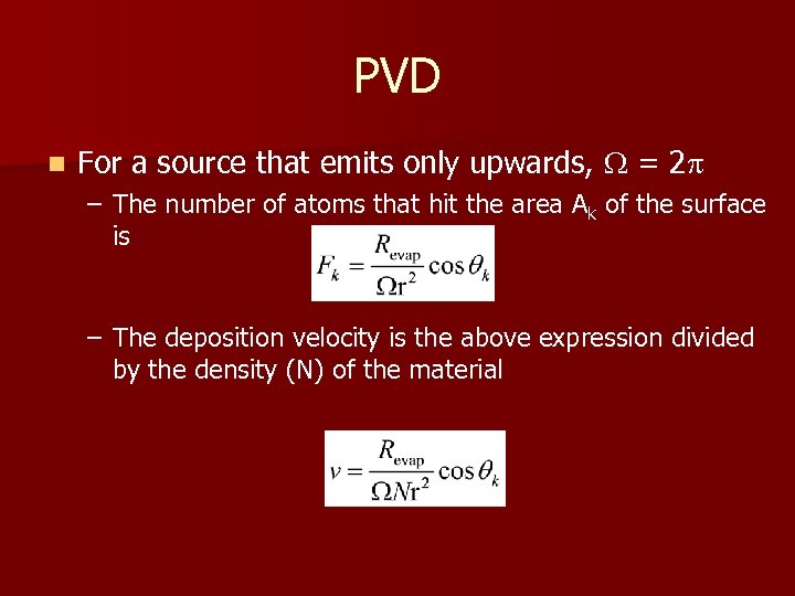 PVD n For a source that emits only upwards, = 2 – The number of atoms that hit the area Ak of the surface is – The deposition velocity is the above expression divided by the density (N) of the material
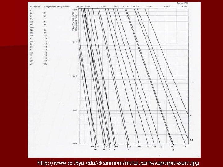
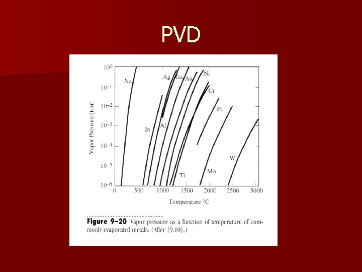
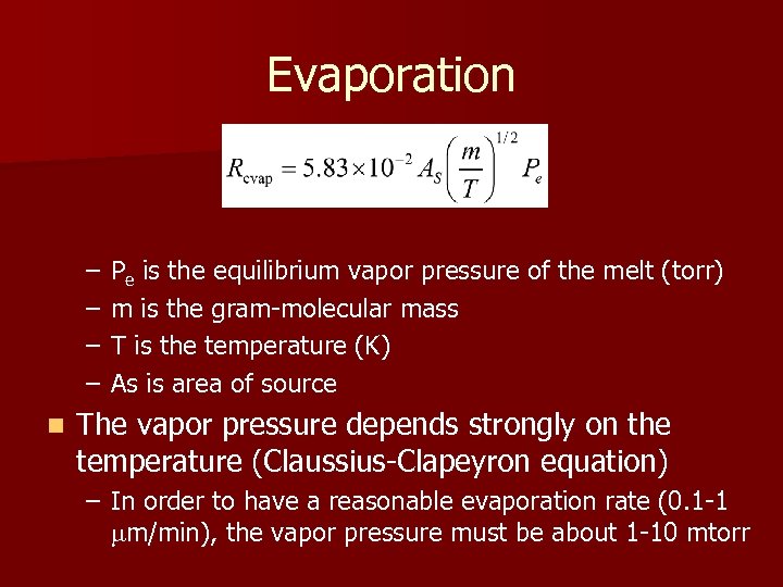 Evaporation – – n Pe is the equilibrium vapor pressure of the melt (torr) m is the gram-molecular mass T is the temperature (K) As is area of source The vapor pressure depends strongly on the temperature (Claussius-Clapeyron equation) – In order to have a reasonable evaporation rate (0. 1 -1 m/min), the vapor pressure must be about 1 -10 mtorr
 PVD
PVD
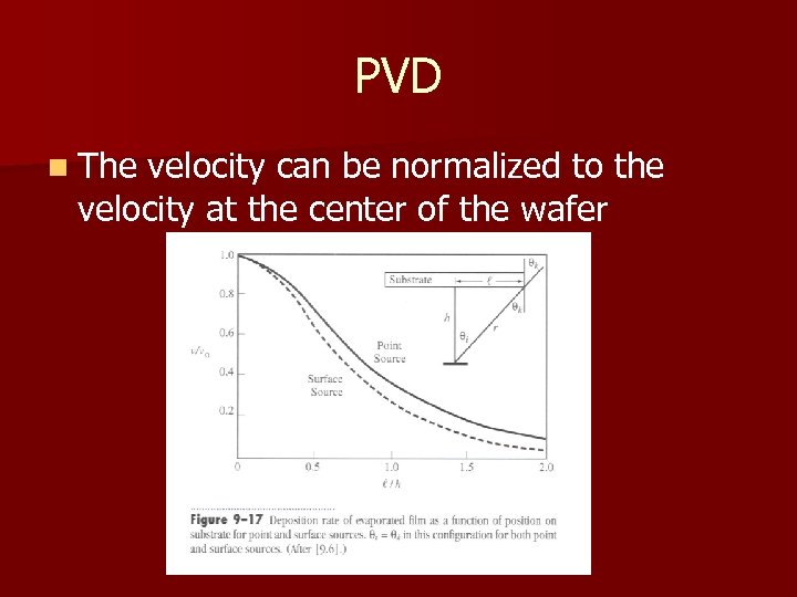 PVD n The velocity can be normalized to the velocity at the center of the wafer
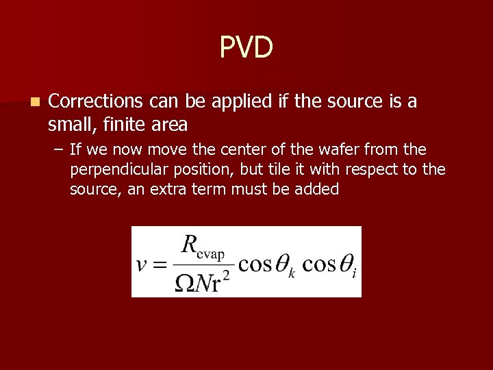 PVD n Corrections can be applied if the source is a small, finite area – If we now move the center of the wafer from the perpendicular position, but tile it with respect to the source, an extra term must be added
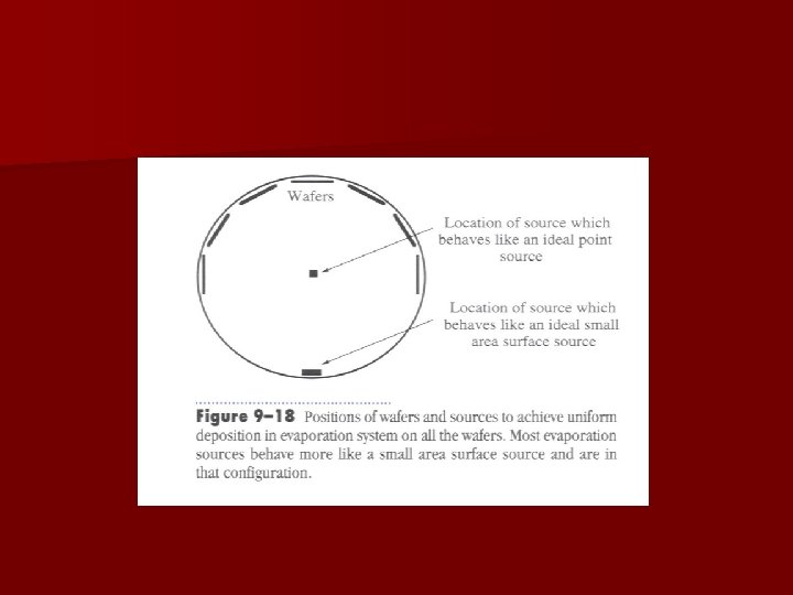
 Planetaries n Wafer holders that rotate wafer position during deposition to increase film thickness uniformity across wafer and from one wafer to another. – Wobbling wafer holders increase step coverage
 PVD n Nonuniformity of evaporatant can occur when angular emission of evaporant is narrower than the ideal source – Crucible geometry – Melt depth to melt area ratio – Density of gas atoms over the surface of the melt
 Evaporation n Evaporating alloys is difficult Because of the differing vapor pressures. – Composition of the deposited material may very different from that of the target material n The problem can be overcome by – Using multiple e-beams on multiple sources § This technique causes difficulties in sample uniformity because of the spacing of the sources – Evaporating source to completion (until no material is left) § Dangerous to do in e-beam system
 Evaporation n Compounds are also hard to evaporate because the molecular species may be different from the compound composition – Energy provided may be used to dissociate compound. – When evaporating Si. O 2, Si. O is deposited. Evaporation in a reactive environment (flowing O 2 gas near crucible during deposition) helps reconstitute oxide.
 Evaporation n Advantages – Little damage to the wafer – Deposited films are usually very pure – Limited step coverage n Disadvantages – Materials with low vapor pressures ae very difficult to evaporated § Refractory metals § High temperature dielectrics – No in situ precleaning – Limited step coverage – Film adhesion can be problematic
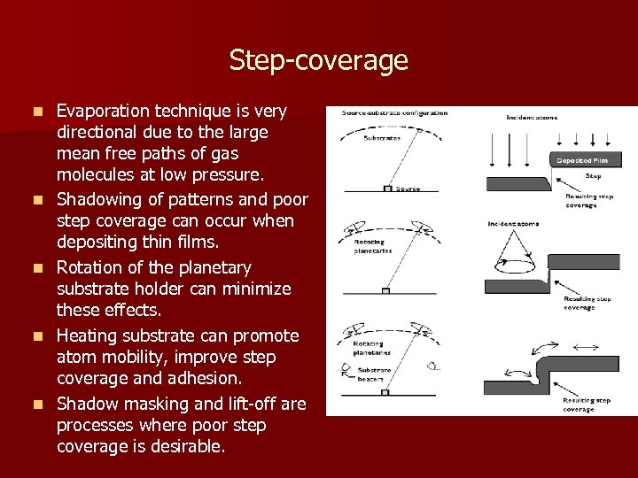 Step-coverage n n n Evaporation technique is very directional due to the large mean free paths of gas molecules at low pressure. Shadowing of patterns and poor step coverage can occur when depositing thin films. Rotation of the planetary substrate holder can minimize these effects. Heating substrate can promote atom mobility, improve step coverage and adhesion. Shadow masking and lift-off are processes where poor step coverage is desirable.
 Other PVD Techniques n Other deposition techniques include – Sputter deposition (DC, RF, and reactive) – Bias sputtering – Magnetron sputtering – Collimated and ionized sputter deposition – Hot sputter deposition
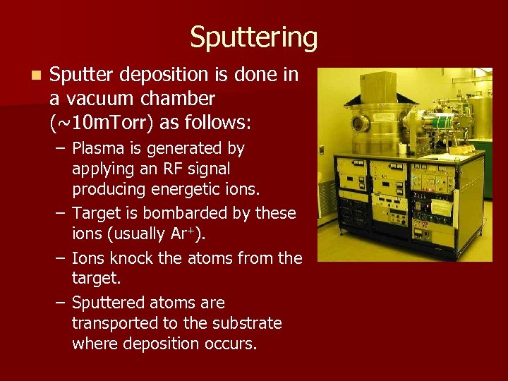 Sputtering n Sputter deposition is done in a vacuum chamber (~10 m. Torr) as follows: – Plasma is generated by applying an RF signal producing energetic ions. – Target is bombarded by these ions (usually Ar+). – Ions knock the atoms from the target. – Sputtered atoms are transported to the substrate where deposition occurs.
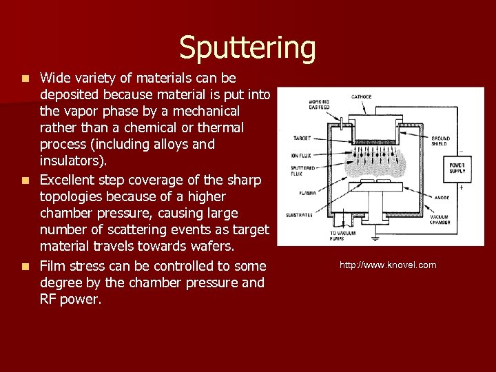 Sputtering Wide variety of materials can be deposited because material is put into the vapor phase by a mechanical rather than a chemical or thermal process (including alloys and insulators). n Excellent step coverage of the sharp topologies because of a higher chamber pressure, causing large number of scattering events as target material travels towards wafers. n Film stress can be controlled to some degree by the chamber pressure and RF power. n http: //www. knovel. com
 Deposition conditions n Temperature: Room to higher n Pressure: 100 mtorr – compromise between increasing number of Ar ions and increasing scattering of Ar ions with neutral Ar atoms n Power – Heating of target material § Low temperature metals can melt from temperature rise caused by energy transfer from Ar ions
 Sputter sources n Magnetron – Magnetic field traps freed electron near target – Move in helical pattern, causing large number of scattering events with Ar gas – creating high density of ionized Ar n Ion beam – Plasma of ions generated away from target and then accelerated toward start by electric field n Reactive sputtering – Gas used in plasma reacts with target material to form compond that is deposited on wafer n Ion-assisted deposition – Wafer is biased so that some Ar ion impact its surface, density the deposited film. May sputter material off of wafer prior to deposition for in-situ cleaning.
 Sputtering n Advantages – Large-size targets, simplifying the deposition of thins with uniform thickness over large wafers – Film thickness is easily controlled by fixing the operating parameters and simply adjusting the deposition time – Control of the alloy composition, step coverage, grain structure is easier obtained through evaporation – Sputter-cleaning of the substrate in vacuum prior to film deposition – Device damage from X-rays generated by electron beam evaporation is avoided. n Disadvantages – High capital expenses are required – Rates of deposition of some materials (such as Si. O 2) are relatively low – Some materials such as organic solids are easily degraded by ionic bombardment – Greater probability to introduce impurities in the substrate because the former operates under a higher pressure
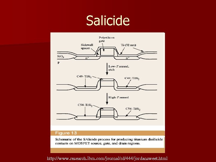 Salicide http: //www. research. ibm. com/journal/rd/444/jordansweet. html


