c540da6d79f8f3a3757254416247cbdc.ppt
- Количество слайдов: 56
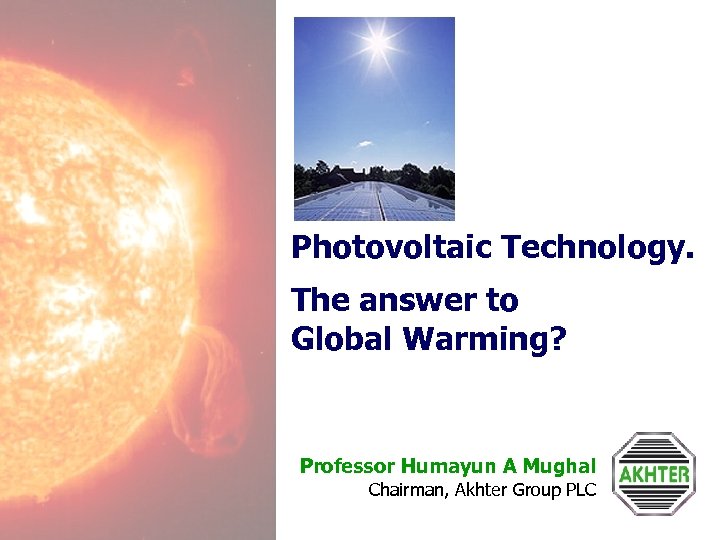
Photovoltaic Technology. The answer to Global Warming? Professor Humayun A Mughal Chairman, Akhter Group PLC
Key Issues Global Warming – a Reality Energy Production – major Contributor Growing Demand for Electricity – no Going back Green Energy – is The Only Option The PHOTOVOLTAIC technology – is the Green Option PV is the ANSWER to our needs - Economic, Environmentally friendly and Renewable
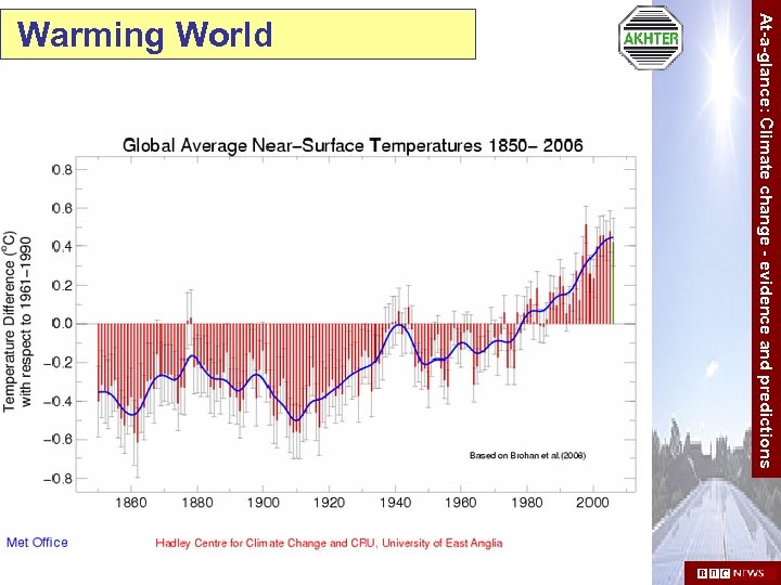
At-a-glance: Climate change - evidence and predictions Warming World
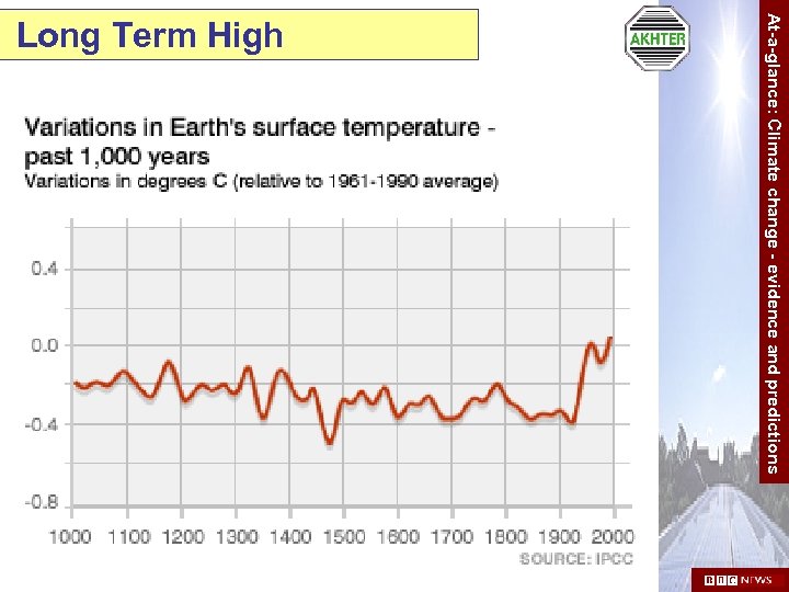
At-a-glance: Climate change - evidence and predictions Long Term High
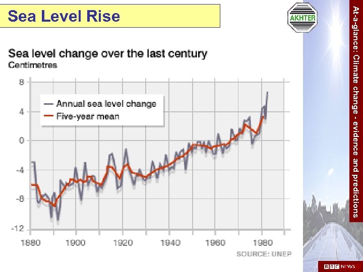
At-a-glance: Climate change - evidence and predictions Sea Level Rise
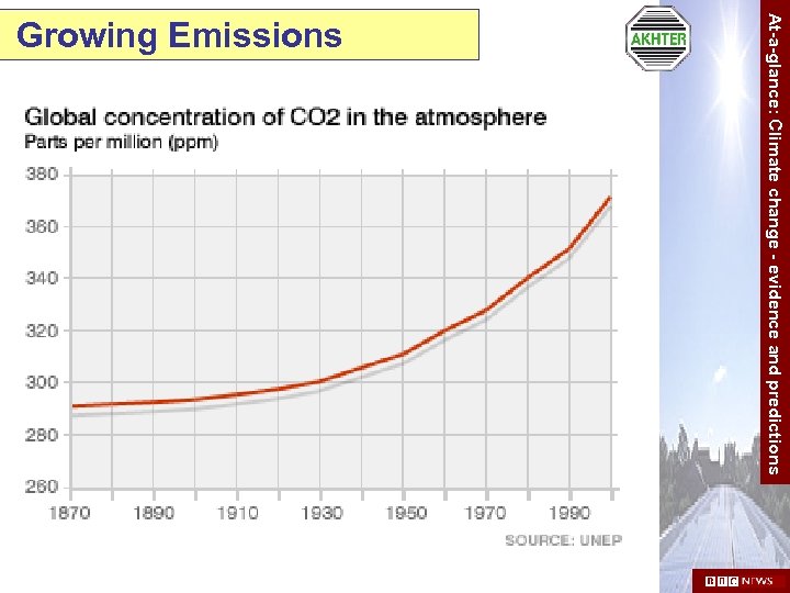
At-a-glance: Climate change - evidence and predictions Growing Emissions
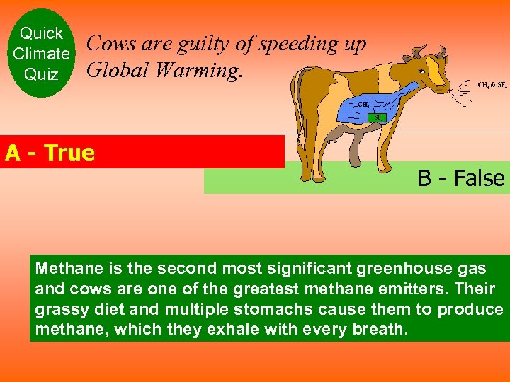
Quick Climate Quiz Cows are guilty of speeding up Global Warming. A - True B - False Methane is the second most significant greenhouse gas and cows are one of the greatest methane emitters. Their grassy diet and multiple stomachs cause them to produce methane, which they exhale with every breath.
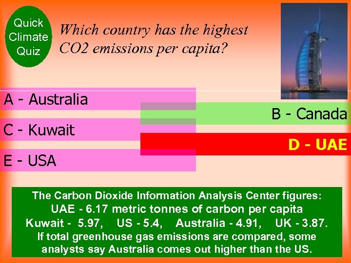
Quick Climate Quiz Which country has the highest CO 2 emissions per capita? A - Australia C - Kuwait E - USA B - Canada D -- UAE D UAE The Carbon Dioxide Information Analysis Center figures: UAE - 6. 17 metric tonnes of carbon per capita Kuwait - 5. 97, US - 5. 4, Australia - 4. 91, UK - 3. 87. If total greenhouse gas emissions are compared, some analysts say Australia comes out higher than the US.
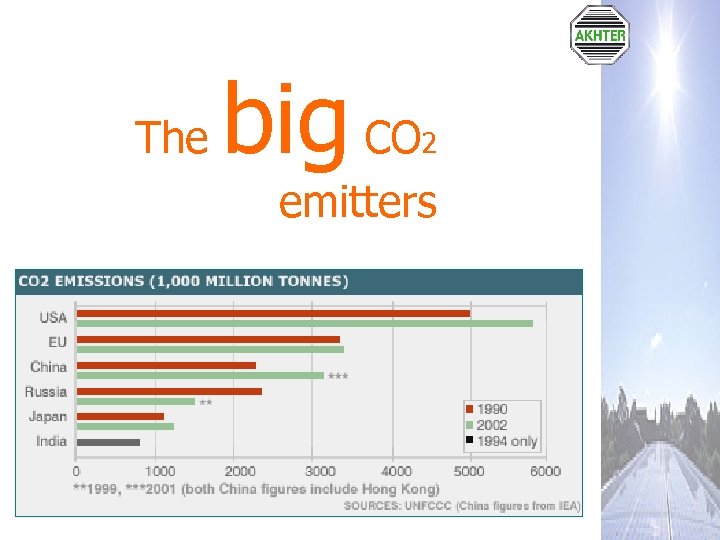
The big CO 2 emitters
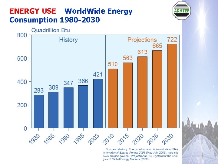
ENERGY USE World. Wide Energy Consumption 1980 -2030
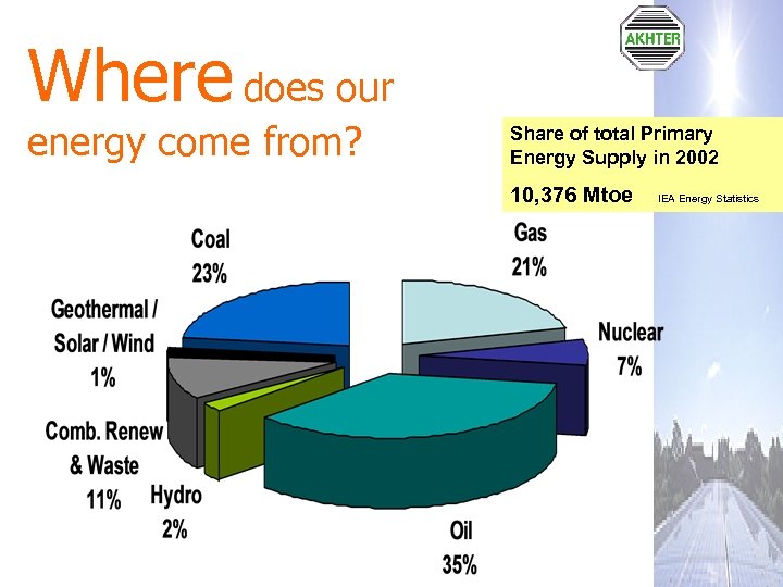
Where does our energy come from? Share of total Primary Energy Supply in 2002 10, 376 Mtoe IEA Energy Statistics
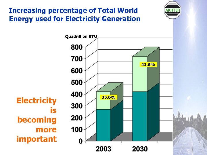
Increasing percentage of Total World Energy used for Electricity Generation Quadrillion BTU 41. 6% Electricity is becoming more important 35. 6%
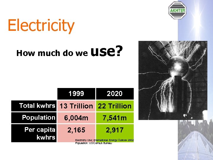
Electricity How much do we 1999 use? 2020 Total kwhrs 13 Trillion 22 Trillion Population Per capita kwhrs 6, 004 m 7, 541 m 2, 165 2, 917 Electricity Use: International Energy Outlook 2002 Population: US Census Bureau
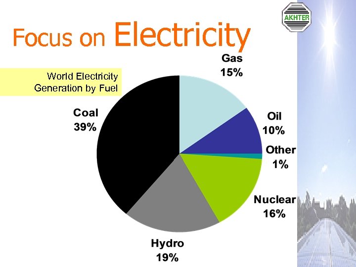
Focus on Electricity World Electricity Generation by Fuel
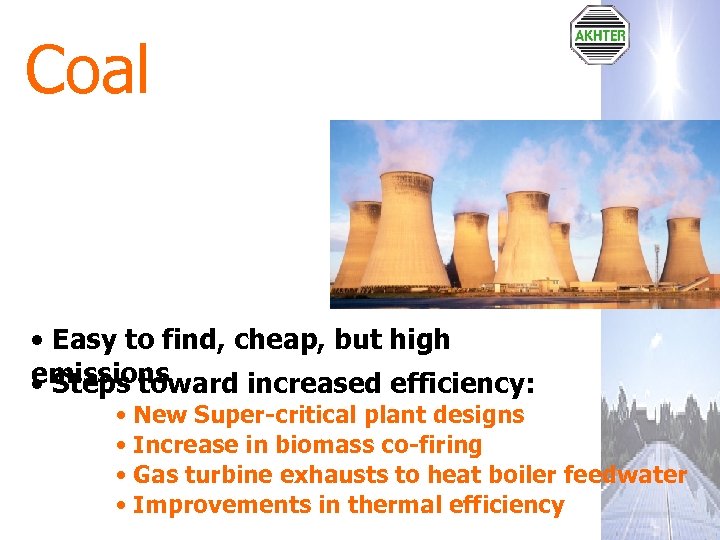
Coal • Easy to find, cheap, but high emissions • Steps toward increased efficiency: • New Super-critical plant designs • Increase in biomass co-firing • Gas turbine exhausts to heat boiler feedwater • Improvements in thermal efficiency
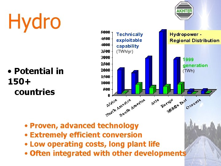
Hydro Technically exploitable capability Hydropower - Regional Distribution (TWh/yr) • Potential in 150+ countries 1999 generation (TWh) • Proven, advanced technology • Extremely efficient conversion • Low operating costs, long plant life • Often integrated with other developments
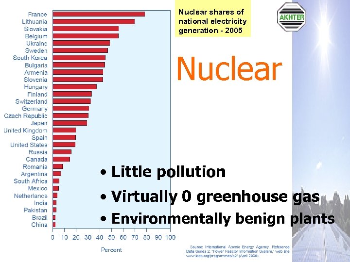
Nuclear shares of national electricity generation - 2005 Nuclear • Little pollution • Virtually 0 greenhouse gas • Environmentally benign plants
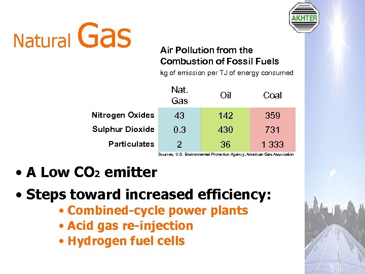
Natural Gas Air Pollution from the Combustion of Fossil Fuels kg of emission per TJ of energy consumed Nat. Gas Oil Coal Nitrogen Oxides 43 142 359 Sulphur Dioxide 0. 3 430 731 2 36 1 333 Particulates Sources: U. S. Environmental Protection Agency; American Gas Association • A Low CO 2 emitter • Steps toward increased efficiency: • Combined-cycle power plants • Acid gas re-injection • Hydrogen fuel cells
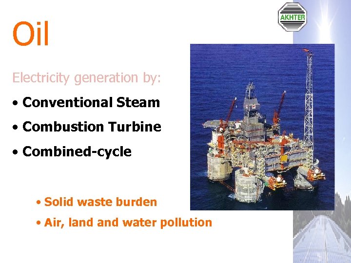
Oil Electricity generation by: • Conventional Steam • Combustion Turbine • Combined-cycle • Solid waste burden • Air, land water pollution
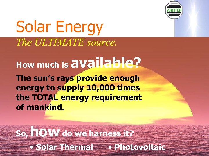
Solar Energy The ULTIMATE source. How much is available? The sun’s rays provide enough energy to supply 10, 000 times the TOTAL energy requirement of mankind. So, how do we harness it? • Solar Thermal • Photovoltaic
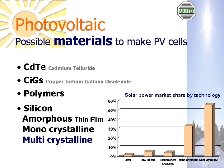
Photovoltaic Possible materials to make PV cells • Cd. Te Cadmium Telluride • Ci. Gs Copper Indium Gallium Diselenide • Polymers Solar power market share by technology • Silicon Amorphous Thin Film Mono crystalline Multi crystalline
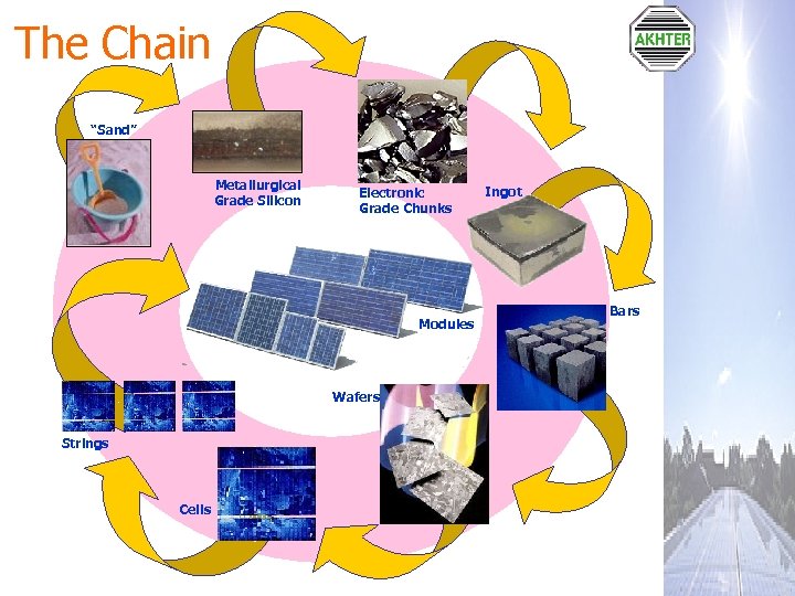
The Chain “Sand” Metallurgical Grade Silicon Electronic Grade Chunks Modules Wafers Strings Cells Ingot Bars
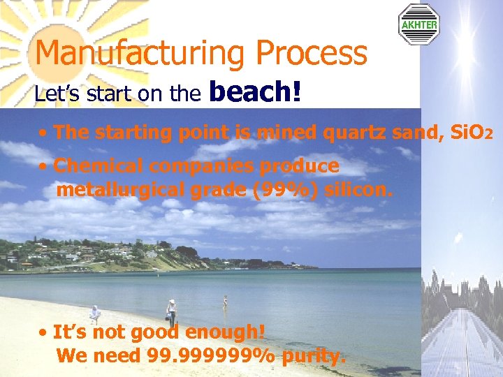
Manufacturing Process Let’s start on the beach! • The starting point is mined quartz sand, Si. O 2 • Chemical companies produce metallurgical grade (99%) silicon. • It’s not good enough! We need 99. 999999% purity.
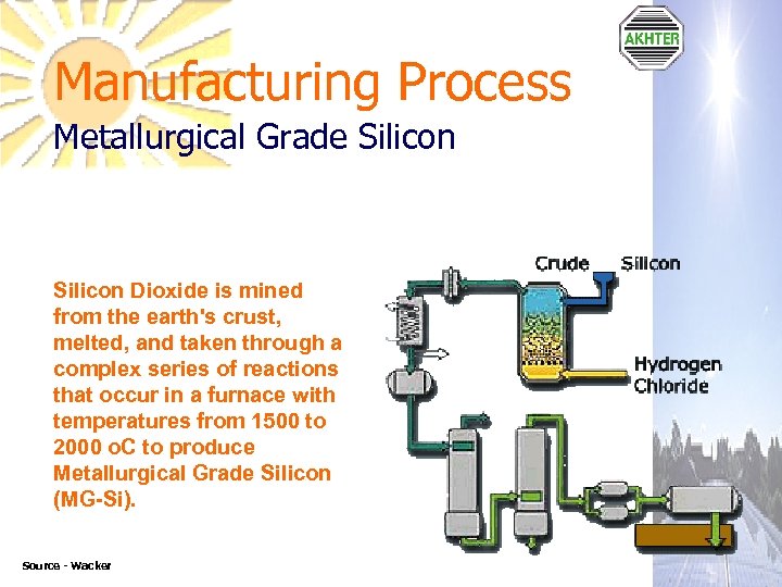
Manufacturing Process Metallurgical Grade Silicon Dioxide is mined from the earth's crust, melted, and taken through a complex series of reactions that occur in a furnace with temperatures from 1500 to 2000 o. C to produce Metallurgical Grade Silicon (MG-Si). Source - Wacker
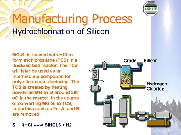
Manufacturing Process Hydrochlorination of Silicon MG-Si is reacted with HCl to form trichlorosilane (TCS) in a fluidized-bed reactor. The TCS will later be used as an intermediate compound for polysilicon manufacturing. The TCS is created by heating powdered MG-Si at around 300 o. C in the reactor. In the course of converting MG-Si to TCS, impurities such as Fe, Al and B are removed. Si + 3 HCl -----> Si. HCL 3 + H 2
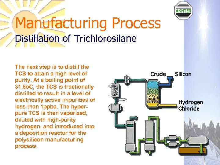
Manufacturing Process Distillation of Trichlorosilane The next step is to distill the TCS to attain a high level of purity. At a boiling point of 31. 8 o. C, the TCS is fractionally distilled to result in a level of electrically active impurities of less than 1 ppba. The hyperpure TCS is then vaporized, diluted with high-purity hydrogen, and introduced into a deposition reactor for the polysilicon manufacturing process.
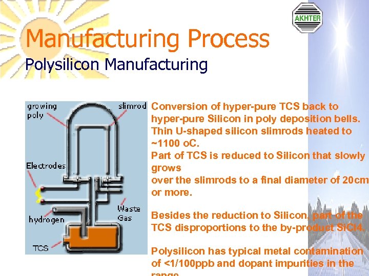
Manufacturing Process Polysilicon Manufacturing Conversion of hyper-pure TCS back to hyper-pure Silicon in poly deposition bells. Thin U-shaped silicon slimrods heated to ~1100 o. C. Part of TCS is reduced to Silicon that slowly grows over the slimrods to a final diameter of 20 cm or more. Besides the reduction to Silicon, part of the TCS disproportions to the by-product Si. Cl 4. Polysilicon has typical metal contamination of <1/100 ppb and dopant impurities in the
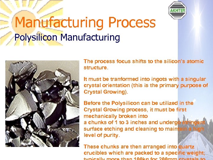
Manufacturing Process Polysilicon Manufacturing The process focus shifts to the silicon’s atomic structure. It must be tranformed into ingots with a singular crystal orientation (this is the primary purpose of Crystal Growing). Before the Polysilicon can be utilized in the Crystal Growing process, it must be first mechanically broken into a chunks of 1 to 3 inches and undergo stringent surface etching and cleaning to maintain a high level of purity. These chunks are then arranged into quartz crucibles which are packed to a specific weight;
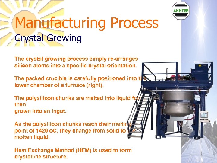
Manufacturing Process Crystal Growing The crystal growing process simply re-arranges silicon atoms into a specific crystal orientation. The packed crucible is carefully positioned into the lower chamber of a furnace (right). The polysilicon chunks are melted into liquid form, then grown into an ingot. As the polysilicon chunks reach their melting point of 1420 o. C, they change from solid to hot molten liquid. Heat Exchange Method (HEM) is used to form crystalline structure.
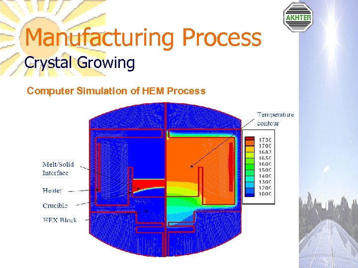
Manufacturing Process Crystal Growing Computer Simulation of HEM Process
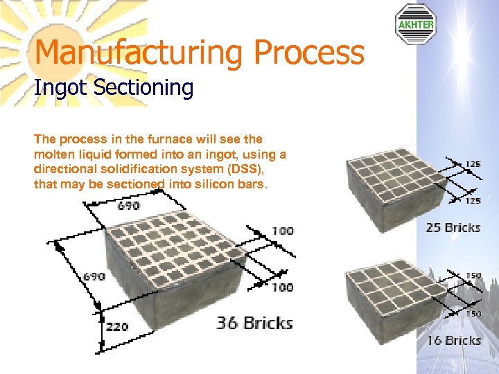
Manufacturing Process Ingot Sectioning The process in the furnace will see the molten liquid formed into an ingot, using a directional solidification system (DSS), that may be sectioned into silicon bars.
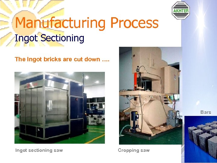
Manufacturing Process Ingot Sectioning The Ingot bricks are cut down …. Bars Ingot sectioning saw Cropping saw
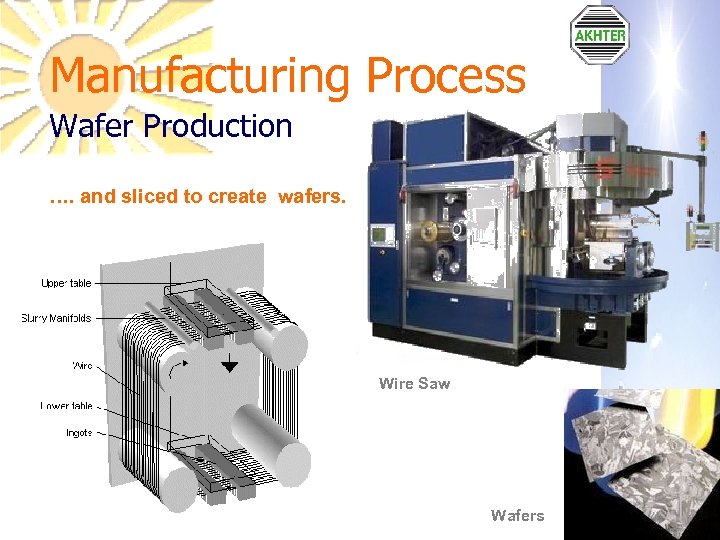
Manufacturing Process Wafer Production …. and sliced to create wafers. Wire Saw Wafers
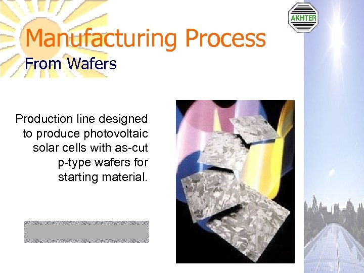
Manufacturing Process From Wafers Production line designed to produce photovoltaic solar cells with as-cut p-type wafers for starting material.
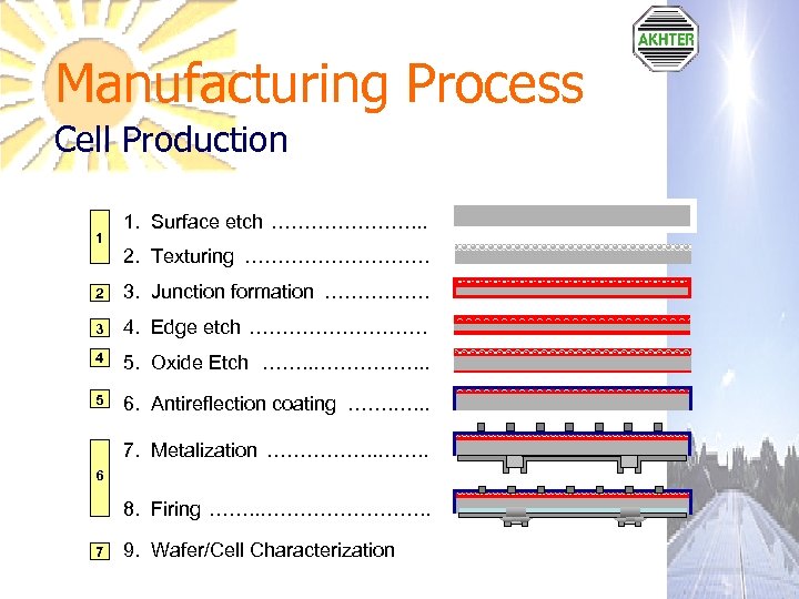
Manufacturing Process Cell Production 1 1. Surface etch …………………. . . 2. Texturing ……………. 2 3. Junction formation ……………. 3 4. Edge etch …………… 4 5. Oxide Etch ……. . ……………. . . 5 6. Antireflection coating ……. …. . . 7. Metalization ……………. . 6 8. Firing ……. . …………. . 7 9. Wafer/Cell Characterization
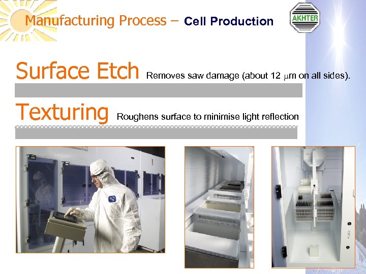
Manufacturing Process – Cell Production Surface Etch Texturing Removes saw damage (about 12 m on all sides). Roughens surface to minimise light reflection .
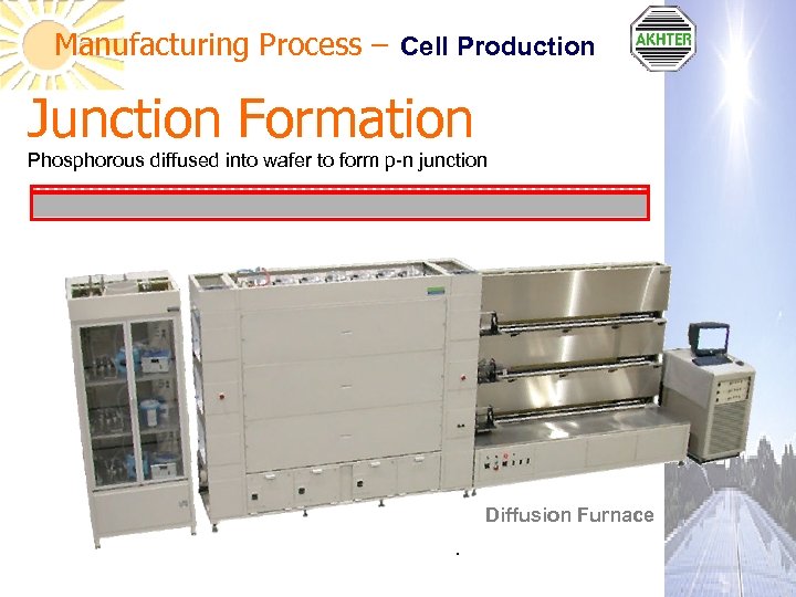
Manufacturing Process – Cell Production Junction Formation Phosphorous diffused into wafer to form p-n junction Diffusion Furnace.
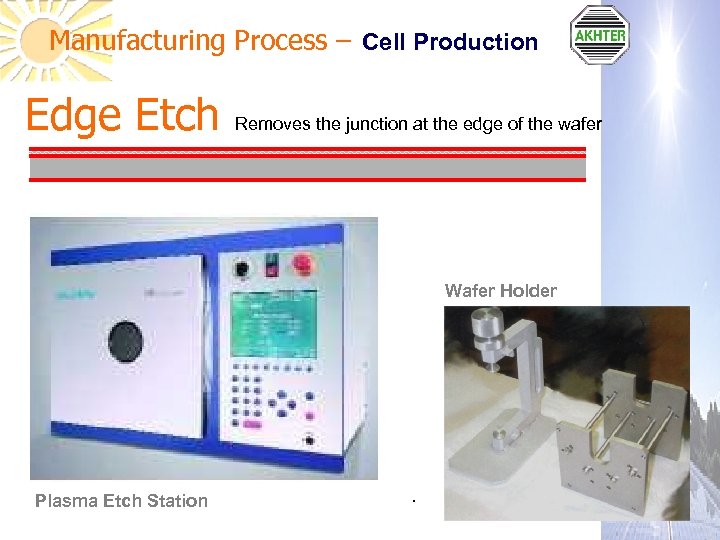
Manufacturing Process – Cell Production Edge Etch Removes the junction at the edge of the wafer Wafer Holder Plasma Etch Station .
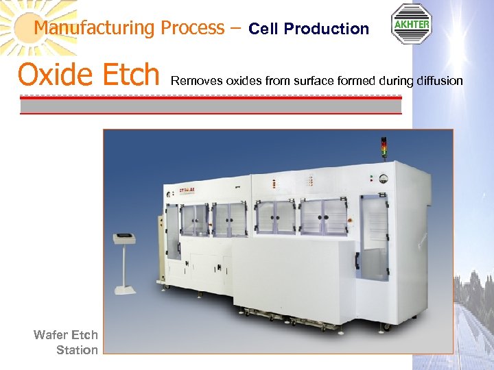
Manufacturing Process – Cell Production Oxide Etch Wafer Etch Station Removes oxides from surface formed during diffusion .
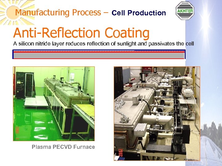
Manufacturing Process – Cell Production Anti-Reflection Coating A silicon nitride layer reduces reflection of sunlight and passivates the cell Plasma PECVD Furnace .
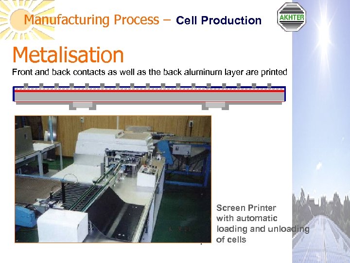
Manufacturing Process – Cell Production Metalisation Front and back contacts as well as the back aluminum layer are printed . Screen Printer with automatic loading and unloading of cells
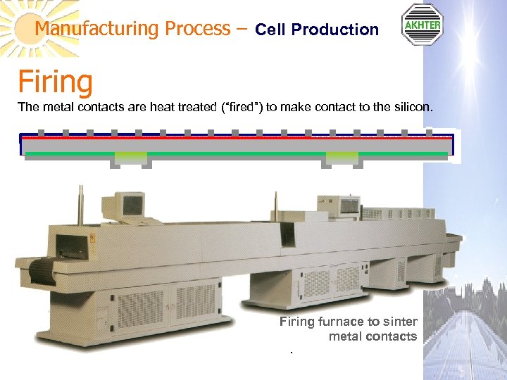
Manufacturing Process – Cell Production Firing The metal contacts are heat treated (“fired”) to make contact to the silicon. Firing furnace to sinter metal contacts.
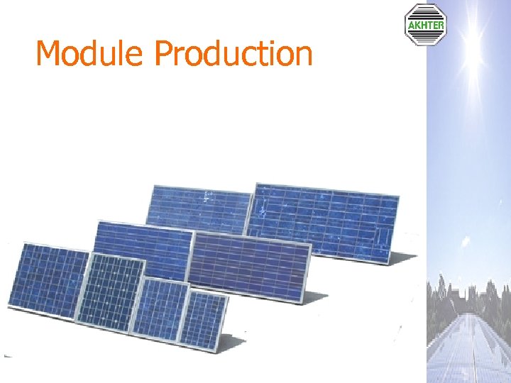
Module Production

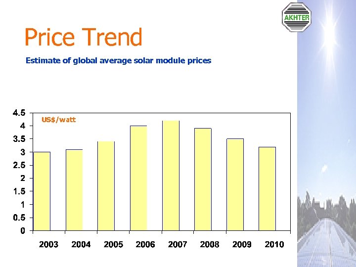
Price Trend Estimate of global average solar module prices US$/watt
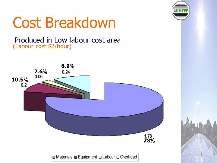
Cost Breakdown Produced in Low labour cost area (Labour cost $2/hour) 2. 6% 8. 9% 10. 5% 78%
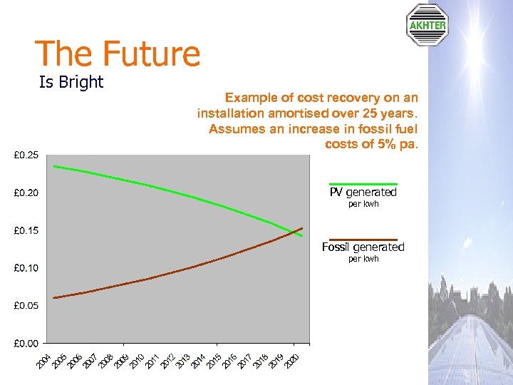
The Future Is Bright Example of cost recovery on an installation amortised over 25 years. Assumes an increase in fossil fuel costs of 5% pa. PV generated per kwh Fossil generated per kwh
Future Developments R&D is focused on increasing conversion efficiency and reducing cell manufacturing cost, to reduce electricity generation cost. • Improved crystallisation processes for high quality, low-cost silicon wafers • Advanced silicon solar cell device structures and manufacturing processes • Technology transfer of high efficiency solar cell processes from the laboratory to high volume production • Reduction of the silicon wafer thickness to reduce the consumption of silicon • Stable, high efficiency thin-film cells to reduce semiconductor materials costs • Novel organic and polymer solar cells with potentially low manufacturing cost • Solar concentrator systems using lenses or mirrors to focus the sunlight onto small-area, high-efficiency solar cells
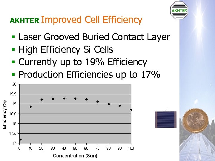
AKHTER Improved § § Cell Efficiency Laser Grooved Buried Contact Layer High Efficiency Si Cells Currently up to 19% Efficiency Production Efficiencies up to 17%
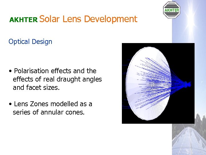
AKHTER Solar Lens Development Optical Design • Polarisation effects and the effects of real draught angles and facet sizes. • Lens Zones modelled as a series of annular cones.
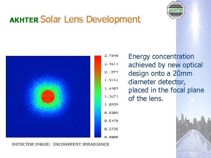
AKHTER Solar Lens Development Energy concentration achieved by new optical design onto a 20 mm diameter detector, placed in the focal plane of the lens. DETECTOR IMAGE: INCOHERENT IRRADIANCE
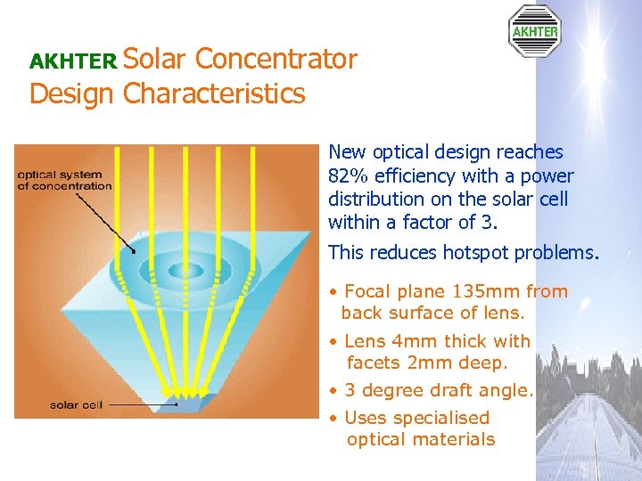
AKHTER Solar Concentrator Design Characteristics New optical design reaches 82% efficiency with a power distribution on the solar cell within a factor of 3. This reduces hotspot problems. • Focal plane 135 mm from back surface of lens. • Lens 4 mm thick with facets 2 mm deep. • 3 degree draft angle. • Uses specialised optical materials
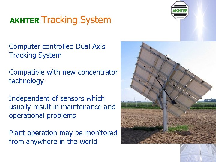
AKHTER Tracking System Computer controlled Dual Axis Tracking System Compatible with new concentrator technology Independent of sensors which usually result in maintenance and operational problems Plant operation may be monitored from anywhere in the world
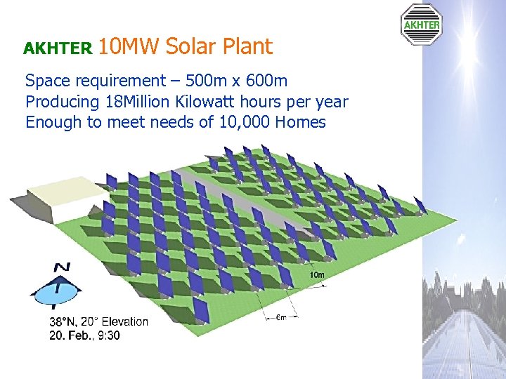
AKHTER 10 MW Solar Plant Space requirement – 500 m x 600 m Producing 18 Million Kilowatt hours per year Enough to meet needs of 10, 000 Homes
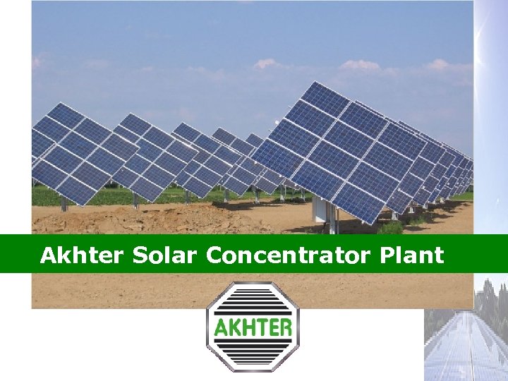
Akhter Solar Concentrator Plant

Thank you Professor Humayun A Mughal Chairman, Akhter Group PLC
c540da6d79f8f3a3757254416247cbdc.ppt