a440975cd974d485d34b6b4b6c4c7e36.ppt
- Количество слайдов: 17
Photonics Activities within Solid State Lab a) Sensors for Biomedical Applications b) Electroluminescence of Fe. Si 2 in Si c) Polymer Light Emitting Diodes Department of Electronic Engineering The Chinese University of Hong Kong March 17, 2000 M. Allard Research on Photonic Crystals
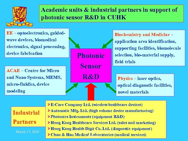
Academic units & industrial partners in support of photonic sensor R&D in CUHK EE – optoelectronics, guidedwave devices, biomedical electronics, signal processing, device fabrication ACAE – Centre for Micro and Nano Systems, MEMS, micro-fluidics, device modeling Industrial Partners March 17, 2000 Photonic Sensor R&D Biochemistry and Medicine – application area identification, supporting facilities, biomolecule selection, bio-material supply, field trials Physics – laser optics, optical diagnostic facilities, novel materials ØE-Care Company Ltd. (wireless healthcare devices) ØAutomatic Mfg. Ltd. (high volume device manufacturing) ØPhotonics Instruments (equipment R&D) ØHong Kong Healthcare Services Ltd. (sales and marketing) ØHong Kong Health Digit Co. Ltd. (diagnostic equipment) M. Allard Research on Photonic ØChan & Hau Medical Laboratories (medical services) Crystals
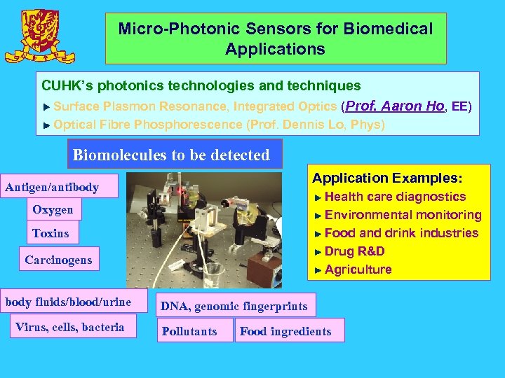
Micro-Photonic Sensors for Biomedical Applications CUHK’s photonics technologies and techniques Surface Plasmon Resonance, Integrated Optics (Prof. Aaron Ho, EE) Optical Fibre Phosphorescence (Prof. Dennis Lo, Phys) Biomolecules to be detected Application Examples: Antigen/antibody Health care diagnostics Environmental monitoring Food and drink industries Drug R&D Agriculture Oxygen Toxins Carcinogens body fluids/blood/urine Virus, cells, bacteria DNA, genomic fingerprints Pollutants Food ingredients
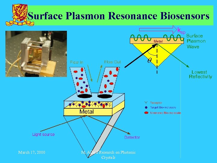
Surface Plasmon Resonance Biosensors ksp Metal Surface Plasmon Wave q Lowest Reflectivity March 17, 2000 M. Allard Research on Photonic Crystals
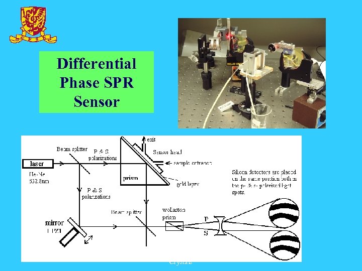
Differential Phase SPR Sensor March 17, 2000 M. Allard Research on Photonic Crystals
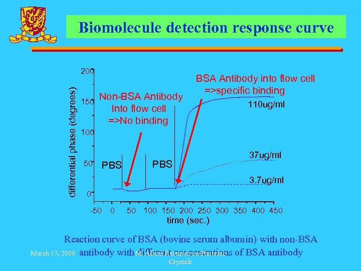
Biomolecule detection response curve differential phase (degrees) 200 150 Non-BSA Antibody Into flow cell =>No binding BSA Antibody into flow cell =>specific binding 110 ug/ml 100 50 PBS 37 ug/ml 3. 7 ug/ml 0 -50 0 50 100 150 200 250 300 350 400 450 time (sec. ) Reaction curve of BSA (bovine serum albumin) with non-BSA different concentrations March 17, 2000 antibody with M. Allard Research on Photonic of BSA antibody Crystals
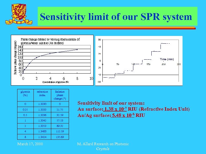
Relative phase change (degree) Sensitivity limit of our SPR system Phase change caused by varying concentration of glycerin/water mixture (Au surface) 160 140 120 100 80 60 40 20 0 0 Time (min) 2 4 6 8 10 Concentration of glycerin (%) refractive index Relative phase change (°) 0 1. 3330 0 0. 25 1. 3333 21. 75 0. 5 1. 3336 32. 59 1 1. 3342 57. 53 2 1. 3353 89. 32 4 1. 3400 112. 59 8 1. 3424 135. 69 March 17, 2000 Sensitivity limit of our system: Au surface: 1. 38 x 10 -7 RIU (Refractive Index Unit) Au/Ag surface: 5. 48 x 10 -8 RIU M. Allard Research on Photonic Crystals
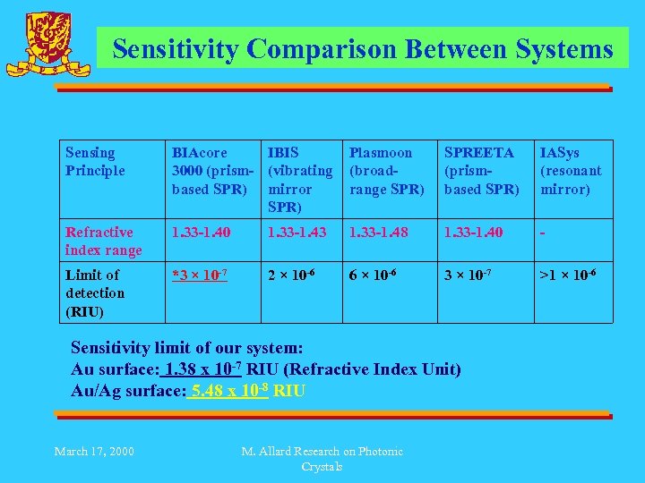
Sensitivity Comparison Between Systems Sensing Principle BIAcore IBIS 3000 (prism- (vibrating based SPR) mirror SPR) Plasmoon (broadrange SPR) SPREETA (prismbased SPR) IASys (resonant mirror) Refractive index range 1. 33 -1. 40 1. 33 -1. 43 1. 33 -1. 48 1. 33 -1. 40 - Limit of detection (RIU) *3 × 10 -7 2 × 10 -6 6 × 10 -6 3 × 10 -7 >1 × 10 -6 Sensitivity limit of our system: Au surface: 1. 38 x 10 -7 RIU (Refractive Index Unit) Au/Ag surface: 5. 48 x 10 -8 RIU March 17, 2000 M. Allard Research on Photonic Crystals
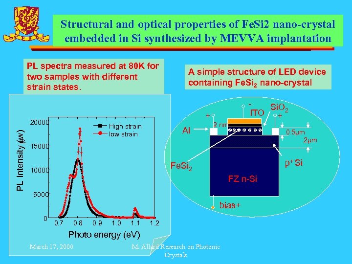
Structural and optical properties of Fe. Si 2 nano-crystal embedded in Si synthesized by MEVVA implantation PL spectra measured at 80 K for two samples with different strain states. Si. O ITO + 20000 PL Intensity mw) ( A simple structure of LED device containing Fe. Si 2 nano-crystal High strain low strain Al 2 nm 15000 p+ Si Fe. Si 2 10000 FZ n-Si 5000 bias+ 0 0. 7 0. 8 0. 9 1. 0 1. 1 1. 2 Photo energy (e. V) March 17, 2000 0. 5μm 2μm M. Allard Research on Photonic Crystals
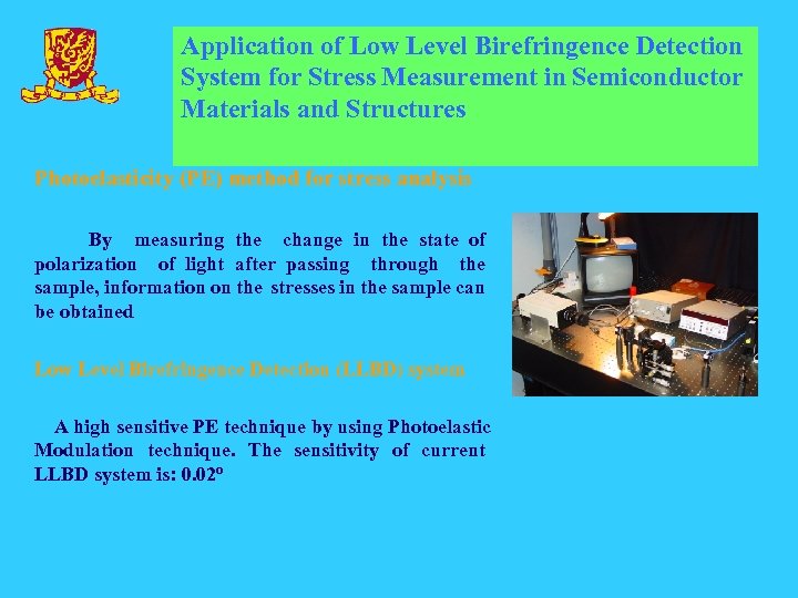
Application of Low Level Birefringence Detection System for Stress Measurement in Semiconductor Materials and Structures Photoelasticity (PE) method for stress analysis By measuring the change in the state of polarization of light after passing through the sample, information on the stresses in the sample can be obtained Low Level Birefringence Detection (LLBD) system A high sensitive PE technique by using Photoelastic Modulation technique. The sensitivity of current LLBD system is: 0. 02º
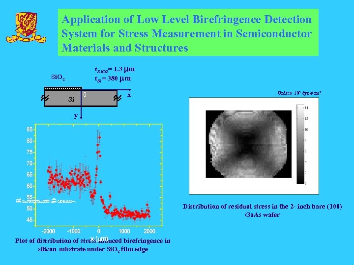
Application of Low Level Birefringence Detection System for Stress Measurement in Semiconductor Materials and Structures t. S i. O 2= 1. 3 m t. Si = 380 m Si. O 2 0 Si Unit: 107 dyne/cm 2 x y (1 1 0) Distribution of residual stress in the 2 - inch bare (100) Ga. As wafer Plot of distribution of stress induced birefringence in silicon substrate under Si. O 2 film edge
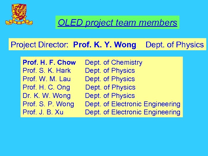
OLED project team members Project Director: Prof. K. Y. Wong Prof. H. F. Chow Prof. S. K. Hark Prof. W. M. Lau Prof. H. C. Ong Dr. K. W. Wong Prof. S. P. Wong Prof. J. B. Xu Dept. of Physics Dept. of Chemistry Dept. of Physics Dept. of Electronic Engineering
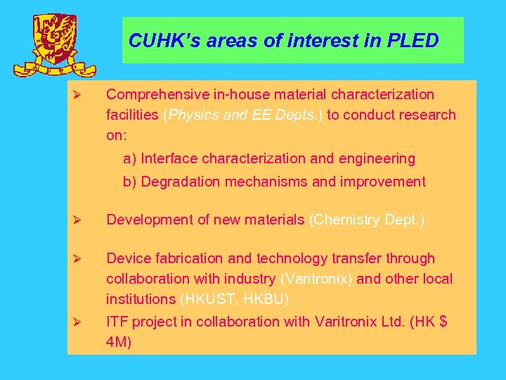
CUHK’s areas of interest in PLED Ø Comprehensive in-house material characterization facilities (Physics and EE Depts. ) to conduct research on: a) Interface characterization and engineering b) Degradation mechanisms and improvement Ø Development of new materials (Chemistry Dept. ) Ø Device fabrication and technology transfer through collaboration with industry (Varitronix) and other local institutions (HKUST, HKBU) Ø ITF project in collaboration with Varitronix Ltd. (HK $ 4 M)
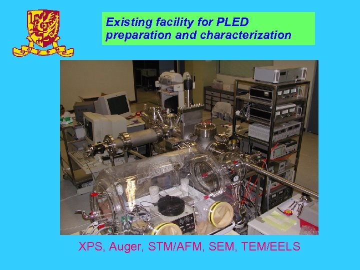
Existing facility for PLED preparation and characterization XPS, Auger, STM/AFM, SEM, TEM/EELS
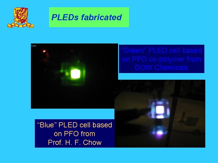
PLEDs fabricated “Green” PLED cell based on PFO co-polymer from DOW Chemicals “Blue” PLED cell based on PFO from Prof. H. F. Chow

END

March 17, 2000 M. Allard Research on Photonic Crystals
a440975cd974d485d34b6b4b6c4c7e36.ppt