eefeeff9f0acd46f8536fb3567686288.ppt
- Количество слайдов: 40
 Peripherals & Enhanced FLASH New Peripherals and Demo Enhanced FLASH PIC 16 F 87 X and PIC 16 F 62 X © 1999 Microchip Technology Incorporated. All Rights Reserved. S 4525 A Peripherals & Enhanced FLASH 1
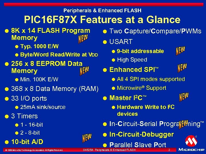 Peripherals & Enhanced FLASH PIC 16 F 87 X Features at a Glance l 8 K x 14 FLASH Program Memory l l l USART l l 10 -bit A/D © 1999 Microchip Technology Incorporated. All Rights Reserved. High Speed Enhanced SPIä l All 4 SPI modes supported l 25 m. A sink/source 1 - 16 -bit 2 - 8 -bit 9 -bit addressable l Min. 100 K E/W Microwire Support Master I 2 Cä l 3 Timers l l 368 x 8 Data Memory (RAM) 33 I/O ports l Two Capture/Compare/PWMs l 256 x 8 EEPROM Data Memory l l Typ. 1000 E/W Byte/Word Read/Write at VDD l Hardware Write to I 2 C devices l In-Circuit-Serial Programmingä l In-Circuit-Debugger l Parallel Slave Port S 4525 A Peripherals & Enhanced FLASH 2
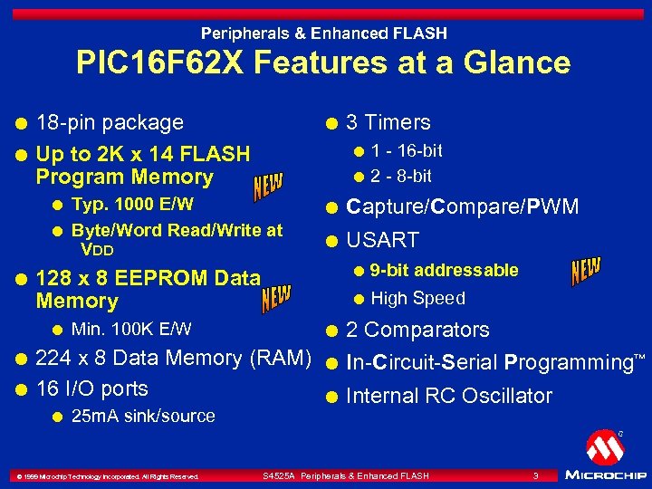 Peripherals & Enhanced FLASH PIC 16 F 62 X Features at a Glance l l 18 -pin package Up to 2 K x 14 FLASH Program Memory l l l Typ. 1000 E/W Byte/Word Read/Write at VDD l Capture/Compare/PWM l USART © 1999 Microchip Technology Incorporated. All Rights Reserved. 9 -bit addressable l High Speed l Min. 100 K E/W 25 m. A sink/source 1 - 16 -bit 2 - 8 -bit l 224 x 8 Data Memory (RAM) 16 I/O ports l 3 Timers l 128 x 8 EEPROM Data Memory l l l 2 Comparators l In-Circuit-Serial Programmingä l Internal RC Oscillator S 4525 A Peripherals & Enhanced FLASH 3
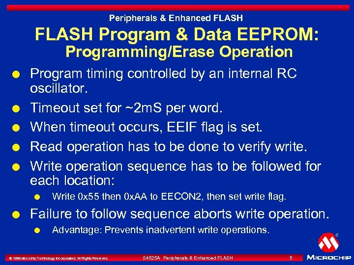 Peripherals & Enhanced FLASH Program & Data EEPROM: Programming/Erase Operation l l l Program timing controlled by an internal RC oscillator. Timeout set for ~2 m. S per word. When timeout occurs, EEIF flag is set. Read operation has to be done to verify write. Write operation sequence has to be followed for each location: l l Write 0 x 55 then 0 x. AA to EECON 2, then set write flag. Failure to follow sequence aborts write operation. l Advantage: Prevents inadvertent write operations. © 1999 Microchip Technology Incorporated. All Rights Reserved. S 4525 A Peripherals & Enhanced FLASH 5
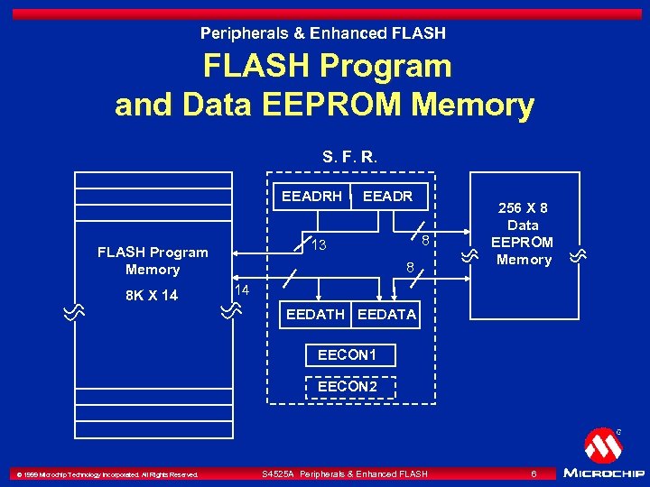 Peripherals & Enhanced FLASH Program and Data EEPROM Memory S. F. R. EEADRH 8 13 FLASH Program Memory 8 K X 14 EEADR 8 256 X 8 Data EEPROM Memory 14 EEDATH EEDATA EECON 1 EECON 2 © 1999 Microchip Technology Incorporated. All Rights Reserved. S 4525 A Peripherals & Enhanced FLASH 6
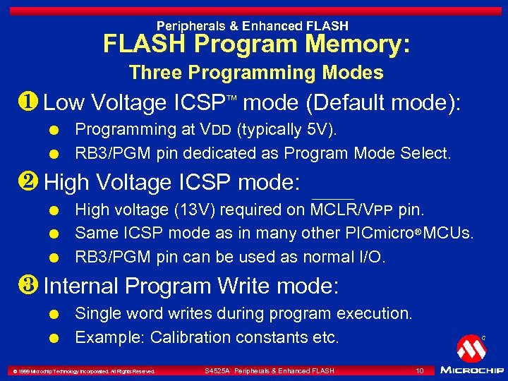 Peripherals & Enhanced FLASH Program Memory: Three Programming Modes ¶ Low Voltage ICSPä mode (Default mode): l l Programming at VDD (typically 5 V). RB 3/PGM pin dedicated as Program Mode Select. · High Voltage ICSP mode: l l l High voltage (13 V) required on MCLR/VPP pin. Same ICSP mode as in many other PICmicro® MCUs. RB 3/PGM pin can be used as normal I/O. ¸ Internal Program Write mode: l l Single word writes during program execution. Example: Calibration constants etc. © 1999 Microchip Technology Incorporated. All Rights Reserved. S 4525 A Peripherals & Enhanced FLASH 10
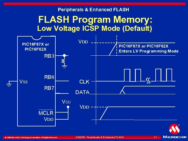 Peripherals & Enhanced FLASH Program Memory: Low Voltage ICSP Mode (Default) VDD PIC 16 F 87 X or PIC 16 F 62 X RB 3 VSS RB 6 PIC 16 F 87 X or PIC 16 F 62 X Enters LV Programming Mode CLK RB 7 DATA VDD MCLR VDD © 1999 Microchip Technology Incorporated. All Rights Reserved. S 4525 A Peripherals & Enhanced FLASH 11
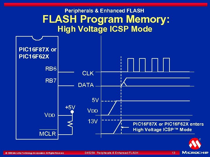 Peripherals & Enhanced FLASH Program Memory: High Voltage ICSP Mode PIC 16 F 87 X or PIC 16 F 62 X RB 6 CLK RB 7 DATA 5 V +5 V VDD MCLR © 1999 Microchip Technology Incorporated. All Rights Reserved. VDD 13 V PIC 16 F 87 X or PIC 16 F 62 X enters High Voltage ICSP™ Mode S 4525 A Peripherals & Enhanced FLASH 13
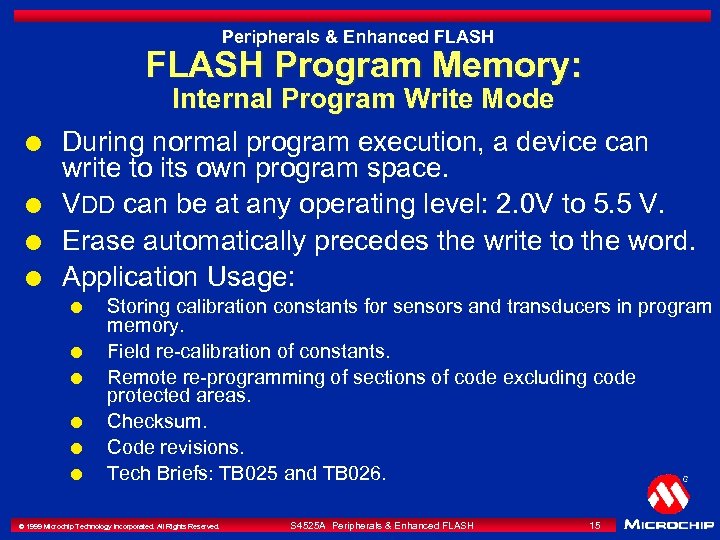 Peripherals & Enhanced FLASH Program Memory: l l Internal Program Write Mode During normal program execution, a device can write to its own program space. VDD can be at any operating level: 2. 0 V to 5. 5 V. Erase automatically precedes the write to the word. Application Usage: l l l Storing calibration constants for sensors and transducers in program memory. Field re-calibration of constants. Remote re-programming of sections of code excluding code protected areas. Checksum. Code revisions. Tech Briefs: TB 025 and TB 026. © 1999 Microchip Technology Incorporated. All Rights Reserved. S 4525 A Peripherals & Enhanced FLASH 15
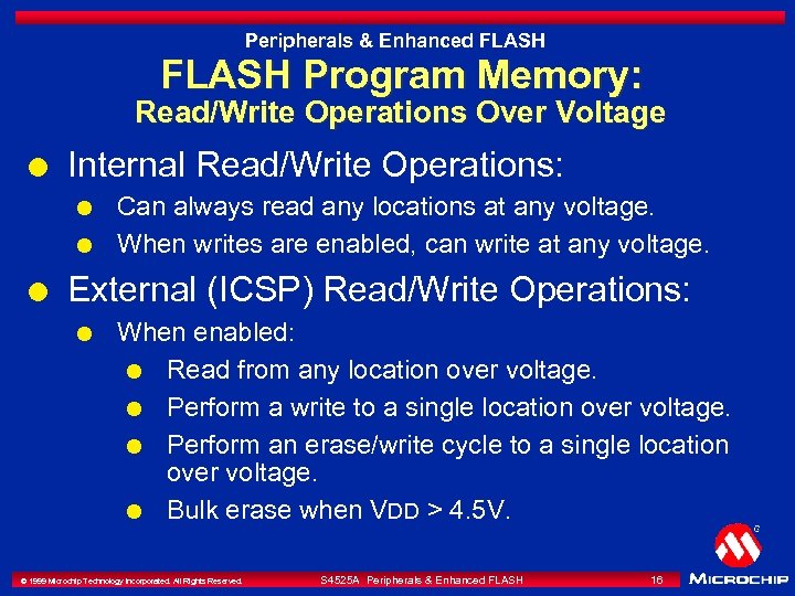 Peripherals & Enhanced FLASH Program Memory: Read/Write Operations Over Voltage l Internal Read/Write Operations: l l l Can always read any locations at any voltage. When writes are enabled, can write at any voltage. External (ICSP) Read/Write Operations: l When enabled: l Read from any location over voltage. l Perform a write to a single location over voltage. l Perform an erase/write cycle to a single location over voltage. l Bulk erase when VDD > 4. 5 V. © 1999 Microchip Technology Incorporated. All Rights Reserved. S 4525 A Peripherals & Enhanced FLASH 16
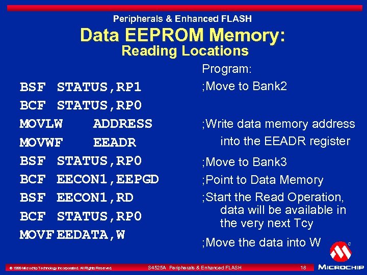 Peripherals & Enhanced FLASH Data EEPROM Memory: Reading Locations BSF STATUS, RP 1 BCF STATUS, RP 0 MOVLW ADDRESS MOVWF EEADR BSF STATUS, RP 0 BCF EECON 1, EEPGD BSF EECON 1, RD BCF STATUS, RP 0 MOVF EEDATA, W © 1999 Microchip Technology Incorporated. All Rights Reserved. Program: ; Move to Bank 2 ; Write data memory address into the EEADR register ; Move to Bank 3 ; Point to Data Memory ; Start the Read Operation, data will be available in the very next Tcy ; Move the data into W S 4525 A Peripherals & Enhanced FLASH 18
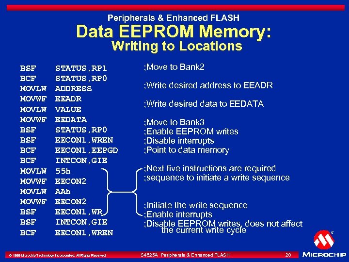 Peripherals & Enhanced FLASH Data EEPROM Memory: Writing to Locations BSF BCF MOVLW MOVWF BSF BSF BCF STATUS, RP 1 STATUS, RP 0 ADDRESS EEADR VALUE EEDATA STATUS, RP 0 EECON 1, WREN EECON 1, EEPGD INTCON, GIE 55 h EECON 2 AAh EECON 2 EECON 1, WR INTCON, GIE EECON 1, WREN © 1999 Microchip Technology Incorporated. All Rights Reserved. ; Move to Bank 2 ; Write desired address to EEADR ; Write desired data to EEDATA ; Move to Bank 3 ; Enable EEPROM writes ; Disable interrupts ; Point to data memory ; Next five instructions are required ; sequence to initiate a write sequence ; Initiate the write sequence ; Enable interrupts ; Disable EEPROM writes, does not affect the current write cycle S 4525 A Peripherals & Enhanced FLASH 20
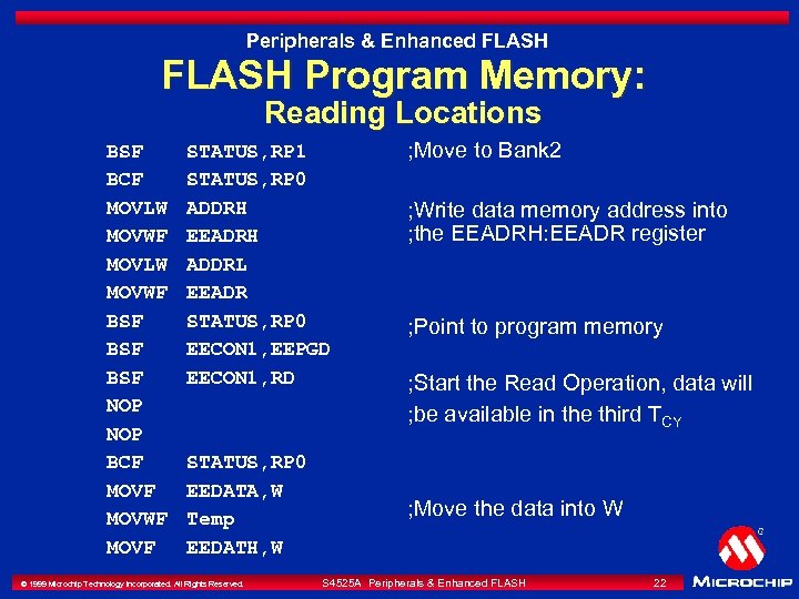 Peripherals & Enhanced FLASH Program Memory: Reading Locations BSF BCF MOVLW MOVWF BSF BSF NOP BCF MOVWF MOVF STATUS, RP 1 STATUS, RP 0 ADDRH EEADRH ADDRL EEADR STATUS, RP 0 EECON 1, EEPGD EECON 1, RD STATUS, RP 0 EEDATA, W Temp EEDATH, W © 1999 Microchip Technology Incorporated. All Rights Reserved. ; Move to Bank 2 ; Write data memory address into ; the EEADRH: EEADR register ; Point to program memory ; Start the Read Operation, data will ; be available in the third TCY ; Move the data into W S 4525 A Peripherals & Enhanced FLASH 22
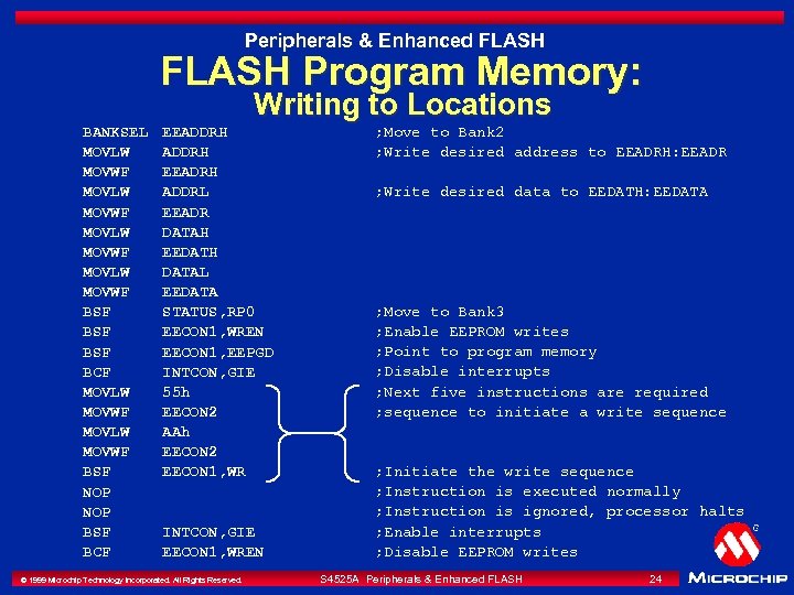 Peripherals & Enhanced FLASH Program Memory: Writing to Locations BANKSEL MOVLW MOVWF BSF BSF BCF MOVLW MOVWF BSF NOP BSF BCF EEADDRH EEADRH ADDRL EEADR DATAH EEDATH DATAL EEDATA STATUS, RP 0 EECON 1, WREN EECON 1, EEPGD INTCON, GIE 55 h EECON 2 AAh EECON 2 EECON 1, WR INTCON, GIE EECON 1, WREN © 1999 Microchip Technology Incorporated. All Rights Reserved. ; Move to Bank 2 ; Write desired address to EEADRH: EEADR ; Write desired data to EEDATH: EEDATA ; Move to Bank 3 ; Enable EEPROM writes ; Point to program memory ; Disable interrupts ; Next five instructions are required ; sequence to initiate a write sequence ; Initiate the write sequence ; Instruction is executed normally ; Instruction is ignored, processor halts ; Enable interrupts ; Disable EEPROM writes S 4525 A Peripherals & Enhanced FLASH 24
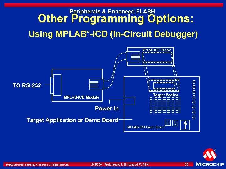 Peripherals & Enhanced FLASH Other Programming Options: Using MPLABä-ICD (In-Circuit Debugger) MPLAB-ICD Header TO RS-232 Target Socket. . . . . . . . . . . . . . MPLAB-ICD Module Power In Target Application or Demo Board MPLAB-ICD Demo Board © 1999 Microchip Technology Incorporated. All Rights Reserved. S 4525 A Peripherals & Enhanced FLASH 25
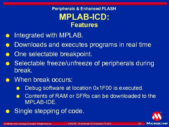 Peripherals & Enhanced FLASH MPLAB-ICD: Features l l l Integrated with MPLAB. Downloads and executes programs in real time One selectable breakpoint. Selectable freeze/unfreeze of peripherals during break. When break occurs: l l l Debug software at location 0 x 1 F 00 is executed. Contents of RAM or SFRs can be downloaded to the MPLAB-IDE. Single stepping of code. © 1999 Microchip Technology Incorporated. All Rights Reserved. S 4525 A Peripherals & Enhanced FLASH 26
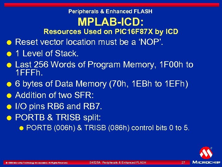 Peripherals & Enhanced FLASH MPLAB-ICD: Resources Used on PIC 16 F 87 X by ICD l l l l Reset vector location must be a ‘NOP’. 1 Level of Stack. Last 256 Words of Program Memory, 1 F 00 h to 1 FFFh. 6 bytes of Data Memory (70 h, 1 EBh to 1 EFh) Addition of two SFR: I/O pins RB 6 and RB 7. PORTB & TRISB split: l PORTB (006 h) & TRISB (086 h) control bits 0 to 5. © 1999 Microchip Technology Incorporated. All Rights Reserved. S 4525 A Peripherals & Enhanced FLASH 27
 Peripherals & Enhanced FLASH Reading FLASH Program Memory: Exercise 1 l l l Access a 7 -bit ASCII table without using the RETLW K instruction. Message located at location 0 x 500 is: “ Microchip PIC 16 F 87 X Demo. ” New MPASM directive {DA “Message”} is used to place the message in program memory. Message will be retrieved using the FLASH Read operation. Message will be displayed on the 16 x 2 Dot Matrix LCD. © 1999 Microchip Technology Incorporated. All Rights Reserved. S 4525 A Peripherals & Enhanced FLASH 28
 Peripherals & Enhanced FLASH Addressable USART: Address Feature l l Asynchronous mode, 9 -bit reception. When ADDEN = 1: l l RX 9 = 1 indicates an address byte. l RSR contents transferred to RCREG FIFO. l Receive interrupt flag set. RX 9 = 0 indicates a data byte. l Reception is ignored. l Interrupt flag not set, next reception overwrites byte. © 1999 Microchip Technology Incorporated. All Rights Reserved. S 4525 A Peripherals & Enhanced FLASH 29
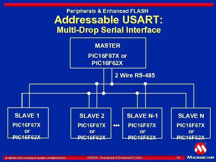 Peripherals & Enhanced FLASH Addressable USART: Multi-Drop Serial Interface MASTER PIC 16 F 87 X or PIC 16 F 62 X 2 Wire RS-485 SLAVE 1 SLAVE 2 PIC 16 F 87 X or PIC 16 F 62 X © 1999 Microchip Technology Incorporated. All Rights Reserved. SLAVE N-1 • • • SLAVE N PIC 16 F 87 X or PIC 16 F 62 X S 4525 A Peripherals & Enhanced FLASH 30
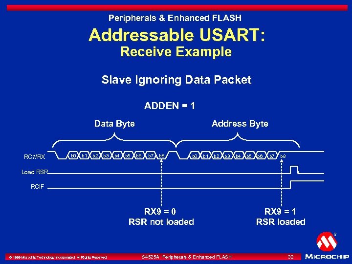 Peripherals & Enhanced FLASH Addressable USART: Receive Example Slave Ignoring Data Packet ADDEN = 1 Data Byte RC 7/RX b 0 b 1 b 2 b 3 b 4 b 5 Address Byte b 6 b 7 b 8 b 0 b 1 b 2 b 3 b 4 b 5 b 6 b 7 b 8 Load RSR RCIF RX 9 = 0 RSR not loaded © 1999 Microchip Technology Incorporated. All Rights Reserved. S 4525 A Peripherals & Enhanced FLASH RX 9 = 1 RSR loaded 32
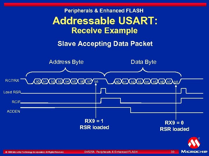 Peripherals & Enhanced FLASH Addressable USART: Receive Example Slave Accepting Data Packet Address Byte RC 7/RX b 0 b 1 b 2 b 3 b 4 b 5 b 6 Data Byte b 7 b 8 b 0 b 1 b 2 b 3 b 4 b 5 b 6 b 7 b 8 Load RSR RCIF ADDEN RX 9 = 1 RSR loaded © 1999 Microchip Technology Incorporated. All Rights Reserved. S 4525 A Peripherals & Enhanced FLASH RX 9 = 0 RSR loaded 33
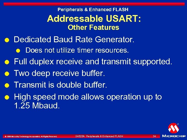 Peripherals & Enhanced FLASH Addressable USART: Other Features l Dedicated Baud Rate Generator. l l l Does not utilize timer resources. Full duplex receive and transmit supported. Two deep receive buffer. Transmit is double buffer. High speed mode allows operation up to 1. 25 Mbaud. © 1999 Microchip Technology Incorporated. All Rights Reserved. S 4525 A Peripherals & Enhanced FLASH 34
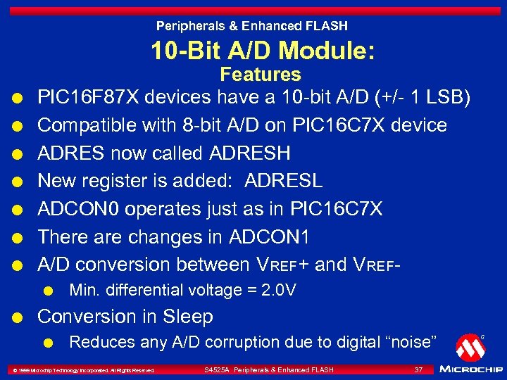 Peripherals & Enhanced FLASH 10 -Bit A/D Module: l l l l Features PIC 16 F 87 X devices have a 10 -bit A/D (+/- 1 LSB) Compatible with 8 -bit A/D on PIC 16 C 7 X device ADRES now called ADRESH New register is added: ADRESL ADCON 0 operates just as in PIC 16 C 7 X There are changes in ADCON 1 A/D conversion between VREF+ and VREFl l Min. differential voltage = 2. 0 V Conversion in Sleep l Reduces any A/D corruption due to digital “noise” © 1999 Microchip Technology Incorporated. All Rights Reserved. S 4525 A Peripherals & Enhanced FLASH 37
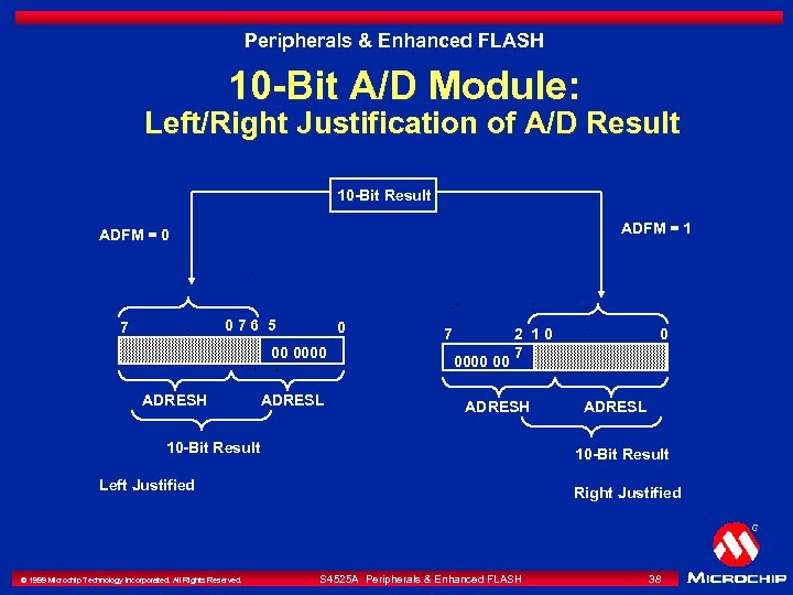 Peripherals & Enhanced FLASH 10 -Bit A/D Module: Left/Right Justification of A/D Result 10 -Bit Result ADFM = 1 ADFM = 0 076 5 7 0 00 0000 ADRESH ADRESL 7 0000 00 2 10 7 ADRESH 10 -Bit Result ADRESL 10 -Bit Result Left Justified © 1999 Microchip Technology Incorporated. All Rights Reserved. 0 Right Justified S 4525 A Peripherals & Enhanced FLASH 38
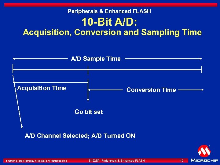 Peripherals & Enhanced FLASH 10 -Bit A/D: Acquisition, Conversion and Sampling Time A/D Sample Time Acquisition Time Conversion Time Go bit set A/D Channel Selected; A/D Turned ON © 1999 Microchip Technology Incorporated. All Rights Reserved. S 4525 A Peripherals & Enhanced FLASH 40
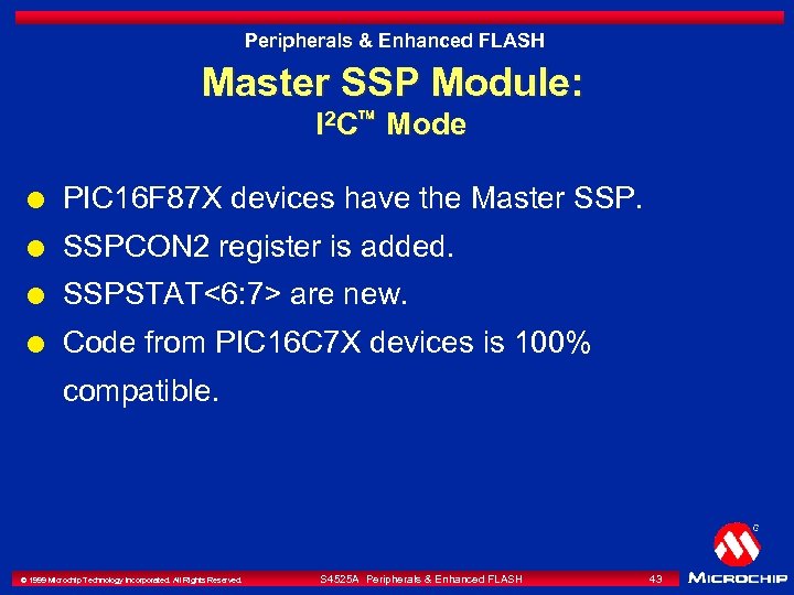 Peripherals & Enhanced FLASH Master SSP Module: I 2 Cä Mode l PIC 16 F 87 X devices have the Master SSP. l SSPCON 2 register is added. l SSPSTAT<6: 7> are new. l Code from PIC 16 C 7 X devices is 100% compatible. © 1999 Microchip Technology Incorporated. All Rights Reserved. S 4525 A Peripherals & Enhanced FLASH 43
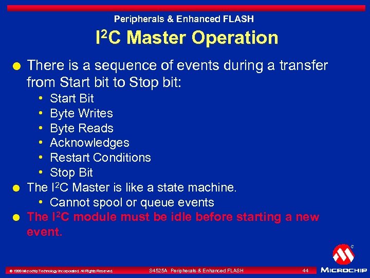 Peripherals & Enhanced FLASH I 2 C Master Operation l l l There is a sequence of events during a transfer from Start bit to Stop bit: • Start Bit • Byte Writes • Byte Reads • Acknowledges • Restart Conditions • Stop Bit The I 2 C Master is like a state machine. • Cannot spool or queue events The I 2 C module must be idle before starting a new event. © 1999 Microchip Technology Incorporated. All Rights Reserved. S 4525 A Peripherals & Enhanced FLASH 44
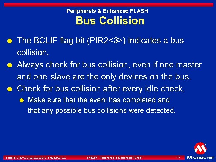 Peripherals & Enhanced FLASH Bus Collision l l l The BCLIF flag bit (PIR 2<3>) indicates a bus collision. Always check for bus collision, even if one master and one slave are the only devices on the bus. Check for bus collision after every idle check. l Make sure that the event has completed and that any possible bus collisions were detected. © 1999 Microchip Technology Incorporated. All Rights Reserved. S 4525 A Peripherals & Enhanced FLASH 47
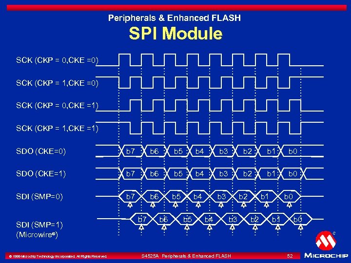 Peripherals & Enhanced FLASH SPI Module SCK (CKP = 0, CKE =0) SCK (CKP = 1, CKE =0) SCK (CKP = 0, CKE =1) SCK (CKP = 1, CKE =1) SDO (CKE=0) b 7 b 6 b 5 b 4 b 3 b 2 b 1 b 0 SDO (CKE=1) b 7 b 6 b 5 b 4 b 3 b 2 b 1 b 0 SDI (SMP=0) b 7 b 6 b 5 b 4 b 3 SDI (SMP=1) (Microwire®) © 1999 Microchip Technology Incorporated. All Rights Reserved. b 7 b 6 b 5 b 4 b 2 b 3 S 4525 A Peripherals & Enhanced FLASH b 1 b 2 b 0 b 1 b 0 52
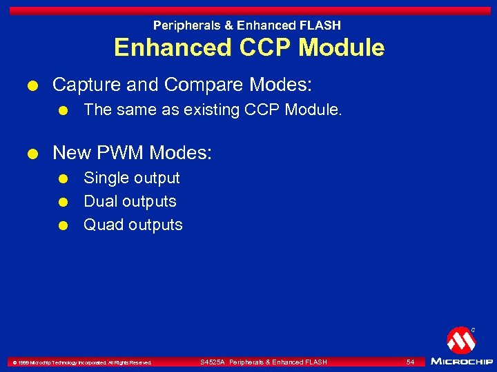 Peripherals & Enhanced FLASH Enhanced CCP Module l Capture and Compare Modes: l l The same as existing CCP Module. New PWM Modes: l l l Single output Dual outputs Quad outputs © 1999 Microchip Technology Incorporated. All Rights Reserved. S 4525 A Peripherals & Enhanced FLASH 54
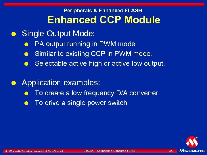 Peripherals & Enhanced FLASH Enhanced CCP Module l Single Output Mode: l l PA output running in PWM mode. Similar to existing CCP in PWM mode. Selectable active high or active low output. Application examples: l l To create a low frequency D/A converter. To drive a single power switch. © 1999 Microchip Technology Incorporated. All Rights Reserved. S 4525 A Peripherals & Enhanced FLASH 55
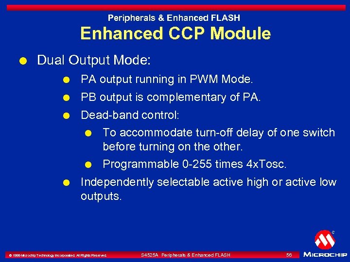 Peripherals & Enhanced FLASH Enhanced CCP Module l Dual Output Mode: l PA output running in PWM Mode. l PB output is complementary of PA. l Dead-band control: l l l To accommodate turn-off delay of one switch before turning on the other. Programmable 0 -255 times 4 x. Tosc. Independently selectable active high or active low outputs. © 1999 Microchip Technology Incorporated. All Rights Reserved. S 4525 A Peripherals & Enhanced FLASH 56
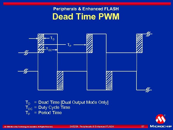 Peripherals & Enhanced FLASH Dead Time PWM TD TDC TP TD = Dead Time [Dual Output Mode Only] TDC = Duty Cycle Time TP = Period Time © 1999 Microchip Technology Incorporated. All Rights Reserved. S 4525 A Peripherals & Enhanced FLASH 57
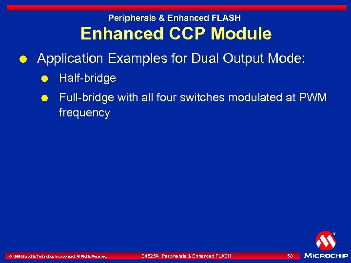 Peripherals & Enhanced FLASH Enhanced CCP Module l Application Examples for Dual Output Mode: l Half-bridge l Full-bridge with all four switches modulated at PWM frequency © 1999 Microchip Technology Incorporated. All Rights Reserved. S 4525 A Peripherals & Enhanced FLASH 58
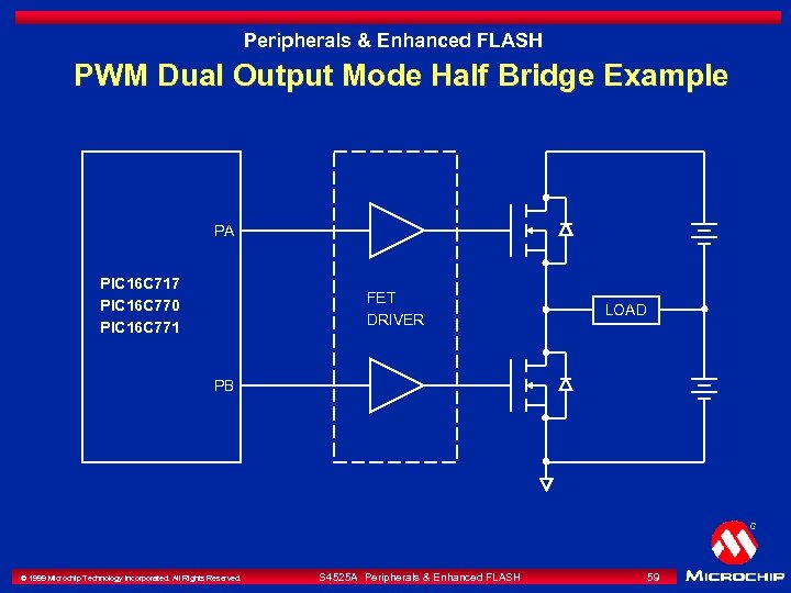 Peripherals & Enhanced FLASH PWM Dual Output Mode Half Bridge Example PA PIC 16 C 717 PIC 16 C 770 PIC 16 C 771 FET DRIVER LOAD PB © 1999 Microchip Technology Incorporated. All Rights Reserved. S 4525 A Peripherals & Enhanced FLASH 59
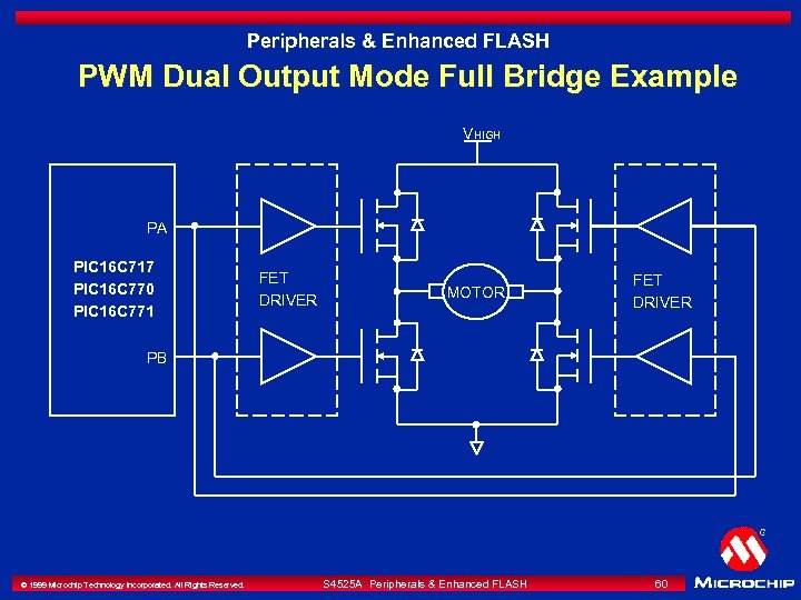 Peripherals & Enhanced FLASH PWM Dual Output Mode Full Bridge Example VHIGH PA PIC 16 C 717 PIC 16 C 770 PIC 16 C 771 FET DRIVER MOTOR FET DRIVER PB © 1999 Microchip Technology Incorporated. All Rights Reserved. S 4525 A Peripherals & Enhanced FLASH 60
 Peripherals & Enhanced FLASH Enhanced CCP Module l Quad Output Mode: l l PC or PA output is active. l l PB or PD output modulated. Independently selectable active high or active low output pairs. Application Examples: l Full-bridge where only one switch is modulated at PWM frequency to minimize switching losses. © 1999 Microchip Technology Incorporated. All Rights Reserved. S 4525 A Peripherals & Enhanced FLASH 61
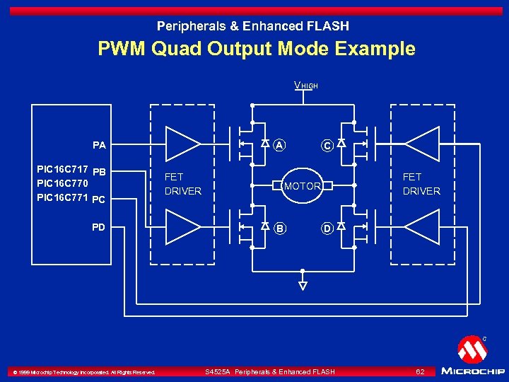 Peripherals & Enhanced FLASH PWM Quad Output Mode Example VHIGH PA PIC 16 C 717 PB PIC 16 C 770 PIC 16 C 771 PC PD © 1999 Microchip Technology Incorporated. All Rights Reserved. A FET DRIVER C FET DRIVER MOTOR B D S 4525 A Peripherals & Enhanced FLASH 62
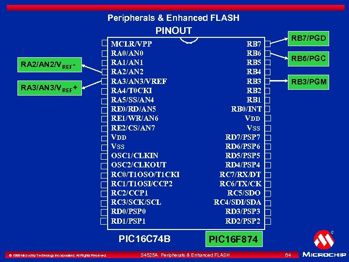 Peripherals & Enhanced FLASH PINOUT RA 2/AN 2/V REF RA 3/AN 3/V REF + MCLR/VPP RA 0/AN 0 RA 1/AN 1 RA 2/AN 2 RA 3/AN 3/VREF RA 4/T 0 CKI RA 5/SS/AN 4 RE 0/RD/AN 5 RE 1/WR/AN 6 RE 2/CS/AN 7 VDD VSS OSC 1/CLKIN OSC 2/CLKOUT RC 0/T 1 OSO/T 1 CKI RC 1/T 1 OSI/CCP 2 RC 2/CCP 1 RC 3/SCK/SCL RD 0/PSP 0 RD 1/PSP 1 PIC 16 C 74 B © 1999 Microchip Technology Incorporated. All Rights Reserved. RB 7/PGD RB 7 RB 6 RB 5 RB 4 RB 3 RB 2 RB 1 RB 0/INT VDD VSS RD 7/PSP 7 RD 6/PSP 6 RD 5/PSP 5 RD 4/PSP 4 RC 7/RX/DT RC 6/TX/CK RC 5/SDO RC 4/SDI/SDA RD 3/PSP 3 RD 2/PSP 2 RB 6/PGC RB 3/PGM PIC 16 F 874 S 4525 A Peripherals & Enhanced FLASH 64


