229518f7c4963382b016ddbc61cfc3d8.ppt
- Количество слайдов: 30
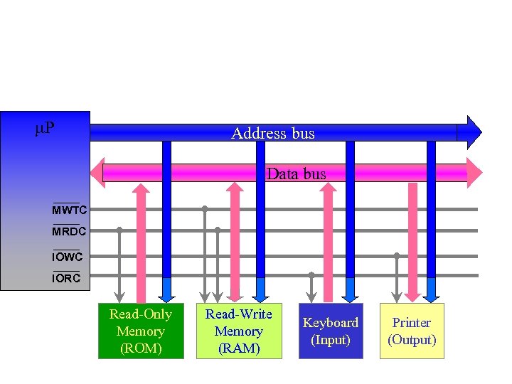
P Address bus Data bus MWTC MRDC IOWC IORC Read-Only Memory (ROM) Read-Write Memory (RAM) Keyboard (Input) Printer (Output)
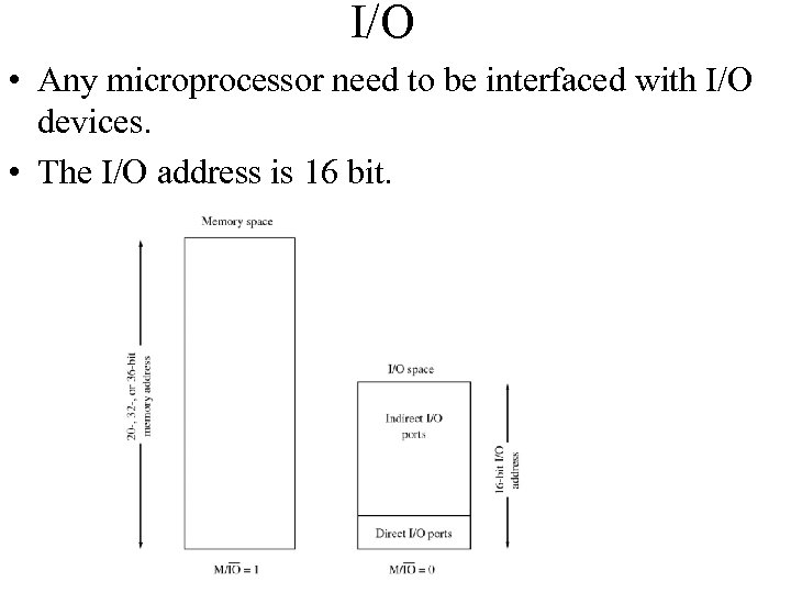
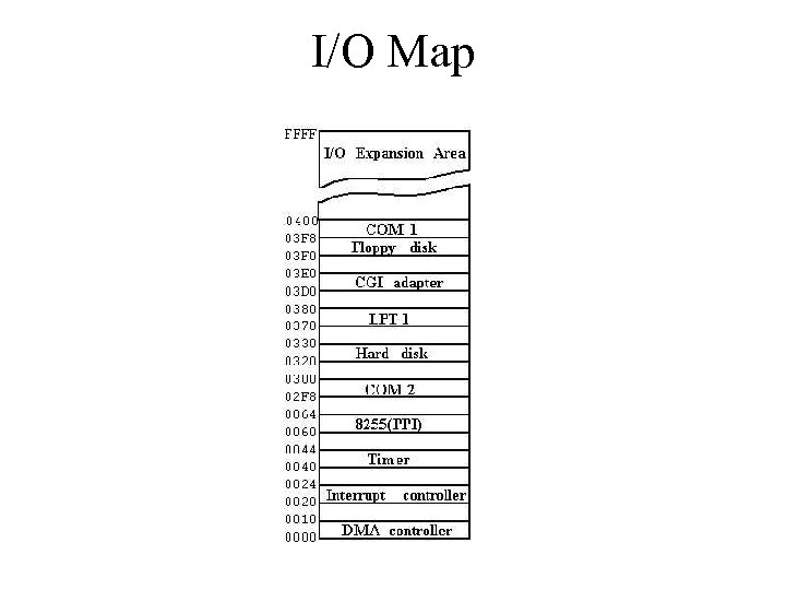
I/O • Any microprocessor need to be interfaced with I/O devices. • The I/O address is 16 bit.
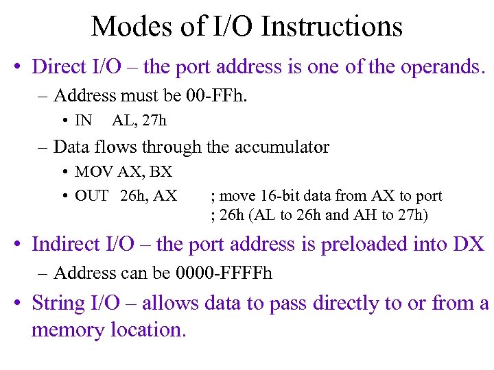
Modes of I/O Instructions • Direct I/O – the port address is one of the operands. – Address must be 00 -FFh. • IN AL, 27 h – Data flows through the accumulator • MOV AX, BX • OUT 26 h, AX ; move 16 -bit data from AX to port ; 26 h (AL to 26 h and AH to 27 h) • Indirect I/O – the port address is preloaded into DX – Address can be 0000 -FFFFh • String I/O – allows data to pass directly to or from a memory location.
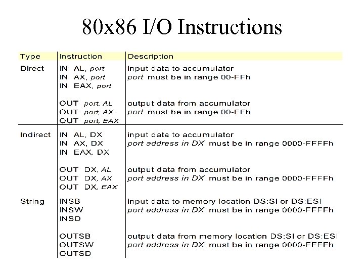
80 x 86 I/O Instructions
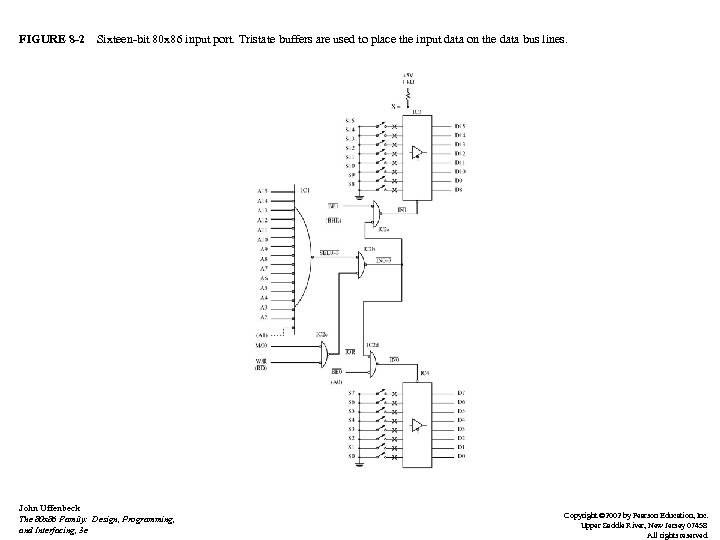
FIGURE 8 -2 Sixteen-bit 80 x 86 input port. Tristate buffers are used to place the input data on the data bus lines. John Uffenbeck The 80 x 86 Family: Design, Programming, and Interfacing, 3 e Copyright © 2002 by Pearson Education, Inc. Upper Saddle River, New Jersey 07458 All rights reserved.
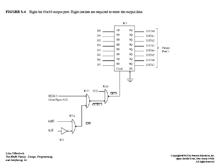
FIGURE 8 -4 Eight-bit 80 x 86 output port. Eight latches are required to store the output data. John Uffenbeck The 80 x 86 Family: Design, Programming, and Interfacing, 3 e Copyright © 2002 by Pearson Education, Inc. Upper Saddle River, New Jersey 07458 All rights reserved.
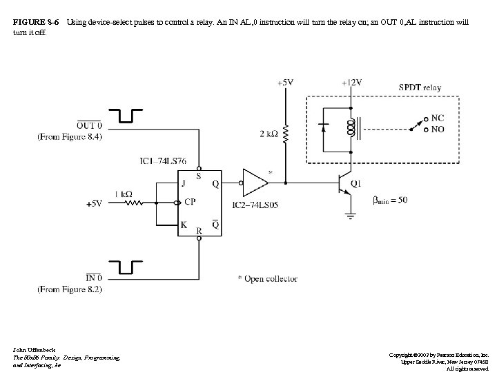
FIGURE 8 -6 Using device-select pulses to control a relay. An IN AL, 0 instruction will turn the relay on; an OUT 0, AL instruction will turn it off. John Uffenbeck The 80 x 86 Family: Design, Programming, and Interfacing, 3 e Copyright © 2002 by Pearson Education, Inc. Upper Saddle River, New Jersey 07458 All rights reserved.
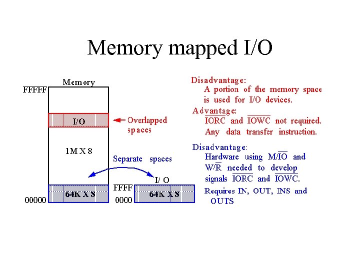
Memory mapped I/O
I/O Map
Programmed I/O
Parallel Printer Interface example
Parallel Printer Interface example
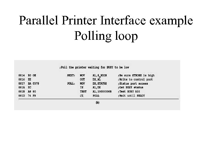
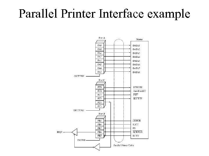
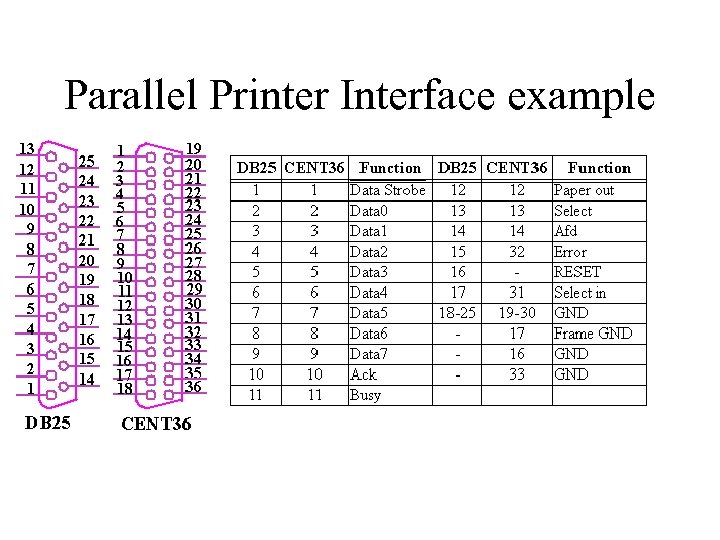
Parallel Printer Interface example Polling loop
Peripheral Controllers • Intel has developed several peripheral controller chips designed to support its processors. • The goal is to give a complete I/O interface in one chip. • Examples: • 8255 is Programmable Peripheral Interface (PPI). • 8259 is Programmable Interrupt Controller (PIC) • 8253/8254 is Programmable Interval Timer (PIT) • 8237 is Programmable DMA controller. • In PC/XT computers these chips are built into the system board and can be seen by inspection. • In modern Computers the functionality of these chips has been built into the system board chipset.
8255 A • Is one of the peripheral controller chips designed to support its processors. • 8255 is Programmable Peripheral Interface (PPI). • It is a general purpose parallel I/O Interfacing device. • It provides 24 I/O lines organized in three 8 -bit I/O ports in one 40 -pin package. • The ports are usually labeled A, B, and C. fig 8. 11
Size of ports • Ports A and B can be programmed as an 8 -bit input or output port. • In port C each nipple (four bits) can be programmed separately to be a 4 -bit input or output port. • Only the above size of ports (byte or nipple) can be programmed. For Example, individual bit in a port cannot be programmed. • However, what make 8254 a versatile devise is its programming modes
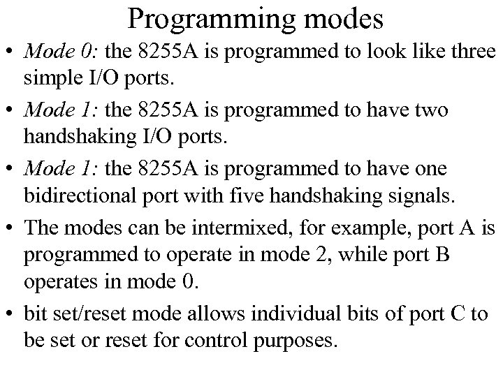
Programming modes • Mode 0: the 8255 A is programmed to look like three simple I/O ports. • Mode 1: the 8255 A is programmed to have two handshaking I/O ports. • Mode 1: the 8255 A is programmed to have one bidirectional port with five handshaking signals. • The modes can be intermixed, for example, port A is programmed to operate in mode 2, while port B operates in mode 0. • bit set/reset mode allows individual bits of port C to be set or reset for control purposes.
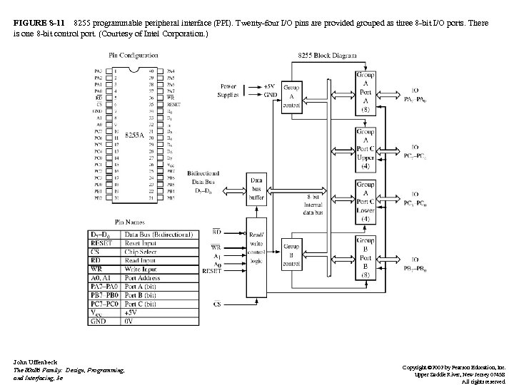
FIGURE 8 -11 8255 programmable peripheral interface (PPI). Twenty-four I/O pins are provided grouped as three 8 -bit I/O ports. There is one 8 -bit control port. (Courtesy of Intel Corporation. ) John Uffenbeck The 80 x 86 Family: Design, Programming, and Interfacing, 3 e Copyright © 2002 by Pearson Education, Inc. Upper Saddle River, New Jersey 07458 All rights reserved.
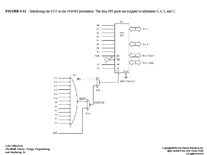
FIGURE 8 -12 Interfacing the 8255 to the 386/486 processors. The four PPI ports are mapped to addresses 0, 4, 8, and C. John Uffenbeck The 80 x 86 Family: Design, Programming, and Interfacing, 3 e Copyright © 2002 by Pearson Education, Inc. Upper Saddle River, New Jersey 07458 All rights reserved.
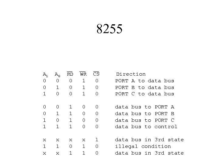
8255 A 1 0 0 1 A 0 0 1 0 RD 0 0 0 WR 1 1 1 CS 0 0 0 Direction PORT A to data bus PORT B to data bus PORT C to data bus 0 0 1 1 1 0 0 0 0 data x 1 x x 0 1 x 1 1 1 0 0 data bus in 3 rd state illegal condition data bus in 3 rd state bus bus to to PORT A PORT B PORT C control
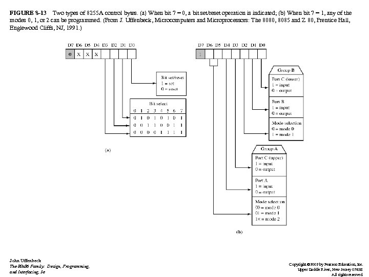
FIGURE 8 -13 Two types of 8255 A control bytes. (a) When bit 7 = 0, a bit set/reset operation is indicated; (b) When bit 7 = 1, any of the modes 0, 1, or 2 can be programmed. (From J. Uffenbeck, Microcomputers and Microprocessors: The 8080, 8085 and Z 80, Prentice Hall, Englewood Cliffs, NJ, 1991. ) John Uffenbeck The 80 x 86 Family: Design, Programming, and Interfacing, 3 e Copyright © 2002 by Pearson Education, Inc. Upper Saddle River, New Jersey 07458 All rights reserved.
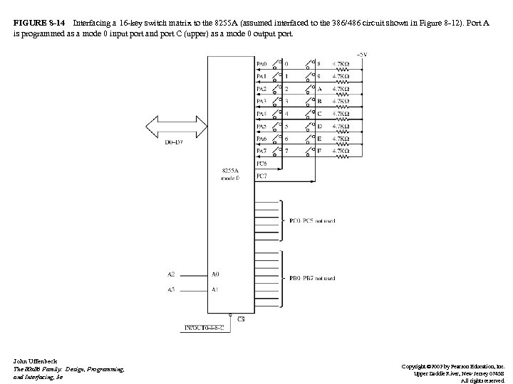
FIGURE 8 -14 Interfacing a 16 -key switch matrix to the 8255 A (assumed interfaced to the 386/486 circuit shown in Figure 8 -12). Port A is programmed as a mode 0 input port and port C (upper) as a mode 0 output port. John Uffenbeck The 80 x 86 Family: Design, Programming, and Interfacing, 3 e Copyright © 2002 by Pearson Education, Inc. Upper Saddle River, New Jersey 07458 All rights reserved.
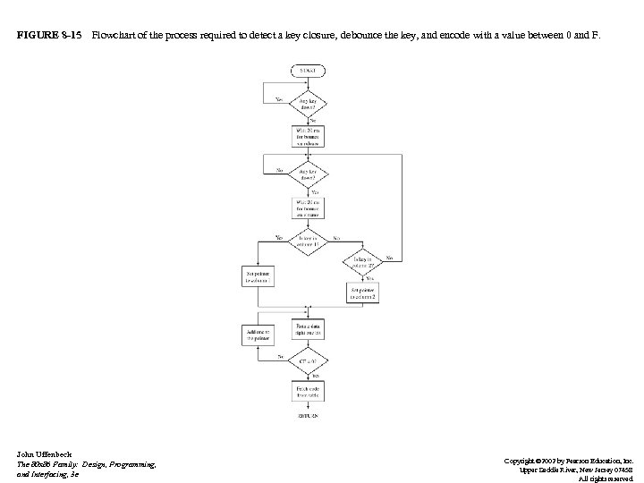
FIGURE 8 -15 Flowchart of the process required to detect a key closure, debounce the key, and encode with a value between 0 and F. John Uffenbeck The 80 x 86 Family: Design, Programming, and Interfacing, 3 e Copyright © 2002 by Pearson Education, Inc. Upper Saddle River, New Jersey 07458 All rights reserved.
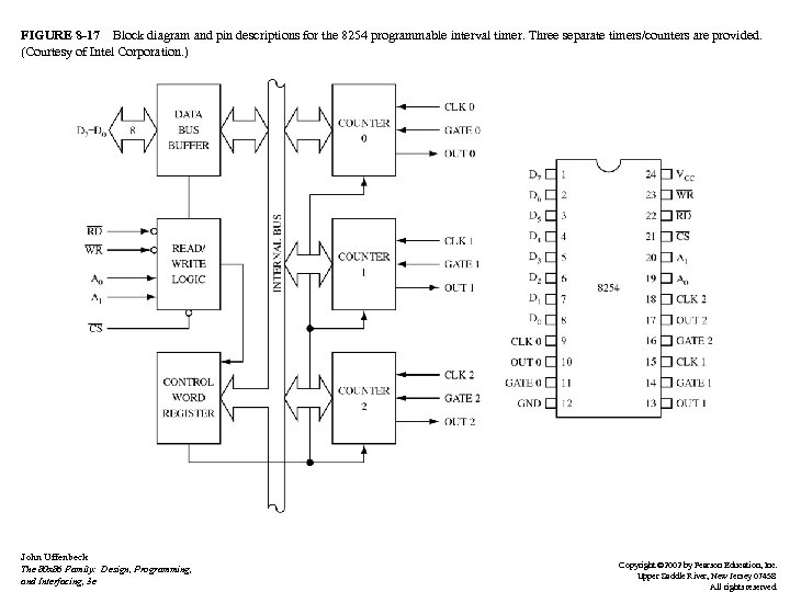
FIGURE 8 -17 Block diagram and pin descriptions for the 8254 programmable interval timer. Three separate timers/counters are provided. (Courtesy of Intel Corporation. ) John Uffenbeck The 80 x 86 Family: Design, Programming, and Interfacing, 3 e Copyright © 2002 by Pearson Education, Inc. Upper Saddle River, New Jersey 07458 All rights reserved.
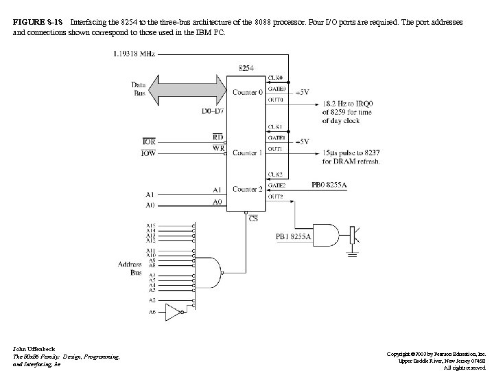
FIGURE 8 -18 Interfacing the 8254 to the three-bus architecture of the 8088 processor. Four I/O ports are required. The port addresses and connections shown correspond to those used in the IBM PC. John Uffenbeck The 80 x 86 Family: Design, Programming, and Interfacing, 3 e Copyright © 2002 by Pearson Education, Inc. Upper Saddle River, New Jersey 07458 All rights reserved.
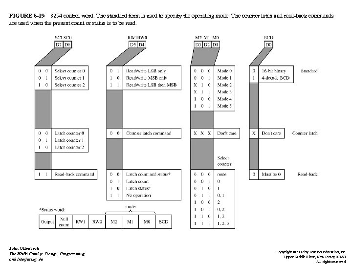
FIGURE 8 -19 8254 control word. The standard form is used to specify the operating mode. The counter latch and read-back commands are used when the present count or status is to be read. John Uffenbeck The 80 x 86 Family: Design, Programming, and Interfacing, 3 e Copyright © 2002 by Pearson Education, Inc. Upper Saddle River, New Jersey 07458 All rights reserved.
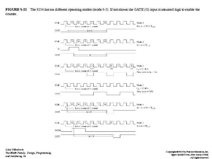
FIGURE 8 -22 The 8254 has six different operating modes (mode 0 -5). If not shown the GATE (G) input is assumed high to enable the counter. John Uffenbeck The 80 x 86 Family: Design, Programming, and Interfacing, 3 e Copyright © 2002 by Pearson Education, Inc. Upper Saddle River, New Jersey 07458 All rights reserved.
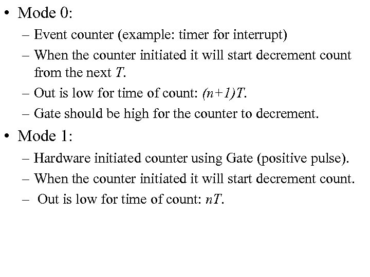
• Mode 0: – Event counter (example: timer for interrupt) – When the counter initiated it will start decrement count from the next T. – Out is low for time of count: (n+1)T. – Gate should be high for the counter to decrement. • Mode 1: – Hardware initiated counter using Gate (positive pulse). – When the counter initiated it will start decrement count. – Out is low for time of count: n. T.
• Mode 2: – The counter will generate a series of continuous pulses. – Out will pulse low for one period low at the end of the count. – f= clk/n duty cycle=(n-1)/n – Gate should be high. • Mode 3: – Square wave generator. – Like mode 2 – Half of the count, out is high and low in the other half.
• Mode 4: – The counter will generate a series of continuous pulses. – Out will have one active low pulse when at the end of the count. – out is high for (n+1)T and then one active low pulse – Gate should be high. • Mode 5: – Like mode 4 – But hardware imitated by Gate. – out is high for n. T and then one active low pulse
229518f7c4963382b016ddbc61cfc3d8.ppt