fb306b0141b4b0a6b9ba33c1b1764770.ppt
- Количество слайдов: 44
 Overview of the recent activities of the RD 50 collaboration on radiation hardening of semiconductor detectors for the SLHC G. Casse, Novosibirsk, 28/02 5/03 2008 10 th International Conference Instr. Colliding Beam Physics 1
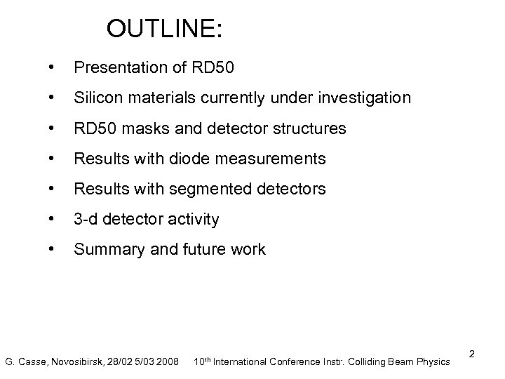 OUTLINE: • Presentation of RD 50 • Silicon materials currently under investigation • RD 50 masks and detector structures • Results with diode measurements • Results with segmented detectors • 3 -d detector activity • Summary and future work G. Casse, Novosibirsk, 28/02 5/03 2008 10 th International Conference Instr. Colliding Beam Physics 2
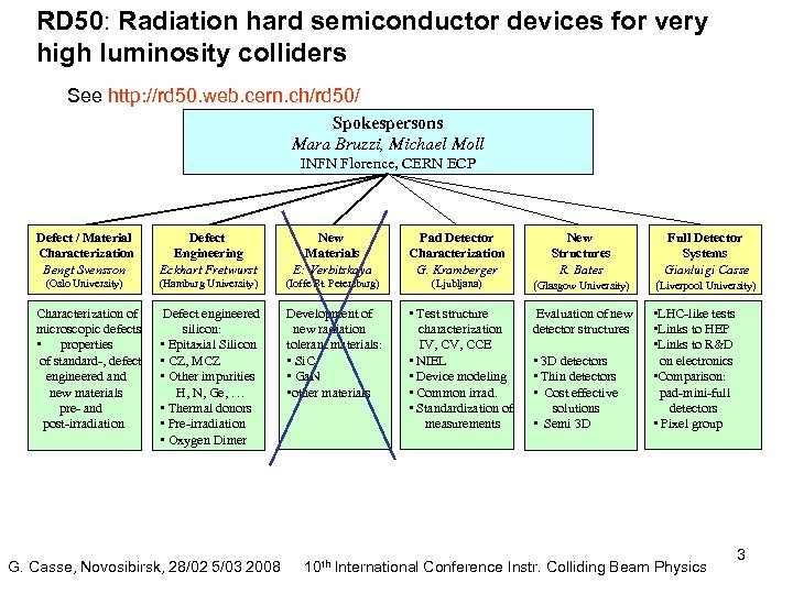 RD 50: Radiation hard semiconductor devices for very high luminosity colliders See http: //rd 50. web. cern. ch/rd 50/ Spokespersons Mara Bruzzi, Michael Moll INFN Florence, CERN ECP Defect / Material Characterization Bengt Svensson Defect Engineering Eckhart Fretwurst New Materials E: Verbitskaya Pad Detector Characterization G. Kramberger New Structures R. Bates Full Detector Systems Gianluigi Casse (Oslo University) (Hamburg University) (Ioffe St. Petersburg) (Ljubljana) (Glasgow University) (Liverpool University) Defect engineered silicon: • Epitaxial Silicon • CZ, MCZ • Other impurities H, N, Ge, … • Thermal donors • Pre-irradiation • Oxygen Dimer Development of new radiation tolerant materials: • Si. C • Ga. N • other materials Evaluation of new detector structures • LHC-like tests • Links to HEP • Links to R&D on electronics • Comparison: pad-mini-full detectors • Pixel group Characterization of microscopic defects • properties of standard-, defect engineered and new materials pre- and post-irradiation G. Casse, Novosibirsk, 28/02 5/03 2008 • Test structure characterization IV, CCE • NIEL • Device modeling • Common irrad. • Standardization of measurements • 3 D detectors • Thin detectors • Cost effective solutions • Semi 3 D 10 th International Conference Instr. Colliding Beam Physics 3
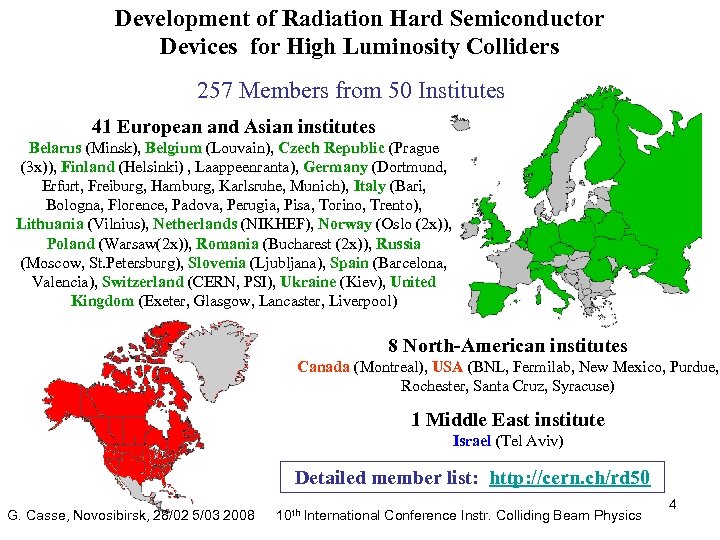 Development of Radiation Hard Semiconductor Devices for High Luminosity Colliders 257 Members from 50 Institutes 41 European and Asian institutes Belarus (Minsk), Belgium (Louvain), Czech Republic (Prague (3 x)), Finland (Helsinki) , Laappeenranta), Germany (Dortmund, Erfurt, Freiburg, Hamburg, Karlsruhe, Munich), Italy (Bari, Bologna, Florence, Padova, Perugia, Pisa, Torino, Trento), Lithuania (Vilnius), Netherlands (NIKHEF), Norway (Oslo (2 x)), Poland (Warsaw(2 x)), Romania (Bucharest (2 x)), Russia (Moscow, St. Petersburg), Slovenia (Ljubljana), Spain (Barcelona, Valencia), Switzerland (CERN, PSI), Ukraine (Kiev), United Kingdom (Exeter, Glasgow, Lancaster, Liverpool) 8 North-American institutes Canada (Montreal), USA (BNL, Fermilab, New Mexico, Purdue, Rochester, Santa Cruz, Syracuse) 1 Middle East institute Israel (Tel Aviv) Detailed member list: http: //cern. ch/rd 50 G. Casse, Novosibirsk, 28/02 5/03 2008 10 th International Conference Instr. Colliding Beam Physics 4
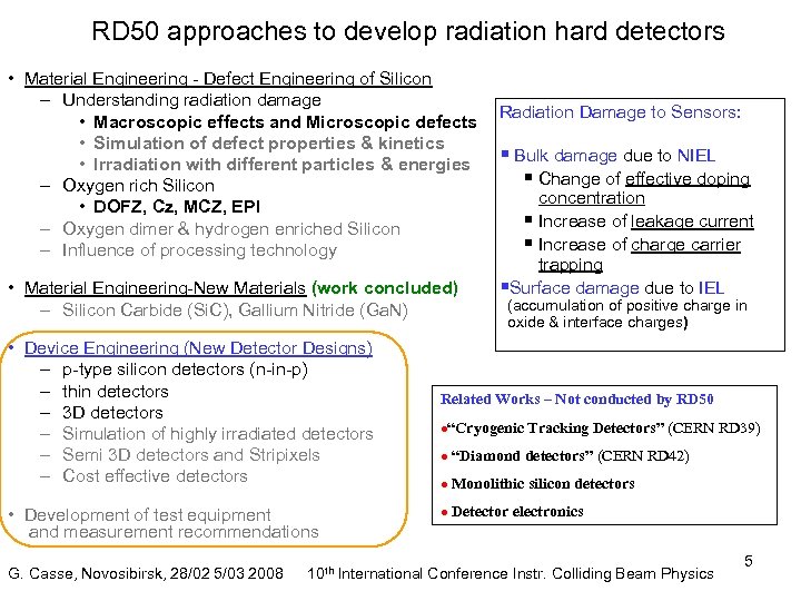 RD 50 approaches to develop radiation hard detectors • Material Engineering - Defect Engineering of Silicon – Understanding radiation damage • Macroscopic effects and Microscopic defects • Simulation of defect properties & kinetics • Irradiation with different particles & energies – Oxygen rich Silicon • DOFZ, Cz, MCZ, EPI – Oxygen dimer & hydrogen enriched Silicon – Influence of processing technology • Material Engineering-New Materials (work concluded) – Silicon Carbide (Si. C), Gallium Nitride (Ga. N) • Device Engineering (New Detector Designs) – p-type silicon detectors (n-in-p) – thin detectors – 3 D detectors – Simulation of highly irradiated detectors – Semi 3 D detectors and Stripixels – Cost effective detectors • Development of test equipment and measurement recommendations G. Casse, Novosibirsk, 28/02 5/03 2008 Radiation Damage to Sensors: § Bulk damage due to NIEL § Change of effective doping concentration § Increase of leakage current § Increase of charge carrier trapping §Surface damage due to IEL (accumulation of positive charge in oxide & interface charges) Related Works – Not conducted by RD 50 ·“Cryogenic Tracking Detectors” (CERN RD 39) · “Diamond detectors” (CERN RD 42) · Monolithic silicon detectors · Detector electronics 10 th International Conference Instr. Colliding Beam Physics 5
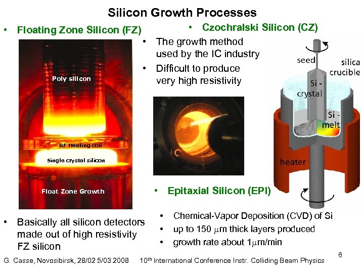 Silicon Growth Processes • Floating Zone Silicon (FZ) Poly silicon • Czochralski Silicon (CZ) • The growth method used by the IC industry • Difficult to produce very high resistivity RF Heating coil Single crystal silicon Czochralski Growth • Epitaxial Silicon (EPI) Float Zone Growth • Basically all silicon detectors made out of high resistivity FZ silicon G. Casse, Novosibirsk, 28/02 5/03 2008 • • • Chemical-Vapor Deposition (CVD) of Si up to 150 m thick layers produced growth rate about 1 m/min 10 th International Conference Instr. Colliding Beam Physics 6
![Silicon Materials under Investigation standard for particle detectors “new” silicon material Thickness [ m] Silicon Materials under Investigation standard for particle detectors “new” silicon material Thickness [ m]](https://present5.com/presentation/fb306b0141b4b0a6b9ba33c1b1764770/image-7.jpg) Silicon Materials under Investigation standard for particle detectors “new” silicon material Thickness [ m] Symbol ( cm) [Oi] (cm-3) Standard FZ (n- and p-type) 50, 100, 150, 300 FZ 1– 30 10 3 < 5 1016 Diffusion oxygenated FZ (n- and ptype) used for LHC Pixel detectors Material 300 DOFZ 1– 7 10 3 ~ 1– 2 1017 Magnetic Czochralski Si, Okmetic, Finland (n- and p-type) 100, 300 MCz ~ 1 10 3 ~ 5 1017 Czochralski Si, Sumitomo, Japan (n-type) 300 Cz ~ 1 10 3 ~ 8 -9 1017 Epitaxial layers on Cz-substrates, ITME, Poland (n- and p-type) 25, 50, 75, 100, 150 EPI 50 – 100 < 1 1017 75 EPI–DO 50 – 100 ~ 7 1017 Diffusion oxyg. Epitaxial layers on CZ • DOFZ silicon • CZ/MCZ silicon • Epi silicon (inhomogeneous) - Enriched with oxygen on wafer level, inhomogeneous distribution of oxygen - high Oi (oxygen) and O 2 i (oxygen dimer) concentration (homogeneous) - formation of shallow Thermal Donors possible - high Oi , O 2 i content due to out-diffusion from the CZ substrate - thin layers: high doping possible (low starting resistivity) • Epi-Do silicon - as EPI, however additional Oi diffused reaching homogeneous Oi content G. Casse, Novosibirsk, 28/02 5/03 2008 10 th International Conference Instr. Colliding Beam Physics 7
Silicon Materials under Investigation standard for particle detectors “new” silicon material Thickness [ m] Symbol ( cm) [Oi] (cm-3) Standard FZ (n- and p-type) 50, 100, 150, 300 FZ 1– 30 10 3 < 5 1016 Diffusion oxygenated FZ (n- and ptype) used for LHC Pixel detectors Material 300 DOFZ 1– 7 10 3 ~ 1– 2 1017 Magnetic Czochralski Si, Okmetic, Finland (n- and p-type) 100, 300 MCz ~ 1 10 3 ~ 5 1017 Czochralski Si, Sumitomo, Japan (n-type) 300 Cz ~ 1 10 3 ~ 8 -9 1017 Epitaxial layers on Cz-substrates, ITME, Poland (n- and p-type) 25, 50, 75, 100, 150 EPI 50 – 100 < 1 1017 75 EPI–DO 50 – 100 ~ 7 1017 Diffusion oxyg. Epitaxial layers on CZ • DOFZ silicon • CZ/MCZ silicon • Epi silicon (inhomogeneous) - Enriched with oxygen on wafer level, inhomogeneous distribution of oxygen - high Oi (oxygen) and O 2 i (oxygen dimer) concentration (homogeneous) - formation of shallow Thermal Donors possible - high Oi , O 2 i content due to out-diffusion from the CZ substrate - thin layers: high doping possible (low starting resistivity) • Epi-Do silicon - as EPI, however additional Oi diffused reaching homogeneous Oi content G. Casse, Novosibirsk, 28/02 5/03 2008 10 th International Conference Instr. Colliding Beam Physics 7
 Irradiation facilities RD 50 institutes enjoy access to several world class irradiation facilities. In particular, the irradiations of the silicon detectors here shown have been performed in the CERN/PS Irrad 1 (maintained by Maurice Glaser) and in the Triga nuclear reactor of the J. Stefan Institute of Ljubljana. Many thanks for the irradiation! G. Casse, Novosibirsk, 28/02 5/03 2008 10 th International Conference Instr. Colliding Beam Physics 8
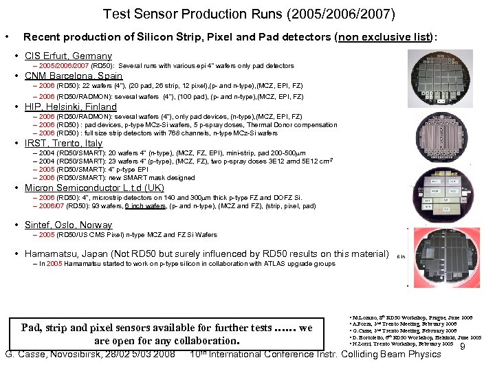 Test Sensor Production Runs (2005/2006/2007) • Recent production of Silicon Strip, Pixel and Pad detectors (non exclusive list): • CIS Erfurt, Germany – 2005/2006/2007 (RD 50): Several runs with various epi 4” wafers only pad detectors • CNM Barcelona, Spain – 2006 (RD 50): 22 wafers (4”), (20 pad, 26 strip, 12 pixel), (p- and n-type), (MCZ, EPI, FZ) – 2006 (RD 50/RADMON): several wafers (4”), (100 pad), (p- and n-type), (MCZ, EPI, FZ) • HIP, Helsinki, Finland – 2006 (RD 50/RADMON): several wafers (4”), only pad devices, (n-type), (MCZ, EPI, FZ) – 2006 (RD 50) : pad devices, p-type MCz-Si wafers, 5 p-spray doses, Thermal Donor compensation – 2006 (RD 50) : full size strip detectors with 768 channels, n-type MCz-Si wafers • IRST, Trento, Italy – – 2004 (RD 50/SMART): 20 wafers 4” (n-type), (MCZ, FZ, EPI), mini-strip, pad 200 -500 m 2004 (RD 50/SMART): 23 wafers 4” (p-type), (MCZ, FZ), two p-spray doses 3 E 12 amd 5 E 12 cm-2 2005 (RD 50/SMART): 4” p-type EPI 2006 (RD 50/SMART): new SMART mask designed • Micron Semiconductor L. t. d (UK) – 2006 (RD 50): 4”, microstrip detectors on 140 and 300 m thick p-type FZ and DOFZ Si. – 2006/07 (RD 50): 93 wafers, 6 inch wafers, (p- and n-type), (MCZ and FZ), (strip, pixel, pad) • Sintef, Oslo, Norway – 2005 (RD 50/US CMS Pixel) n-type MCZ and FZ Si Wafers • Hamamatsu, Japan (Not RD 50 but surely influenced by RD 50 results on this material) – In 2005 Hamamatsu started to work on p-type silicon in collaboration with ATLAS upgrade groups Pad, strip and pixel sensors available for further tests …… we are open for any collaboration. G. Casse, Novosibirsk, 28/02 5/03 2008 • M. Lozano, 8 th RD 50 Workshop, Prague, June 2006 • A. Pozza, 2 nd Trento Meeting, February 2006 • G. Casse, 2 nd Trento Meeting, February 2006 • D. Bortoletto, 6 th RD 50 Workshop, Helsinki, June 2005 • N. Zorzi, Trento Workshop, February 2005 10 th International Conference Instr. Colliding Beam Physics 9
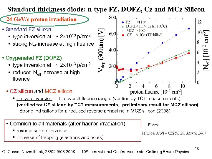 Standard thickness diode: n-type FZ, DOFZ, Cz and MCz Silicon 24 Ge. V/c proton irradiation • Standard FZ silicon • type inversion at ~ 2 1013 p/cm 2 • strong Neff increase at high fluence • Oxygenated FZ (DOFZ) • type inversion at ~ 2 1013 p/cm 2 • reduced Neff increase at high fluence • CZ silicon and MCZ silicon § no type inversion in the overall fluence range (verified by TCT measurements) (verified for CZ silicon by TCT measurements, preliminary result for MCZ silicon) Strong indications for a reduced reverse annealing in MCZ silicon (2006) • Common to all materials (after hadron irradiation): From: § reverse current increase § increase of trapping (electrons and holes) G. Casse, Novosibirsk, 28/02 5/03 2008 10 th International Conference Instr. Colliding Beam Physics 10
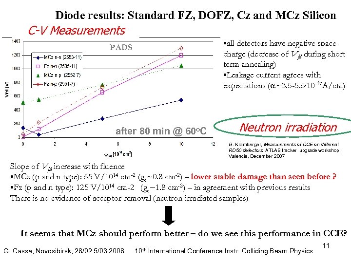 Diode results: Standard FZ, DOFZ, Cz and MCz Silicon C-V Measurements • all detectors have negative space charge (decrease of Vfd during short term annealing) • Leakage current agrees with expectations (a~3. 5 -5. 5∙ 10 -17 A/cm) PADS after 80 min @ 60 o. C Neutron irradiation G. Kramberger, Measurements of CCE on different RD 50 detectors, ATLAS tracker upgrade workshop, Valencia, December 2007 Slope of Vfd increase with fluence • MCz (p and n type): 55 V/1014 cm-2 (gc~0. 8 cm-2) – lower stable damage than seen before ? • Fz (p and n type): 125 V/1014 cm-2 (gc~1. 8 cm-2) – in agreement with previous results There is no evidence of acceptor removal (neutron irradiated samples) It seems that MCz should perform better – do we see this performance in CCE? G. Casse, Novosibirsk, 28/02 5/03 2008 10 th International Conference Instr. Colliding Beam Physics 11
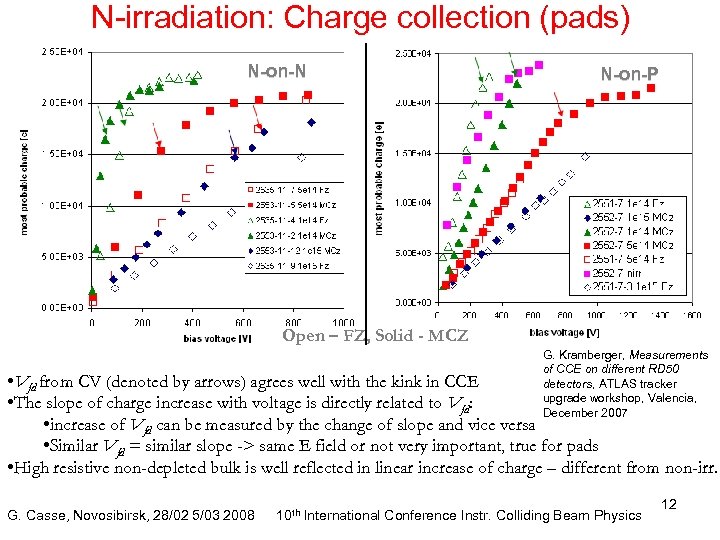 N-irradiation: Charge collection (pads) N-on-N N-on-P Open – FZ, Solid - MCZ G. Kramberger, Measurements of CCE on different RD 50 detectors, ATLAS tracker upgrade workshop, Valencia, December 2007 • Vfd from CV (denoted by arrows) agrees well with the kink in CCE • The slope of charge increase with voltage is directly related to Vfd: • increase of Vfd can be measured by the change of slope and vice versa • Similar Vfd = similar slope -> same E field or not very important, true for pads • High resistive non-depleted bulk is well reflected in linear increase of charge – different from non-irr. G. Casse, Novosibirsk, 28/02 5/03 2008 10 th International Conference Instr. Colliding Beam Physics 12
 Diode results: thin FZ detectors and epitaxial Si Ø Why thin detectors? Advantage: lower depletion voltage (Vfd d 2), full depletion at large possible lower leakage current (? ? ) (Irev d): if yes lower noise contribution, lower power dissipation smaller collection time (tc d), less charge carrier trapping Draw back: smaller signal for mips (signal d) larger capacitance (Cdet 1/d), larger electronic noise find an optimal thickness Ø Questions: Motivation - depend the damage effects on the device thickness? - which impurities play a major role in the damage (P, O, C, H, others)? E. Fretwurst et al. , 11 th RD 50 workshop G. Casse, Novosibirsk, 28/02 5/03 2008 10 th International Conference Instr. Colliding Beam Physics 13
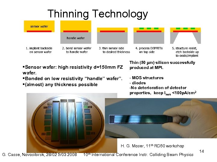 Thinning Technology §Sensor wafer: high resistivity d=150 mm FZ wafer. §Bonded on low resistivity “handle” wafer”. §(almost) any thickness possible Thin (50 mm) silicon successfully produced at MPI. - MOS structures - diodes -No deterioration of detector properties, keep Ileak <100 p. A/cm 2 H. G. Moser, 11 th RD 50 workshop G. Casse, Novosibirsk, 28/02 5/03 2008 10 th International Conference Instr. Colliding Beam Physics 14
![Oxygen depth profiles § EPI-ST, 72 µm: [O] inhomogeneous, <[O]> = 9. 3 1016 Oxygen depth profiles § EPI-ST, 72 µm: [O] inhomogeneous, <[O]> = 9. 3 1016](https://present5.com/presentation/fb306b0141b4b0a6b9ba33c1b1764770/image-15.jpg) Oxygen depth profiles § EPI-ST, 72 µm: [O] inhomogeneous, <[O]> = 9. 3 1016 cm-3 § EPI-DO, 72 µm: [O] homogeneous, except surface, <[O]> = 6. 0 1017 cm-3 § MCz: [O] homogeneous, except surface <[O]> = 5. 2 1017 cm-3 E. Fretwurst et al. , 11 th RD 50 workshop G. Casse, Novosibirsk, 28/02 5/03 2008 § EPI-ST, 100/150 µm: [O] inhomogeneous, <[O]> = 5. 4 1016 / 4. 5 1016 cm-3 § EPI-DO, 100/150 µm: [O] more homogeneous, <[O]> = 2. 8 1017 / 1. 4 1017 cm-3 § FZ 50 µm: inhomogeneous <[O]> = 3. 0 1016 cm-3 § FZ 100 µm: homogeneous, except surface <[O]> = 1. 4 1016 cm-3 10 th International Conference Instr. Colliding Beam Physics 15
Oxygen depth profiles § EPI-ST, 72 µm: [O] inhomogeneous, <[O]> = 9. 3 1016 cm-3 § EPI-DO, 72 µm: [O] homogeneous, except surface, <[O]> = 6. 0 1017 cm-3 § MCz: [O] homogeneous, except surface <[O]> = 5. 2 1017 cm-3 E. Fretwurst et al. , 11 th RD 50 workshop G. Casse, Novosibirsk, 28/02 5/03 2008 § EPI-ST, 100/150 µm: [O] inhomogeneous, <[O]> = 5. 4 1016 / 4. 5 1016 cm-3 § EPI-DO, 100/150 µm: [O] more homogeneous, <[O]> = 2. 8 1017 / 1. 4 1017 cm-3 § FZ 50 µm: inhomogeneous <[O]> = 3. 0 1016 cm-3 § FZ 100 µm: homogeneous, except surface <[O]> = 1. 4 1016 cm-3 10 th International Conference Instr. Colliding Beam Physics 15
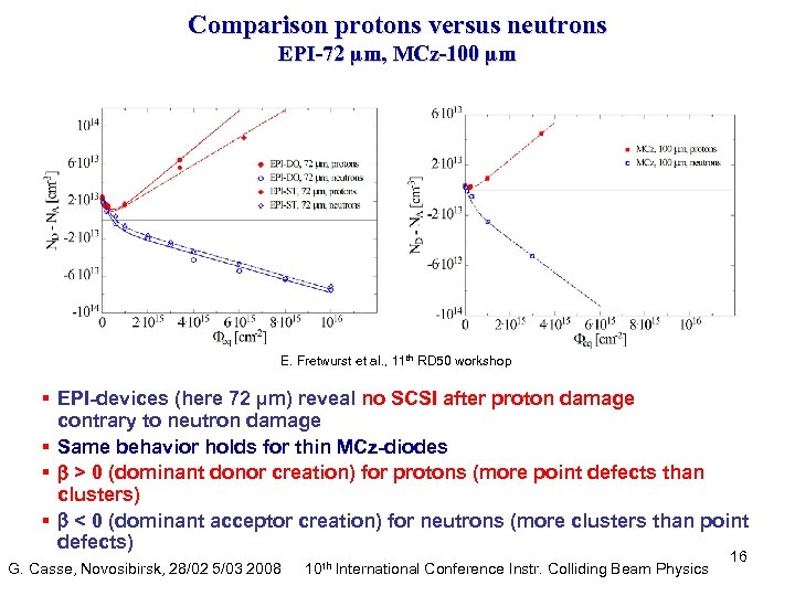 Comparison protons versus neutrons EPI-72 µm, MCz-100 µm E. Fretwurst et al. , 11 th RD 50 workshop § EPI-devices (here 72 µm) reveal no SCSI after proton damage contrary to neutron damage § Same behavior holds for thin MCz-diodes § > 0 (dominant donor creation) for protons (more point defects than clusters) § < 0 (dominant acceptor creation) for neutrons (more clusters than point defects) G. Casse, Novosibirsk, 28/02 5/03 2008 10 th International Conference Instr. Colliding Beam Physics 16
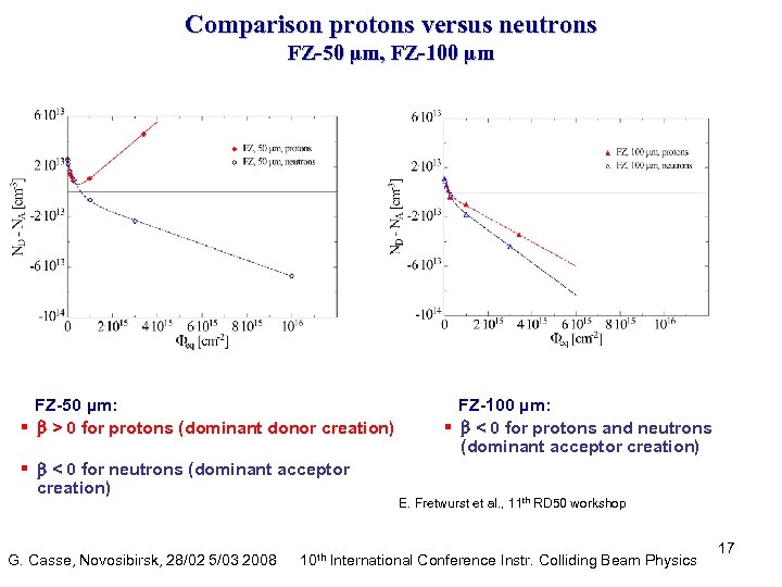 Comparison protons versus neutrons FZ-50 µm, FZ-100 µm FZ-50 µm: § > 0 for protons (dominant donor creation) § < 0 for neutrons (dominant acceptor creation) G. Casse, Novosibirsk, 28/02 5/03 2008 FZ-100 µm: § < 0 for protons and neutrons (dominant acceptor creation) E. Fretwurst et al. , 11 th RD 50 workshop 10 th International Conference Instr. Colliding Beam Physics 17
 Possible advantages of non -inverted detectors: reverse-annealing E. Fretwurst et al. , 11 th RD 50 workshop G. Casse, Novosibirsk, 28/02 5/03 2008 10 th International Conference Instr. Colliding Beam Physics 18
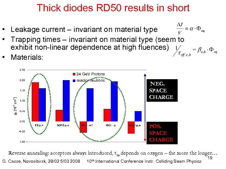 Thick diodes RD 50 results in short • Leakage current – invariant on material type • Trapping times – invariant on material type (seem to exhibit non-linear dependence at high fluences) • Materials: NEG. SPACE CHARGE POS. SPACE CHARGE Reverse annealing: acceptors always introduced, tra depends on oxygen – the more the longer… G. Casse, Novosibirsk, 28/02 5/03 2008 10 th International Conference Instr. Colliding Beam Physics 19
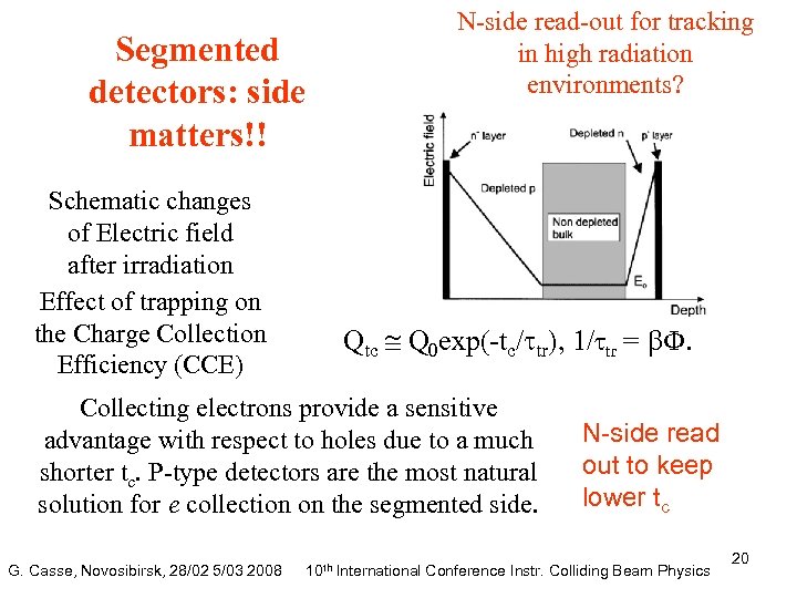 Segmented detectors: side matters!! Schematic changes of Electric field after irradiation Effect of trapping on the Charge Collection Efficiency (CCE) N-side read-out for tracking in high radiation environments? Qtc Q 0 exp(-tc/ttr), 1/ttr = b. Collecting electrons provide a sensitive advantage with respect to holes due to a much shorter tc. P-type detectors are the most natural solution for e collection on the segmented side. G. Casse, Novosibirsk, 28/02 5/03 2008 N-side read out to keep lower tc 10 th International Conference Instr. Colliding Beam Physics 20
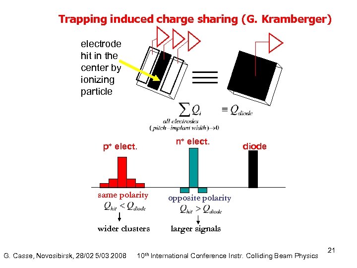 Trapping induced charge sharing (G. Kramberger) electrode hit in the center by ionizing particle p+ elect. same polarity wider clusters G. Casse, Novosibirsk, 28/02 5/03 2008 n+ elect. diode opposite polarity larger signals 10 th International Conference Instr. Colliding Beam Physics 21
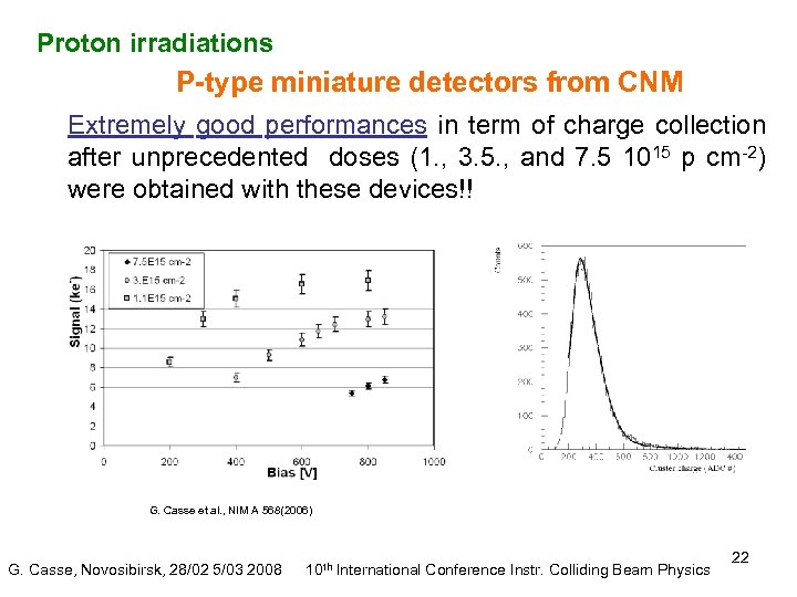 Proton irradiations P-type miniature detectors from CNM Extremely good performances in term of charge collection after unprecedented doses (1. , 3. 5. , and 7. 5 1015 p cm-2) were obtained with these devices!! G. Casse et al. , NIM A 568(2006) G. Casse, Novosibirsk, 28/02 5/03 2008 10 th International Conference Instr. Colliding Beam Physics 22
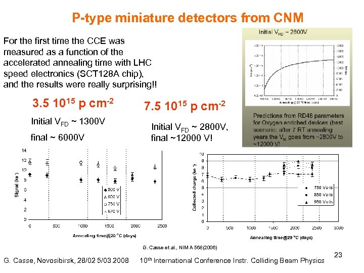 P-type miniature detectors from CNM For the first time the CCE was measured as a function of the accelerated annealing time with LHC speed electronics (SCT 128 A chip), and the results were really surprising!! 3. 5 1015 p cm-2 Initial VFD ~ 1300 V final ~ 6000 V 7. 5 1015 p cm-2 Initial VFD ~ 2800 V, final ~12000 V! G. Casse et al. , NIM A 568(2006) G. Casse, Novosibirsk, 28/02 5/03 2008 10 th International Conference Instr. Colliding Beam Physics 23
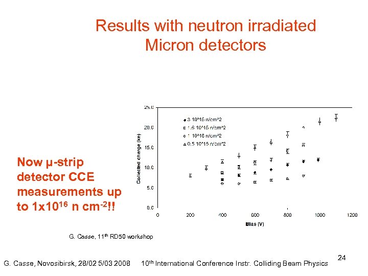 Results with neutron irradiated Micron detectors Now µ-strip detector CCE measurements up to 1 x 10¹⁶ n cm-2!! G. Casse, 11 th RD 50 workshop G. Casse, Novosibirsk, 28/02 5/03 2008 10 th International Conference Instr. Colliding Beam Physics 24
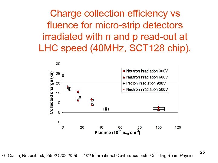 Charge collection efficiency vs fluence for micro-strip detectors irradiated with n and p read-out at LHC speed (40 MHz, SCT 128 chip). G. Casse, Novosibirsk, 28/02 5/03 2008 10 th International Conference Instr. Colliding Beam Physics 25
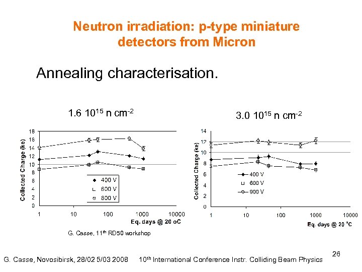 Neutron irradiation: p-type miniature detectors from Micron Annealing characterisation. 1. 6 1015 n cm-2 3. 0 1015 n cm-2 G. Casse, 11 th RD 50 workshop G. Casse, Novosibirsk, 28/02 5/03 2008 10 th International Conference Instr. Colliding Beam Physics 26
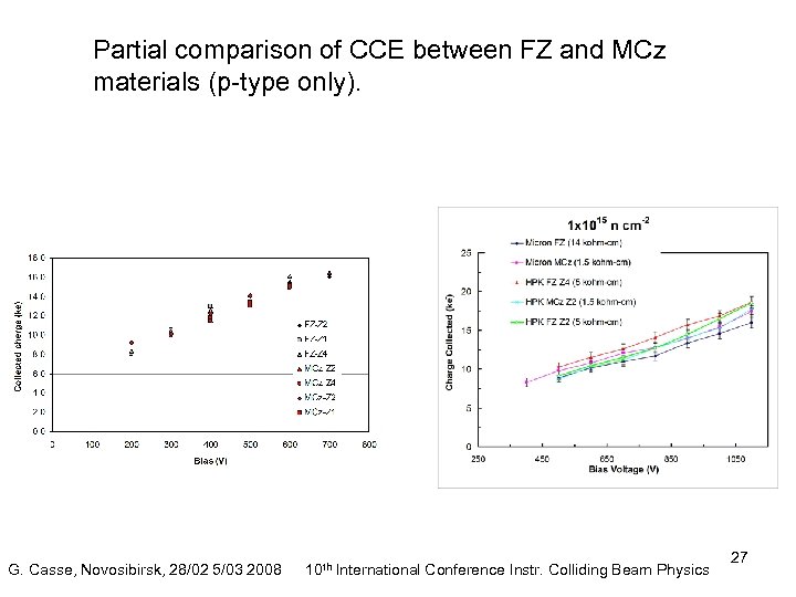 Partial comparison of CCE between FZ and MCz materials (p-type only). G. Casse, Novosibirsk, 28/02 5/03 2008 10 th International Conference Instr. Colliding Beam Physics 27
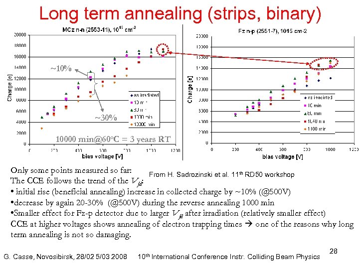 Long term annealing (strips, binary) ~10% ~30% 10000 min@60 o. C = 3 years RT Only some points measured so far: From H. Sadrozinski et al. 11 th RD 50 workshop The CCE follows the trend of the Vfd: • initial rise (beneficial annealing) increase in collected charge by ~10% (@500 V) • decrease by again 20 -30% (@500 V) during the reverse annealing 1000 min • Smaller effect for Fz-p detector due to larger Vfd after irradiation (relatively smaller effect) CCE at higher voltages shows annealing of electron trapping times one of the reasons why long term annealing is not so damaging. G. Casse, Novosibirsk, 28/02 5/03 2008 10 th International Conference Instr. Colliding Beam Physics 28
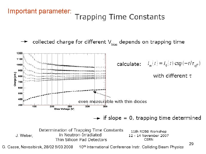 Important parameter: J. Weber, G. Casse, Novosibirsk, 28/02 5/03 2008 10 th International Conference Instr. Colliding Beam Physics 29
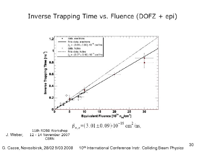 J. Weber, G. Casse, Novosibirsk, 28/02 5/03 2008 10 th International Conference Instr. Colliding Beam Physics 30
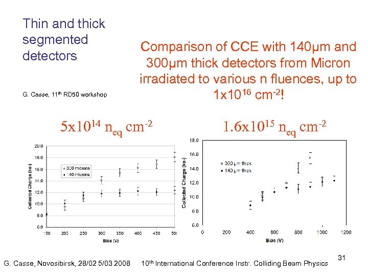 Thin and thick segmented detectors G. Casse, 11 th RD 50 workshop Comparison of CCE with 140µm and 300µm thick detectors from Micron irradiated to various n fluences, up to 1 x 1016 cm-2! 5 x 10¹⁴ neq cm-2 G. Casse, Novosibirsk, 28/02 5/03 2008 1. 6 x 10¹⁵ neq cm-2 10 th International Conference Instr. Colliding Beam Physics 31
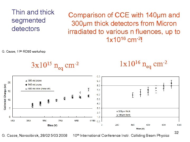 Thin and thick segmented detectors Comparison of CCE with 140µm and 300µm thick detectors from Micron irradiated to various n fluences, up to 1 x 1016 cm-2! G. Casse, 11 th RD 50 workshop 3 x 10¹⁵ neq cm-2 G. Casse, Novosibirsk, 28/02 5/03 2008 1 x 10¹⁶ neq cm-2 10 th International Conference Instr. Colliding Beam Physics 32
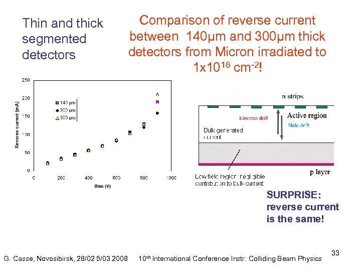 Thin and thick segmented detectors Comparison of reverse current between 140µm and 300µm thick detectors from Micron irradiated to 1 x 1016 cm-2! SURPRISE: reverse current is the same! G. Casse, Novosibirsk, 28/02 5/03 2008 10 th International Conference Instr. Colliding Beam Physics 33
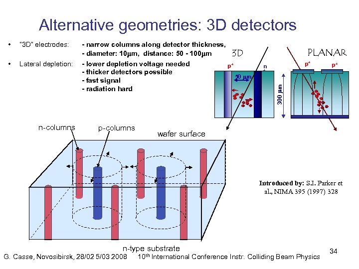 Alternative geometries: 3 D detectors “ 3 D” electrodes: • Lateral depletion: - narrow columns along detector thickness, - diameter: 10 mm, distance: 50 - 100 mm 3 D - lower depletion voltage needed p+ - thicker detectors possible 50 mm - fast signal - radiation hard -- ++ + n-columns p-columns PLANAR p+ n p+ + 300 mm • - ++ + wafer surface Introduced by: S. I. Parker et al. , NIMA 395 (1997) 328 n-type substrate G. Casse, Novosibirsk, 28/02 5/03 2008 10 th International Conference Instr. Colliding Beam Physics 34
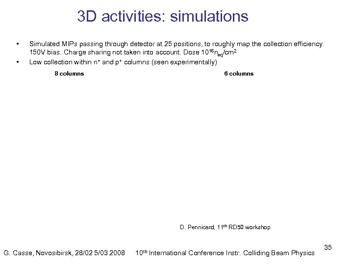 3 D activities: simulations • • Simulated MIPs passing through detector at 25 positions, to roughly map the collection efficiency. 150 V bias. Charge sharing not taken into account. Dose 1016 neq/cm 2 Low collection within n+ and p+ columns (seen experimentally) 8 columns 6 columns D. Pennicard, 11 th RD 50 workshop G. Casse, Novosibirsk, 28/02 5/03 2008 10 th International Conference Instr. Colliding Beam Physics 35
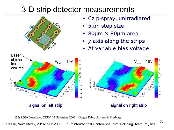 3 -D strip detector measurements G. Casse, Novosibirsk, 28/02 5/03 2008 10 th International Conference Instr. Colliding Beam Physics 36
 OUTLOOK: Investigation of n-MCz detectors with proton irradiation Further Investigation of O and thickness effects Systematic investigation of the effect of initial wafer resistivity Investigate best solution for interstrip isolation Investigation of optimal solution for diode geometry in 3 D devices. Quest for satisfactory microscopy model with accurate prediction of the electrical properties of the devices G. Casse, Novosibirsk, 28/02 5/03 2008 10 th International Conference Instr. Colliding Beam Physics 37
 SPARES G. Casse, Novosibirsk, 28/02 5/03 2008 10 th International Conference Instr. Colliding Beam Physics 38
 EPI Devices – Irradiation experiments • G. Lindström et al. , 10 th European Symposium on Semiconductor Detectors, 12 -16 June 2005 Epitaxial silicon G. Kramberger et al. , Hamburg RD 50 Workshop, August 2006 – Layer thickness: 25, 50, 75 m (resistivity: ~ 50 cm); 150 m (resistivity: ~ 400 cm) – Oxygen: [O] 9 1016 cm-3; Oxygen dimers (detected via IO 2 -defect formation) 105 V (25 mm) 230 V (50 mm) 320 V (75 mm) – Only little change in depletion voltage – No type inversion up to ~ 1016 p/cm 2 and ~ 1016 n/cm 2 high electric field will stay at front electrode! – CCE (Sr 90 source, 25 ns shaping): 6400 e (150 m; 2 x 10¹⁵ n/cm-2) 3300 e (75 m; 8 x 10¹⁵ n/cm-2) 2300 e (50 m; 8 x 10¹⁵ n/cm-2) – Explanation: introduction of shallow donors is bigger than generation of deep acceptors G. Casse, Novosibirsk, 28/02 5/03 2008 10 th International Conference Instr. Colliding Beam Physics 39
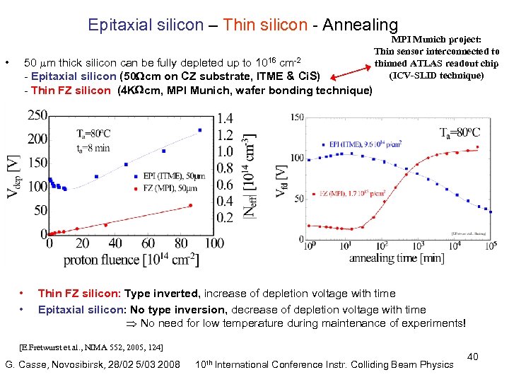 Epitaxial silicon – Thin silicon - Annealing 50 m thick silicon can be fully depleted up to 1016 cm-2 - Epitaxial silicon (50 cm on CZ substrate, ITME & Ci. S) - Thin FZ silicon (4 K cm, MPI Munich, wafer bonding technique) • • • MPI Munich project: Thin sensor interconnected to thinned ATLAS readout chip (ICV-SLID technique) Thin FZ silicon: Type inverted, increase of depletion voltage with time Epitaxial silicon: No type inversion, decrease of depletion voltage with time No need for low temperature during maintenance of experiments! [E. Fretwurst et al. , NIMA 552, 2005, 124] G. Casse, Novosibirsk, 28/02 5/03 2008 10 th International Conference Instr. Colliding Beam Physics 40
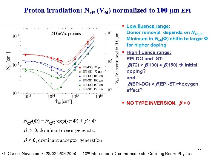 Proton irradiation: Neff (Vfd) normalized to 100 µm EPI § Low fluence range: Donor removal, depends on Neff, 0, Minimum in Neff( ) shifts to larger for higher doping § High fluence range: EPI-DO and -ST: (72) > (100) (150) initial doping? and (EPI-DO) > (EPI-ST) oxygen effect? § NO TYPE INVERSION, > 0 Neff ( ) = Neff, 0·exp(-c· ) + · > 0, dominant donor generation < 0, dominant acceptor generation G. Casse, Novosibirsk, 28/02 5/03 2008 10 th International Conference Instr. Colliding Beam Physics 41
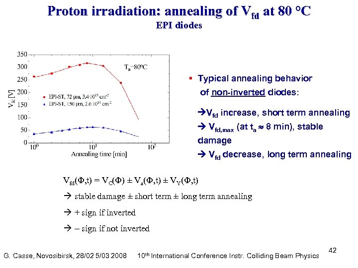 Proton irradiation: annealing of Vfd at 80 °C EPI diodes § Typical annealing behavior of non-inverted diodes: Vfd increase, short term annealing Vfd, max (at ta 8 min), stable damage Vfd decrease, long term annealing Vfd( , t) = VC( ) ± Va( , t) ± VY( , t) stable damage ± short term ± long term annealing + sign if inverted sign if not inverted G. Casse, Novosibirsk, 28/02 5/03 2008 10 th International Conference Instr. Colliding Beam Physics 42
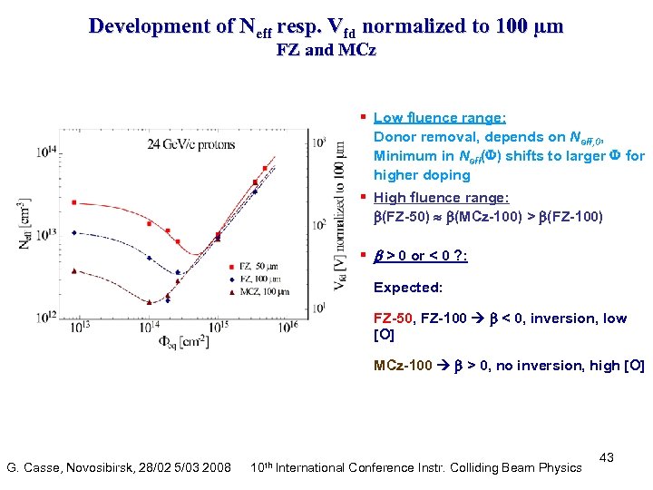 Development of Neff resp. Vfd normalized to 100 µm FZ and MCz § Low fluence range: Donor removal, depends on Neff, 0, Minimum in Neff( ) shifts to larger for higher doping § High fluence range: (FZ-50) (MCz-100) > (FZ-100) § > 0 or < 0 ? : Expected: FZ-50, FZ-100 < 0, inversion, low [O] MCz-100 > 0, no inversion, high [O] G. Casse, Novosibirsk, 28/02 5/03 2008 10 th International Conference Instr. Colliding Beam Physics 43
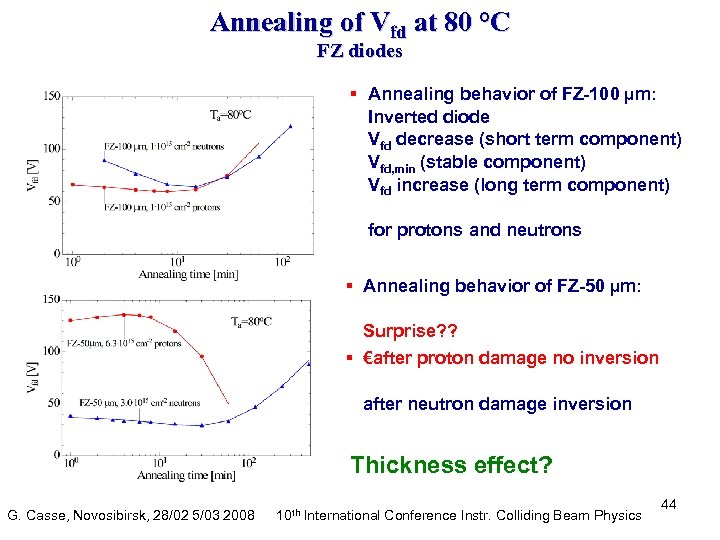 Annealing of Vfd at 80 °C FZ diodes § Annealing behavior of FZ-100 µm: Inverted diode Vfd decrease (short term component) Vfd, min (stable component) Vfd increase (long term component) for protons and neutrons § Annealing behavior of FZ-50 µm: Surprise? ? § €after proton damage no inversion after neutron damage inversion Thickness effect? G. Casse, Novosibirsk, 28/02 5/03 2008 10 th International Conference Instr. Colliding Beam Physics 44


