c315e0527fb70dbc477771d317466c9d.ppt
- Количество слайдов: 51
 Overview n n History of silicon for tracking detectors & Basics From LHC tracker to SLHC tracker Radiation effects in silicon - defect engineering Device engineering – radiation hard device design n Silicon detectors for SLHC n n n+-p strip detectors n+-p pixel detectors 3 D detectors Electronics considerations Conclusions DESY seminar 9. 1. 2007 Signal formation Isolation techniques G. Kramberger, Jožef Stefan Institute, Towards Radiation Hard Silicon Detectros at SLHC 1
 History and basics DESY seminar 9. 1. 2007 G. Kramberger, Jožef Stefan Institute, Towards Radiation Hard Silicon Detectros at SLHC 2
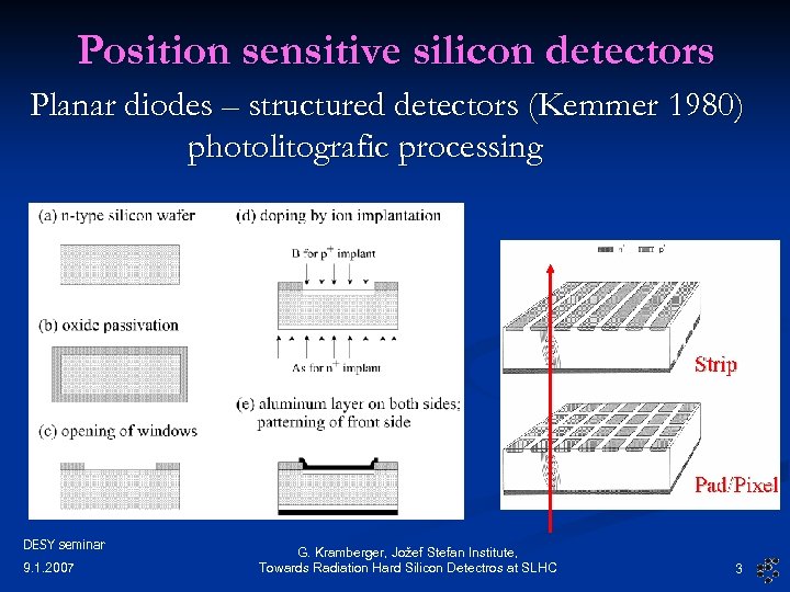 Position sensitive silicon detectors Planar diodes – structured detectors (Kemmer 1980) photolitografic processing DESY seminar 9. 1. 2007 G. Kramberger, Jožef Stefan Institute, Towards Radiation Hard Silicon Detectros at SLHC 3
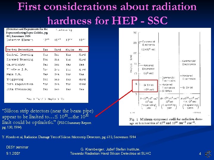 First considerations about radiation hardness for HEP - SSC (Detectors and Experiments for the Superconducting Super Collider, pg. 491, Snowmass 1984 considerations for SSC (Detectors and Experiments for the Superconducting Super Collider, pg. 491, Snowmass 1984 Now 105 upra “Silicon strip detectors (near the beam pipe) appear to be limited to…≤ 1032. . the 1032 limit could be optimistic. ” (PSSC Summary Report pg. 130, 1984) T. Kondo et al, Radiation Damage Test of Silicon Microstrip Detectors, pg. 612, Snowmass 1984 DESY seminar 9. 1. 2007 G. Kramberger, Jožef Stefan Institute, Towards Radiation Hard Silicon Detectros at SLHC 4
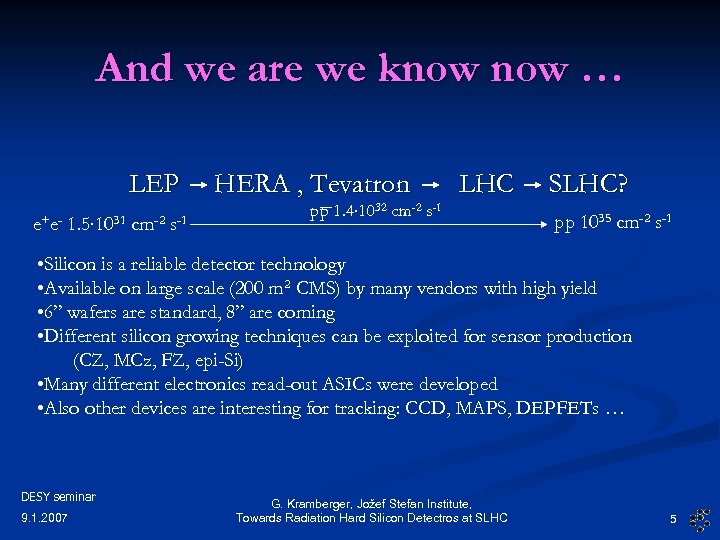 And we are we know … LEP e+e- 1. 5∙ 1031 cm-2 s-1 HERA , Tevatron LHC pp 1. 4∙ 1032 cm-2 s-1 SLHC? pp 1035 cm-2 s-1 • Silicon is a reliable detector technology • Available on large scale (200 m 2 CMS) by many vendors with high yield • 6’’ wafers are standard, 8’’ are coming • Different silicon growing techniques can be exploited for sensor production (CZ, MCz, FZ, epi-Si) • Many different electronics read-out ASICs were developed • Also other devices are interesting for tracking: CCD, MAPS, DEPFETs … DESY seminar 9. 1. 2007 G. Kramberger, Jožef Stefan Institute, Towards Radiation Hard Silicon Detectros at SLHC 5
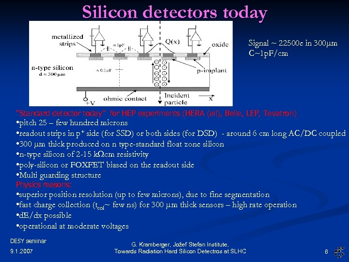 Silicon detectors today Signal ~ 22500 e in 300 mm C~1 p. F/cm “Standard detector today” for HEP experiments (HERA (all), Belle, LEP, Tevatron) • pitch 25 – few hundred microns • readout strips in p+ side (for SSD) or both sides (for DSD) - around 6 cm long AC/DC coupled • 300 mm thick produced on n type-standard float zone silicon • n-type silicon of 2 -15 k. Wcm resistivity • poly-silicon or FOXFET biased on the readout side • Multi guarding structure Physics reasons: • superior position resolution (up to few microns), due to fine segmentation • fast charge collection (tcol~ few ns) for 300 mm thick sensors – high rate operation • d. E/dx possible • operational at moderate voltages DESY seminar 9. 1. 2007 G. Kramberger, Jožef Stefan Institute, Towards Radiation Hard Silicon Detectros at SLHC 6
 LHC & SLHC DESY seminar 9. 1. 2007 G. Kramberger, Jožef Stefan Institute, Towards Radiation Hard Silicon Detectros at SLHC 7
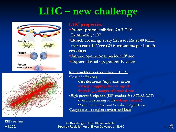 LHC – new challenge LHC properties §Proton-proton collider, 2 x 7 Te. V Luminosity: 1034 §Bunch crossing: every 25 nsec, Rate: 40 MHz event rate: 109/sec (23 interactions per bunch crossing) §Annual operational period: 107 sec §Expected total op. period: 10 years Main problems of a tracker at LHC: • Loss of efficiency • fast electronics (high series noise) • charge trapping (loss of signal) • high Ubias , danger of break-down • High power dissipation (8 W/module for ATLAS-SCT) • Need for running cool (leakage current) • Need for storing cool to reduce Vfd increase • Large scale – complex services and links DESY seminar 9. 1. 2007 G. Kramberger, Jožef Stefan Institute, Towards Radiation Hard Silicon Detectros at SLHC 8
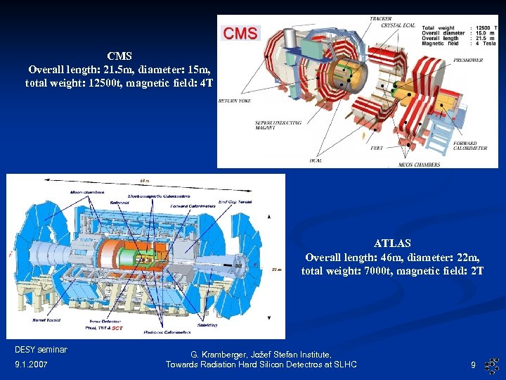 CMS Overall length: 21. 5 m, diameter: 15 m, total weight: 12500 t, magnetic field: 4 T ATLAS Overall length: 46 m, diameter: 22 m, total weight: 7000 t, magnetic field: 2 T DESY seminar 9. 1. 2007 G. Kramberger, Jožef Stefan Institute, Towards Radiation Hard Silicon Detectros at SLHC 9
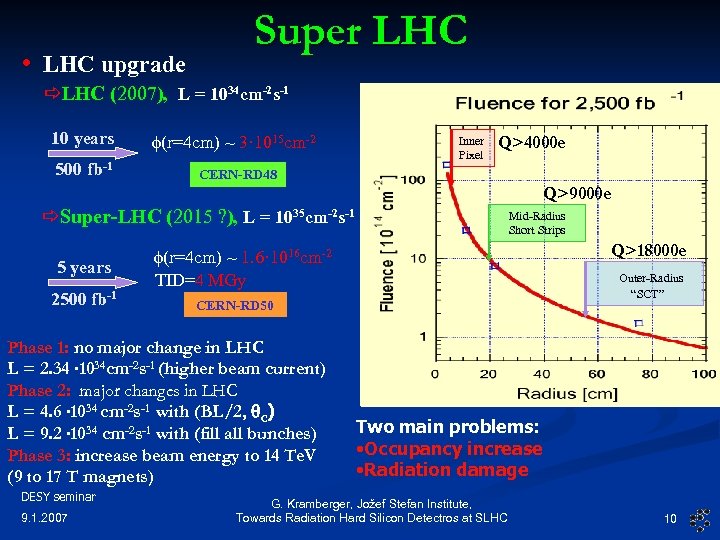 Super LHC • LHC upgrade LHC (2007), L = 1034 cm-2 s-1 f(r=4 cm) 10 years 500 fb-1 ~ 3· 1015 cm-2 Inner Pixel Q>4000 e ~5000 e CERN-RD 48 Super-LHC (2015 ? ), L = 1035 cm-2 s-1 Q>9000 e Mid-Radius Short Strips Q>18000 e f(r=4 cm) 5 years 2500 fb-1 ~ 1. 6· 1016 cm-2 TID=4 MGy CERN-RD 50 Phase 1: no major change in LHC L = 2. 34 ∙ 1034 cm-2 s-1 (higher beam current) Phase 2: major changes in LHC L = 4. 6 ∙ 1034 cm-2 s-1 with (BL/2, qc) L = 9. 2 ∙ 1034 cm-2 s-1 with (fill all bunches) Phase 3: increase beam energy to 14 Te. V (9 to 17 T magnets) DESY seminar 9. 1. 2007 Outer-Radius “SCT” Two main problems: • Occupancy increase • Radiation damage G. Kramberger, Jožef Stefan Institute, Towards Radiation Hard Silicon Detectros at SLHC 10
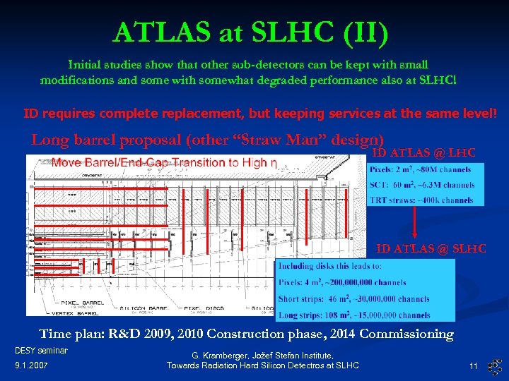 ATLAS at SLHC (II) Initial studies show that other sub-detectors can be kept with small modifications and some with somewhat degraded performance also at SLHC! ID requires complete replacement, but keeping services at the same level! Long barrel proposal (other “Straw Man” design) ID ATLAS @ LHC ID ATLAS @ SLHC Time plan: R&D 2009, 2010 Construction phase, 2014 Commissioning DESY seminar 9. 1. 2007 G. Kramberger, Jožef Stefan Institute, Towards Radiation Hard Silicon Detectros at SLHC 11
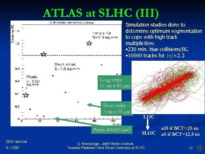 ATLAS at SLHC (III) Simulation studies done to determine optimum segmentation to cope with high track multiplicities: • 230 min. bias collisions/BC • 10000 tracks for |h|<2. 3 Long strips 12 cm x 80 mm Short strips 3 cm x 50 mm Pixels 400 x 50 mm 2 DESY seminar 9. 1. 2007 LHC SLHC G. Kramberger, Jožef Stefan Institute, Towards Radiation Hard Silicon Detectros at SLHC x 10 if BCT=25 ns x 5 if BCT=12. 5 ns 12
 Radiation damage in semiconductor detectors DESY seminar 9. 1. 2007 G. Kramberger, Jožef Stefan Institute, Towards Radiation Hard Silicon Detectros at SLHC 13
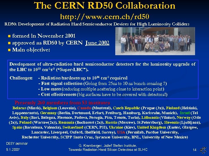 The CERN RD 50 Collaboration http: //www. cern. ch/rd 50 RD 50: Development of Radiation Hard Semiconductor Devices for High Luminosity Colliders n formed in November 2001 n approved as RD 50 by CERN June 2002 n Main objective: Development of ultra-radiation hard semiconductor detectors for the luminosity upgrade of the LHC to 1035 cm-2 s-1 (“Super-LHC”). Challenges: - Radiation hardness up to 1016 cm-2 required - Fast signal collection (Going from 25 ns to 10 ns bunch crossing ? ) - Low mass (reducing multiple scattering close to interaction point) - Cost effectiveness (big surfaces have to be covered with detectors!) Presently 260 members from 53 institutes Belarus (Minsk), Belgium (Louvain), Canada (Montreal), Czech Republic (Prague (3 x)), Finland (Helsinki, Lappeenranta), Germany (Berlin, Dortmund, Erfurt, Freiburg, Hamburg, Karlsruhe, Munich), Israel (Tel Aviv), Italy (Bari, Bologna, Florence, Padova, Perugia, Pisa, Trento, Turin), Lithuania (Vilnius), Norway (Oslo (2 x)), Poland (Warsaw(2 x)), Romania (Bucharest (2 x)), Russia (Moscow), St. Petersburg), Slovenia (Ljubljana), Spain (Barcelona, Valencia), Switzerland (CERN, PSI), Ukraine (Kiev), United Kingdom (Exeter, Glasgow, Lancaster, Liverpool, Oxford, Sheffield, Surrey), USA (Fermilab, Purdue University, Rochester University, SCIPP Santa Cruz, Syracuse University, BNL, University of New Mexico) DESY seminar 9. 1. 2007 G. Kramberger, Jožef Stefan Institute, Towards Radiation Hard Silicon Detectros at SLHC 14
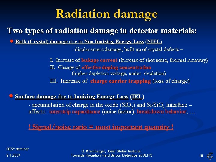 Radiation damage Two types of radiation damage in detector materials: Bulk (Crystal) damage due to Non Ionizing Energy Loss (NIEL) - displacement damage, built up of crystal defects – I. Increase of leakage current (increase of shot noise, thermal runaway) II. Change of effective doping concentration (higher depletion voltage, under- depletion) III. Increase of charge carrier trapping (loss of charge) Surface damage due to Ionizing Energy Loss (IEL) - accumulation of charge in the oxide (Si. O 2) and Si/Si. O 2 interface – affects: interstrip capacitance (noise factor), breakdown behavior, … ! Signal/noise ratio = most important quantity ! DESY seminar 9. 1. 2007 G. Kramberger, Jožef Stefan Institute, Towards Radiation Hard Silicon Detectros at SLHC 15
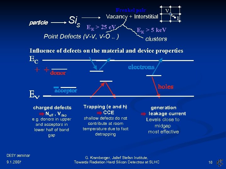 particle Sis Frenkel pair Vacancy + Interstitial EK > 25 e. V Point Defects (V-V, V-O. . ) V I EK > 5 ke. V clusters Influence of defects on the material and device properties charged defects Neff , Vdep e. g. donors in upper and acceptors in lower half of band gap DESY seminar 9. 1. 2007 Trapping (e and h) CCE shallow defects do not contribute at room temperature due to fast detrapping generation leakage current Levels close to midgap most effective G. Kramberger, Jožef Stefan Institute, Towards Radiation Hard Silicon Detectros at SLHC 16
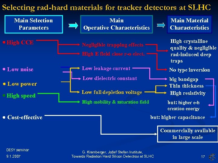 Selecting rad-hard materials for tracker detectors at SLHC Main Selection Parameters High CCE Main Operative Characteristics Main Material Characteristics High crystalline quality & negligible rad-induced deep traps Negligible trapping effects High E field close r-o elect. Low power Low leakage current No type inversion Low dielectric constant Low full depletion voltage big bandgap Thin thickness High resistivity High mobility & saturation field Low noise but: higher e-h High speed creation energy Cost-effective but: higher capacitance Commercially available in large scale DESY seminar 9. 1. 2007 G. Kramberger, Jožef Stefan Institute, Towards Radiation Hard Silicon Detectros at SLHC 17
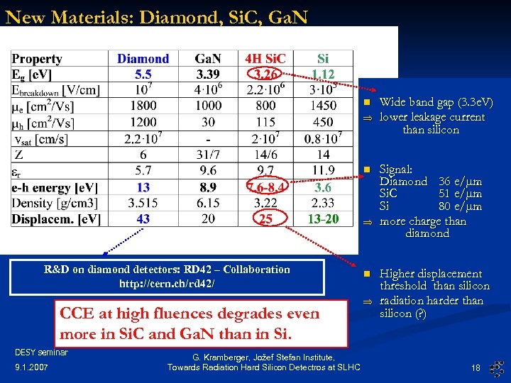 New Materials: Diamond, Si. C, Ga. N n n R&D on diamond detectors: RD 42 – Collaboration http: //cern. ch/rd 42/ CCE at high fluences degrades even more in Si. C and Ga. N than in Si. DESY seminar 9. 1. 2007 G. Kramberger, Jožef Stefan Institute, Towards Radiation Hard Silicon Detectros at SLHC n Wide band gap (3. 3 e. V) lower leakage current than silicon Signal: Diamond 36 e/mm Si. C 51 e/mm Si 80 e/mm more charge than diamond Higher displacement threshold than silicon radiation harder than silicon (? ) 18
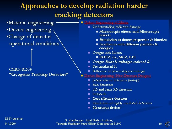 Approaches to develop radiation harder tracking detectors • Material engineering • Device engineering • Change of detector operational conditions CERN RD 39 “Cryogenic Tracking Detectors” DESY seminar 9. 1. 2007 n n Defect Engineering of Silicon n Understanding radiation damage n Macroscopic effects and Microscopic defects n Simulation of defect properties & kinetics n Irradiation with different particles & energies n Oxygen rich Silicon n DOFZ, Cz, MCZ, EPI n Oxygen dimer & hydrogen enriched Si n Pre-irradiated Si n Influence of processing technology Device Engineering (New Detector Designs) n p-type silicon detectors (n-in-p) n thin detectors n 3 D and Semi 3 D detectors n Stripixels n Cost effective detectors n Simulation of highly irradiated detectors n Monolithic devices G. Kramberger, Jožef Stefan Institute, Towards Radiation Hard Silicon Detectros at SLHC 19
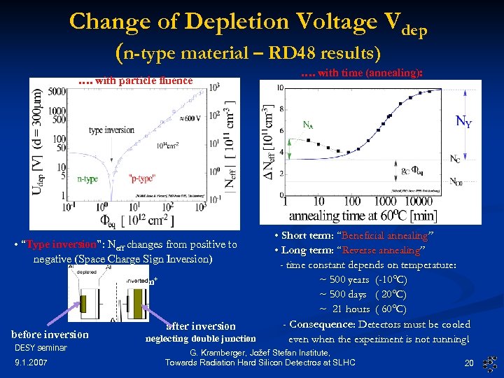 Change of Depletion Voltage Vdep (n-type material – RD 48 results) …. with particle fluence • “Type inversion”: Neff changes from positive to negative (Space Charge Sign Inversion) p+ before inversion DESY seminar 9. 1. 2007 n+ p+ n+ after inversion neglecting double junction …. with time (annealing): • Short term: “Beneficial annealing” • Long term: “Reverse annealing” - time constant depends on temperature: ~ 500 years (-10°C) ~ 500 days ( 20°C) ~ 21 hours ( 60°C) - Consequence: Detectors must be cooled even when the experiment is not running! G. Kramberger, Jožef Stefan Institute, Towards Radiation Hard Silicon Detectros at SLHC 20
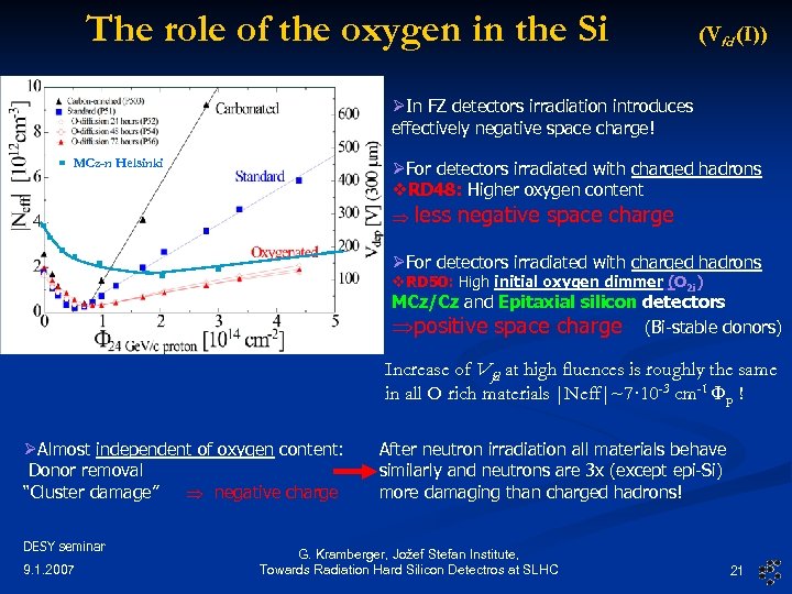 The role of the oxygen in the Si (Vfd (I)) ØIn FZ detectors irradiation introduces effectively negative space charge! MCz-n Helsinki ØFor detectors irradiated with charged hadrons v. RD 48: Higher oxygen content less negative space charge ØFor detectors irradiated with charged hadrons v. RD 50: High initial oxygen dimmer (O 2 i) MCz/Cz and Epitaxial silicon detectors positive space charge (Bi-stable donors) Increase of Vfd at high fluences is roughly the same in all O rich materials |Neff|~7· 10 -3 cm-1 Fp ! ØAlmost independent of oxygen content: Donor removal “Cluster damage” negative charge DESY seminar 9. 1. 2007 After neutron irradiation all materials behave similarly and neutrons are 3 x (except epi-Si) more damaging than charged hadrons! G. Kramberger, Jožef Stefan Institute, Towards Radiation Hard Silicon Detectros at SLHC 21
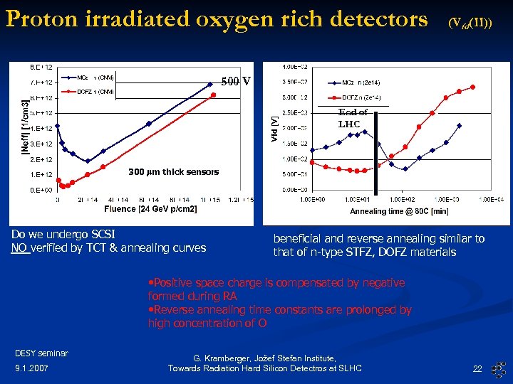 Proton irradiated oxygen rich detectors (Vfd (II)) 500 V End of LHC 300 mm thick sensors Do we undergo SCSI NO verified by TCT & annealing curves beneficial and reverse annealing similar to that of n-type STFZ, DOFZ materials • Positive space charge is compensated by negative formed during RA • Reverse annealing time constants are prolonged by high concentration of O DESY seminar 9. 1. 2007 G. Kramberger, Jožef Stefan Institute, Towards Radiation Hard Silicon Detectros at SLHC 22
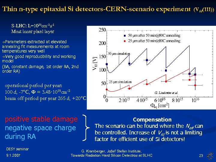 Thin n-type epitaxial Si detectors-CERN-scenario experiment (Vfd (III)) S-LHC: L=1035 cm-2 s-1 Most inner pixel layer àParameters extracted at elevated annealing fit measurements at room temperatures very well àVery good reproducibility and working model (BA, constant damage, 1 st order RA, 2 nd order RA) operational period per year: 100 d, -7°C, Φ = 3. 48· 1015 cm-2 beam off period per year 265 d, +20°C positive stable damage negative space charge during RA DESY seminar 9. 1. 2007 G. Lindström et al. Compensation The scenario can be found where the Neff can be controlled. Increase of Vfd is not a limiting factor for efficient use of Si detectors! G. Kramberger, Jožef Stefan Institute, Towards Radiation Hard Silicon Detectros at SLHC 23
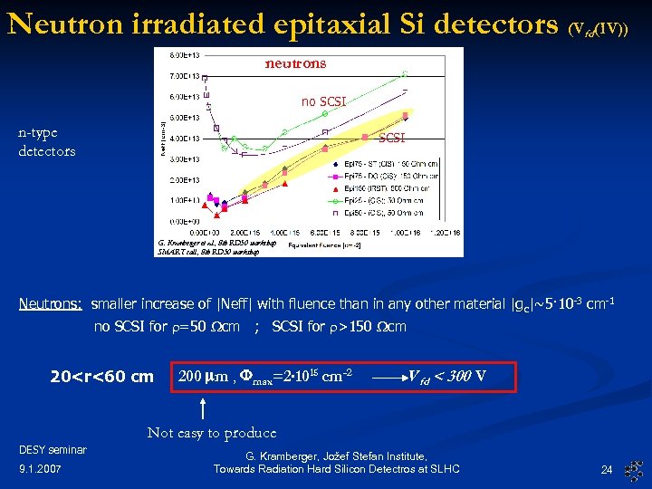 Neutron irradiated epitaxial Si detectors (V fd (IV)) neutrons no SCSI n-type detectors SCSI G. Kramberger et al. , 8 th RD 50 workshop SMART coll. , 8 th RD 50 workshop Neutrons: smaller increase of |Neff| with fluence than in any other material |g c|~5· 10 -3 cm-1 no SCSI for r=50 Wcm ; SCSI for r>150 Wcm 20
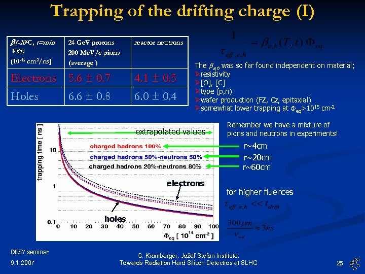 Trapping of the drifting charge (I) b(-10 o. C, t=min Vfd) [10 -16 cm 2/ns] 24 Ge. V protons 200 Me. V/c pions (average ) Electrons 5. 6 ± 0. 7 Holes 6. 6 ± 0. 8 reactor neutrons 4. 1 ± 0. 5 6. 0 ± 0. 4 The be, h was so far found independent on material; Øresistivity Ø[O], [C] Øtype (p, n) Øwafer production (FZ, Cz, epitaxial) Øsomewhat lower trapping at Feq>1015 cm-2 extrapolated values Remember we have a mixture of pions and neutrons in experiments! r~4 cm r~20 cm r~60 cm electrons for higher fluences holes DESY seminar 9. 1. 2007 G. Kramberger, Jožef Stefan Institute, Towards Radiation Hard Silicon Detectros at SLHC 25
![Trapping of the drifting charge (II) tan @60 o. C Neutron irr. Eta[e. V] Trapping of the drifting charge (II) tan @60 o. C Neutron irr. Eta[e. V]](https://present5.com/presentation/c315e0527fb70dbc477771d317466c9d/image-26.jpg) Trapping of the drifting charge (II) tan @60 o. C Neutron irr. Eta[e. V] Electrons 0. 3± 0. 15 ~650 min 1. 06± 0. 1 Holes -0. 4± 0. 2 ~550 min 0. 98± 0. 1 Confirmed also by ATLAS pixel test beam! T. Lari, Nucl. Inst. Meth. A 518 (2004) 349. Trapping probability decreases with temperature, but mobility also! Operation at lower T doesn’t improve CCE ! DESY seminar 9. 1. 2007 G. Kramberger, Jožef Stefan Institute, Towards Radiation Hard Silicon Detectros at SLHC 26
Trapping of the drifting charge (II) tan @60 o. C Neutron irr. Eta[e. V] Electrons 0. 3± 0. 15 ~650 min 1. 06± 0. 1 Holes -0. 4± 0. 2 ~550 min 0. 98± 0. 1 Confirmed also by ATLAS pixel test beam! T. Lari, Nucl. Inst. Meth. A 518 (2004) 349. Trapping probability decreases with temperature, but mobility also! Operation at lower T doesn’t improve CCE ! DESY seminar 9. 1. 2007 G. Kramberger, Jožef Stefan Institute, Towards Radiation Hard Silicon Detectros at SLHC 26
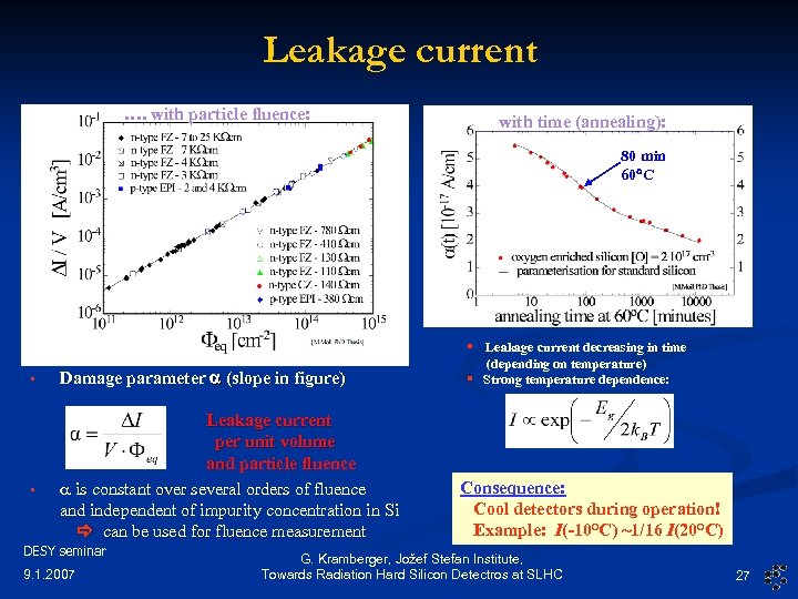 Leakage current …. with particle fluence: with time (annealing): 80 min 60 C § Leakage current decreasing in time § § Damage parameter (slope in figure) Leakage current per unit volume and particle fluence is constant over several orders of fluence and independent of impurity concentration in Si can be used for fluence measurement DESY seminar 9. 1. 2007 (depending on temperature) § Strong temperature dependence: Consequence: Cool detectors during operation! Example: I(-10°C) ~1/16 I(20°C) G. Kramberger, Jožef Stefan Institute, Towards Radiation Hard Silicon Detectros at SLHC 27
 Device engineering DESY seminar 9. 1. 2007 G. Kramberger, Jožef Stefan Institute, Towards Radiation Hard Silicon Detectros at SLHC 28
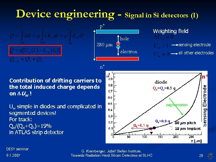 Device engineering - Signal in Si detectors (I) p+ 280 mm Weighting field hole sensing electrode electron all other electrodes n+ Contribution of drifting carriers to the total induced charge depends on DUw ! Uw simple in diodes and complicated in segmented devices! For track: Qe/(Qe+Qh)=19% in ATLAS strip detector DESY seminar 9. 1. 2007 G. Kramberger, Jožef Stefan Institute, Towards Radiation Hard Silicon Detectros at SLHC n+ diode Qh=Qe=0. 5 q segmentation 80 mm pitch 18 mm implant 29
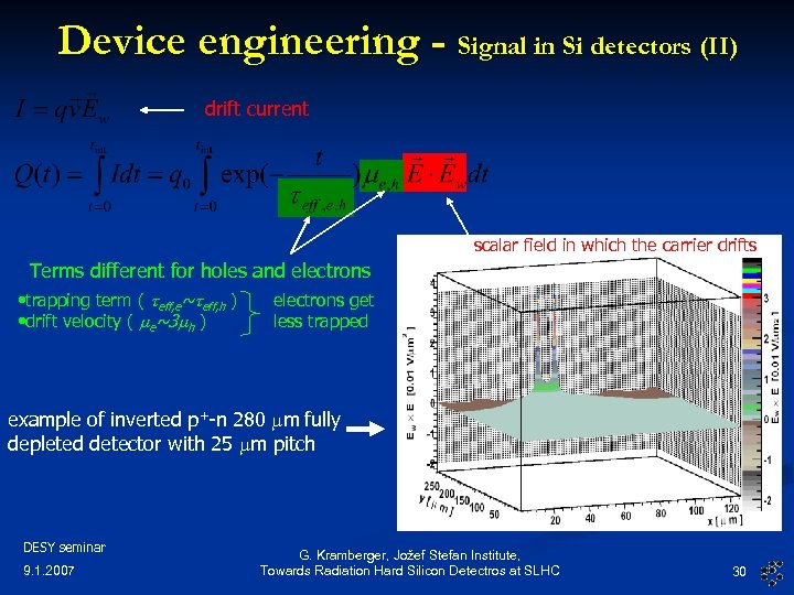 Device engineering - Signal in Si detectors (II) drift current scalar field in which the carrier drifts Terms different for holes and electrons • trapping term ( teff, e~teff, h ) • drift velocity ( me~3 mh ) electrons get less trapped example of inverted p+-n 280 mm fully depleted detector with 25 mm pitch DESY seminar 9. 1. 2007 G. Kramberger, Jožef Stefan Institute, Towards Radiation Hard Silicon Detectros at SLHC 30
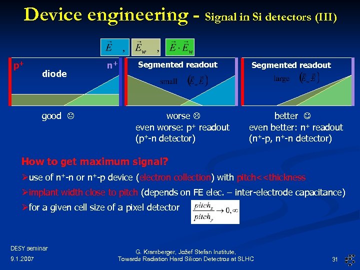 Device engineering - Signal in Si detectors (III) p+ diode good n+ Segmented readout worse even worse: p+ readout (p+-n detector) Segmented readout better even better: n+ readout (n+-p, n+-n detector) How to get maximum signal? Øuse of n+-n or n+-p device (electron collection) with pitch<
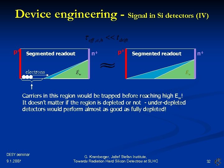 Device engineering - Signal in Si detectors (IV) p+ Segmented readout n+ electrons Carriers in this region would be trapped before reaching high E w! It doesn’t matter if the region is depleted or not - under-depleted detectors would perform almost as good as fully depleted! DESY seminar 9. 1. 2007 G. Kramberger, Jožef Stefan Institute, Towards Radiation Hard Silicon Detectros at SLHC 32
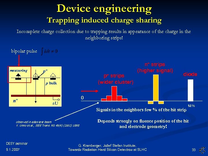 Device engineering Trapping induced charge sharing Incomplete charge collection due to trapping results in appearance of the charge in the neighboring strips! bipolar pulse measuring p+ p+ strips (wider cluster) p bulk n+ n+ strips (higher signal) diode 0 ±U Signals in the neighbors few % of the hit strip observed in atlas test beam Y. Unno et al. , IEEE Trans. NS 49(4) (2002) 1868 DESY seminar 9. 1. 2007 81% Depends strongly on fluence position of the hit and electrode geometry! G. Kramberger, Jožef Stefan Institute, Towards Radiation Hard Silicon Detectros at SLHC 33
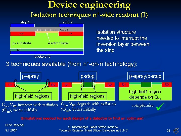 Device engineering Isolation techniques n+-side readout (I) strip 1 n+ strip 2 ++++ p- substrate oxide n+ isolation structure needed to interrupt the inversion layer between the strip electron layer p+ backplane 3 techniques available (from n+-on-n technology): p-stop p-spray S 1 S 2 high-field regions S 1 p-spray/p-stop S 2 S 1 high-field regions Cint, VBR improve with radiation Cint, VBR degrade with radiation (Oox), better initially (Oox), worse initially S 2 high-field region depends on Qox compromise Simulations needed for each design of a detector to find an optimum! DESY seminar 9. 1. 2007 G. Kramberger, Jožef Stefan Institute, Towards Radiation Hard Silicon Detectros at SLHC 34
 Silicon detectors for SLHC DESY seminar 9. 1. 2007 G. Kramberger, Jožef Stefan Institute, Towards Radiation Hard Silicon Detectros at SLHC 35
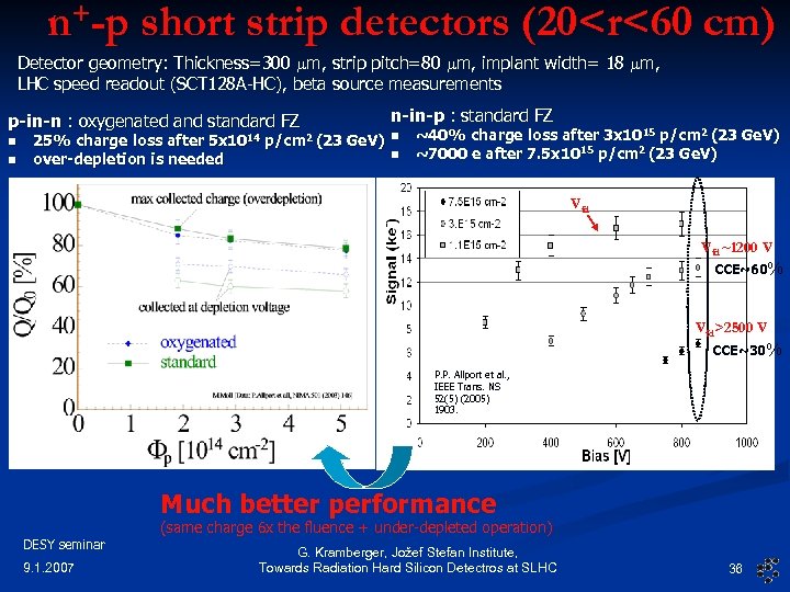 n+-p short strip detectors (20
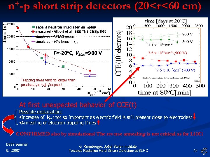 n+-p short strip detectors (20
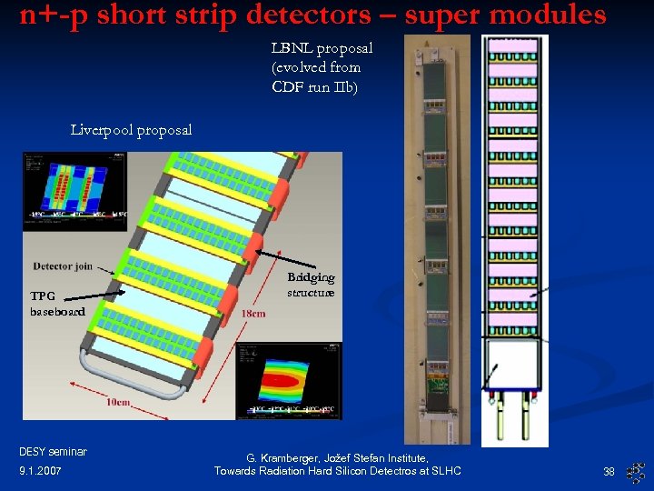 n+-p short strip detectors – super modules LBNL proposal (evolved from CDF run IIb) Liverpool proposal TPG baseboard DESY seminar 9. 1. 2007 Bridging structure G. Kramberger, Jožef Stefan Institute, Towards Radiation Hard Silicon Detectros at SLHC 38
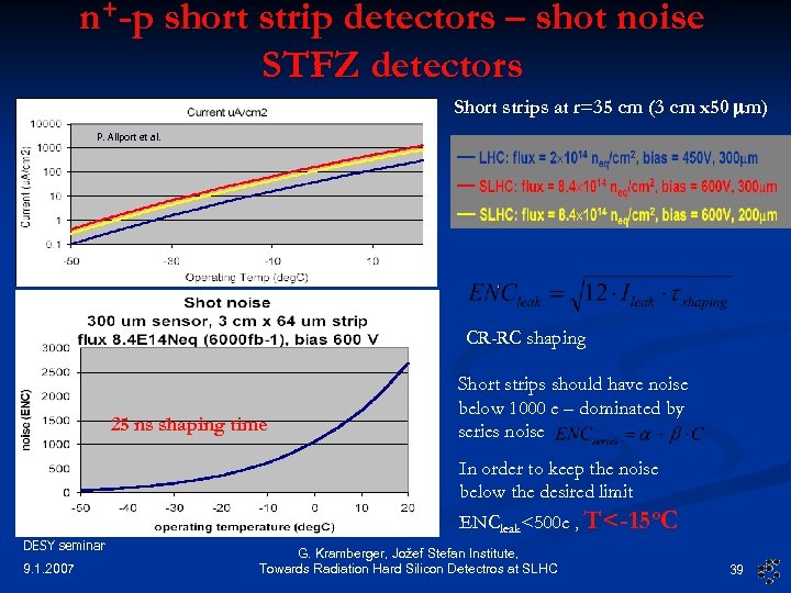 n+-p short strip detectors – shot noise STFZ detectors Short strips at r=35 cm (3 cm x 50 mm) P. Allport et al. CR-RC shaping 25 ns shaping time Short strips should have noise below 1000 e – dominated by series noise In order to keep the noise below the desired limit ENCleak<500 e , T<-15 o. C DESY seminar 9. 1. 2007 G. Kramberger, Jožef Stefan Institute, Towards Radiation Hard Silicon Detectros at SLHC 39
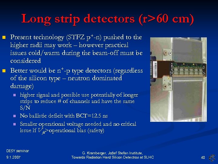 Long strip detectors (r>60 cm) n n Present technology (STFZ p+-n) pushed to the higher radii may work – however practical issues cold/warm during the beam-off must be considered Better would be n+-p type detectors (regardless of the silicon type – neutron dominated damage) n n n higher signal and possible use potentially of longer strips to reduce # of channels and have the same S/N No ballistic deficit with BCT=12. 5 ns Smaller operational voltage needed and no critical issue if Vfd>operational bias (safety) DESY seminar 9. 1. 2007 G. Kramberger, Jožef Stefan Institute, Towards Radiation Hard Silicon Detectros at SLHC 40
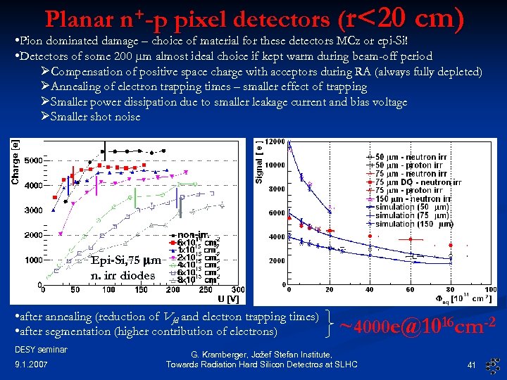 Planar n+-p pixel detectors (r<20 cm) • Pion dominated damage – choice of material for these detectors MCz or epi-Si! • Detectors of some 200 mm almost ideal choice if kept warm during beam-off period ØCompensation of positive space charge with acceptors during RA (always fully depleted) ØAnnealing of electron trapping times – smaller effect of trapping ØSmaller power dissipation due to smaller leakage current and bias voltage ØSmaller shot noise Epi-Si, 75 mm n. irr diodes • after annealing (reduction of Vfd and electron trapping times) • after segmentation (higher contribution of electrons) DESY seminar 9. 1. 2007 ~4000 e@1016 cm-2 G. Kramberger, Jožef Stefan Institute, Towards Radiation Hard Silicon Detectros at SLHC 41
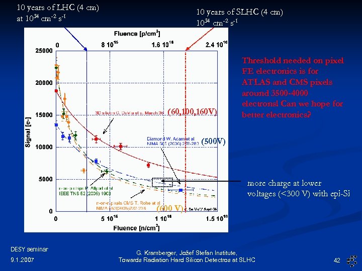 10 years of LHC (4 cm) at 1034 cm-2 s-1 10 years of SLHC (4 cm) 1034 cm-2 s-1 (60, 100, 160 V) Threshold needed on pixel FE electronics is for ATLAS and CMS pixels around 3500 -4000 electrons! Can we hope for better electronics? (500 V) more charge at lower voltages (<300 V) with epi-Si (600 V) DESY seminar 9. 1. 2007 G. Kramberger, Jožef Stefan Institute, Towards Radiation Hard Silicon Detectros at SLHC 42
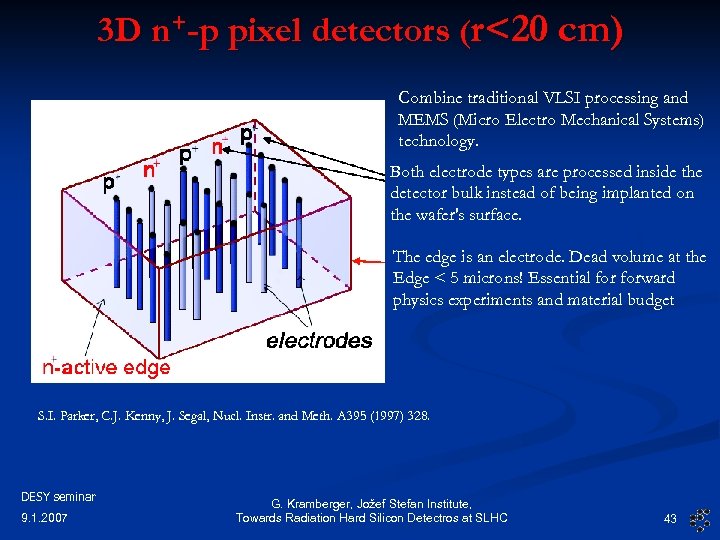 3 D n+-p pixel detectors (r<20 cm) Combine traditional VLSI processing and MEMS (Micro Electro Mechanical Systems) technology. Both electrode types are processed inside the detector bulk instead of being implanted on the wafer's surface. The edge is an electrode. Dead volume at the Edge < 5 microns! Essential forward physics experiments and material budget S. I. Parker, C. J. Kenny, J. Segal, Nucl. Instr. and Meth. A 395 (1997) 328. DESY seminar 9. 1. 2007 G. Kramberger, Jožef Stefan Institute, Towards Radiation Hard Silicon Detectros at SLHC 43
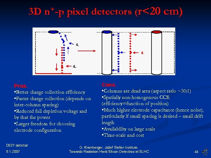 3 D n+-p pixel detectors (r<20 cm) Pros. • Better charge collection efficiency • Faster charge collection (depends on inter-column spacing) • Reduced full depletion voltage and by that the power • Larger freedom for choosing electrode configuration DESY seminar 9. 1. 2007 Cons. • Columns are dead area (aspect ratio ~30: 1) • Spatially non-homogenous CCE (efficiency=function of position) • Much higher electrode capacitance (hence noise), particularly if small spacing is desired – small drift length • Availability on large scale • Time-scale and cost G. Kramberger, Jožef Stefan Institute, Towards Radiation Hard Silicon Detectros at SLHC 44
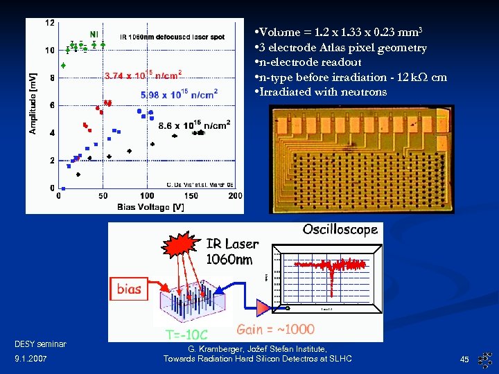 • Volume = 1. 2 x 1. 33 x 0. 23 mm 3 • 3 electrode Atlas pixel geometry • n-electrode readout • n-type before irradiation - 12 k. W cm • Irradiated with neutrons DESY seminar 9. 1. 2007 G. Kramberger, Jožef Stefan Institute, Towards Radiation Hard Silicon Detectros at SLHC 45
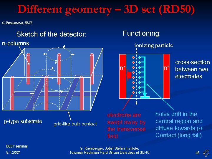 Different geometry – 3 D sct (RD 50) C. Piemonte et al. , IRST Sketch of the detector: Functioning: n-columns ionizing particle n+ p-type substrate DESY seminar 9. 1. 2007 grid-like bulk contact electrons are swept away by the transversal field G. Kramberger, Jožef Stefan Institute, Towards Radiation Hard Silicon Detectros at SLHC n+ cross-section between two electrodes holes drift in the central region and diffuse towards p+ Contact (long tail) 46
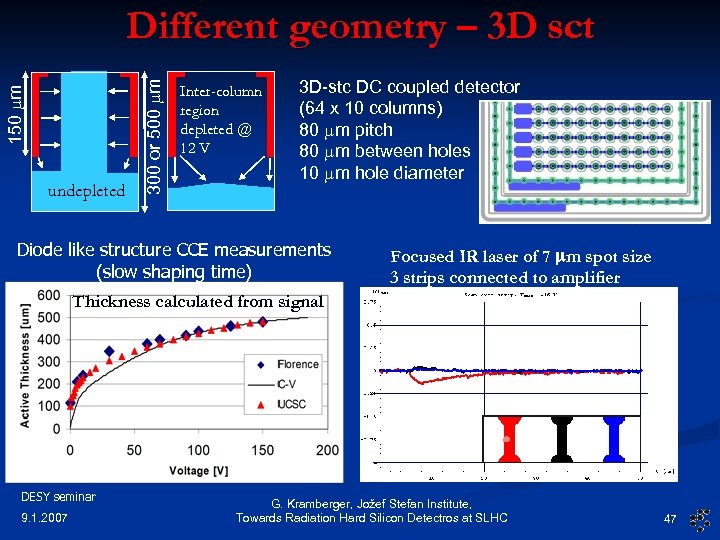 undepleted 300 or 500 mm 150 mm Different geometry – 3 D sct Inter-column region depleted @ 12 V 3 D-stc DC coupled detector (64 x 10 columns) 80 mm pitch 80 mm between holes 10 mm hole diameter Diode like structure CCE measurements (slow shaping time) Focused IR laser of 7 mm spot size 3 strips connected to amplifier Thickness calculated from signal DESY seminar 9. 1. 2007 G. Kramberger, Jožef Stefan Institute, Towards Radiation Hard Silicon Detectros at SLHC 47
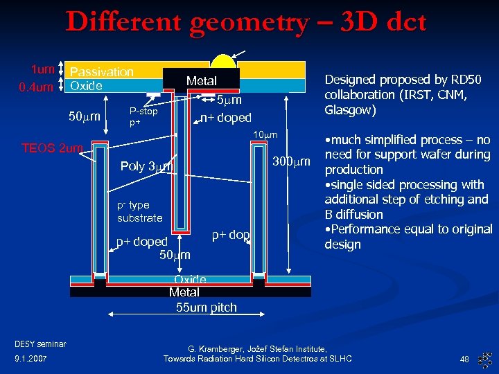 Different geometry – 3 D dct 1 um 0. 4 um Passivation Oxide 50 mm Designed proposed by RD 50 collaboration (IRST, CNM, Glasgow) Metal 5 mm n+ doped P-stop p+ 10 mm TEOS 2 um 300 mm Poly 3 mm p- type substrate p+ doped 50 mm p+ doped • much simplified process – no need for support wafer during production • single sided processing with additional step of etching and B diffusion • Performance equal to original design Oxide Metal 55 um pitch DESY seminar 9. 1. 2007 G. Kramberger, Jožef Stefan Institute, Towards Radiation Hard Silicon Detectros at SLHC 48
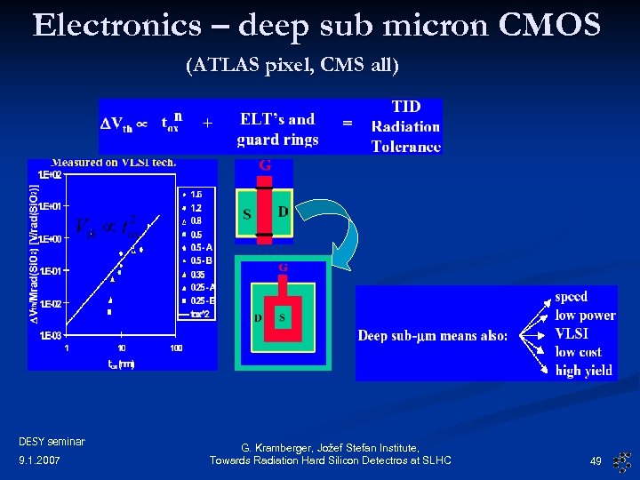 Electronics – deep sub micron CMOS (ATLAS pixel, CMS all) DESY seminar 9. 1. 2007 G. Kramberger, Jožef Stefan Institute, Towards Radiation Hard Silicon Detectros at SLHC 49
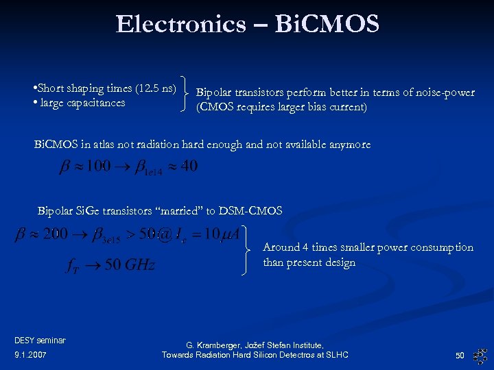 Electronics – Bi. CMOS • Short shaping times (12. 5 ns) • large capacitances Bipolar transistors perform better in terms of noise-power (CMOS requires larger bias current) Bi. CMOS in atlas not radiation hard enough and not available anymore Bipolar Si. Ge transistors “married” to DSM-CMOS Around 4 times smaller power consumption than present design DESY seminar 9. 1. 2007 G. Kramberger, Jožef Stefan Institute, Towards Radiation Hard Silicon Detectros at SLHC 50
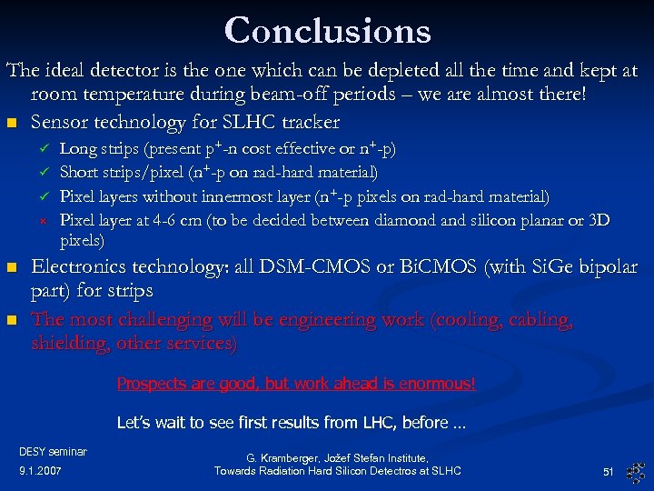 Conclusions The ideal detector is the one which can be depleted all the time and kept at room temperature during beam-off periods – we are almost there! n Sensor technology for SLHC tracker û n n Long strips (present p+-n cost effective or n+-p) Short strips/pixel (n+-p on rad-hard material) Pixel layers without innermost layer (n+-p pixels on rad-hard material) Pixel layer at 4 -6 cm (to be decided between diamond and silicon planar or 3 D pixels) Electronics technology: all DSM-CMOS or Bi. CMOS (with Si. Ge bipolar part) for strips The most challenging will be engineering work (cooling, cabling, shielding, other services) Prospects are good, but work ahead is enormous! Let’s wait to see first results from LHC, before … DESY seminar 9. 1. 2007 G. Kramberger, Jožef Stefan Institute, Towards Radiation Hard Silicon Detectros at SLHC 51


