faa1576b3b912fb1326f770114122452.ppt
- Количество слайдов: 58
 OPTIMAL ELECTRONIC CIRCUITS and MICROSYSTEMS NETWORKED DESIGNER Prof. ANATOLY PETRENKO National Technical University of Ukraine “Kiev Polytechnic Institute”, Tel. /FAX +380 44 280 90 46, e-mail: petrenko@cad. kiev. ua SW, EB, Grid
 Outline • Networked CAD tools • International co-operation Experience • ALLTED – All Technology Designer • Novel numerical methods • Results of solving the benchmark circuits • Optimization example • AND Logical Circuit on OET • Possible co-operation SW, EB, Grid 2
 Networked CAD tools Remote access to CAD tools and collectively execution the joint Projects ; • Meeting different requirements to hardware of a server and a client ; • New level of functional cooperation via GRID infrastructure; • Possibilities for Small and Middle enterprises to take a part in international work force distribution developing competitive products. • SW, EB, Grid 3
 ALLTED – All Technology Designer Previous versions of this system (named SPARS, PRAM-01, PRAM-PK, PRANS for EC and SM computers) were used in the former Soviet Union as the branch Ministry of the Defense industry standard OST V 3 -4776 -80 for circuit design automation and similar standards for the Ministries of General and Average Machinobuilding and Radio industry. ALLTED is especially useful in the development of new products which combine various physical phenomena in one device SW, EB, Grid 4
 International co-operation Experience • Digital (Alpha Processor simulation) • Intel (Parallel computation, Formal verification, Layout extraction, VLSI Interconnects Model-Order Reduction , ALOE to Cadence / Cadence to ALOE converters ) • General Electric (MEMS Model design) • Motorola ( Signal Processors implementation) • Sun ( Layout verification) • Panasonic (Remote Access to Networked Appliances ) • • Melexes (VLSI design with 0. 25 u) HPC –Germany ( RF circuits design) EC Projects ( Tempus, Inco- Copernicus) STCU Projects ( Remote Simulation, MEMS Design) SW, EB, Grid 5
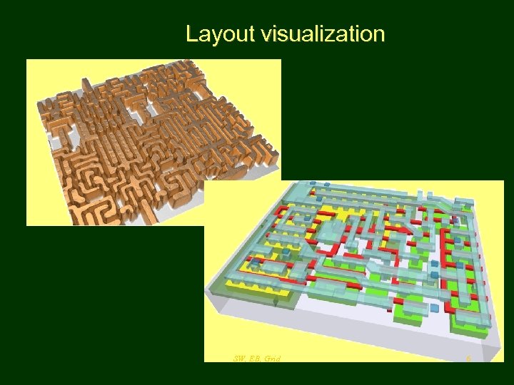 Layout visualization SW, EB, Grid 6
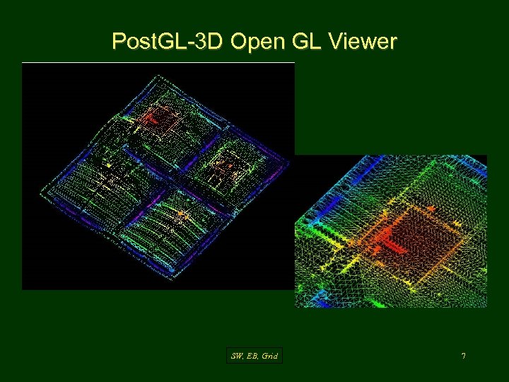 Post. GL-3 D Open GL Viewer SW, EB, Grid 7
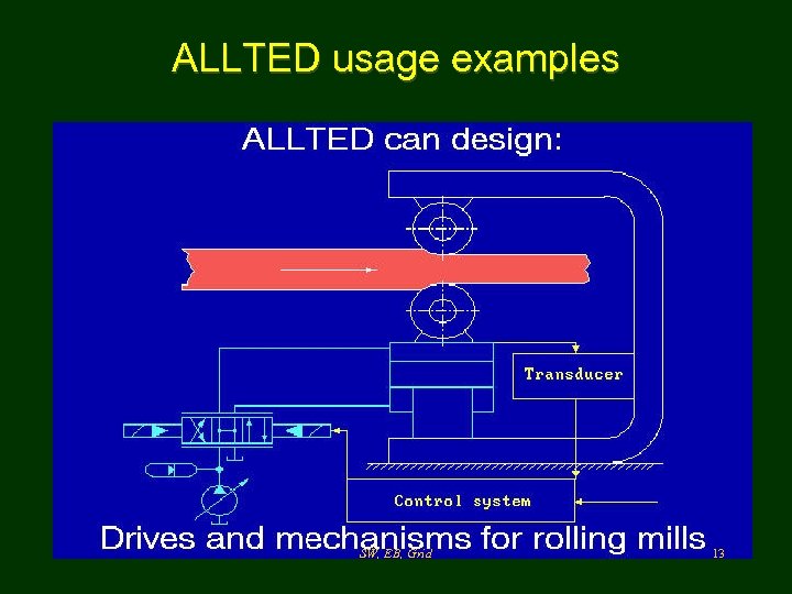
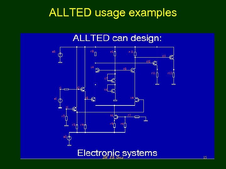
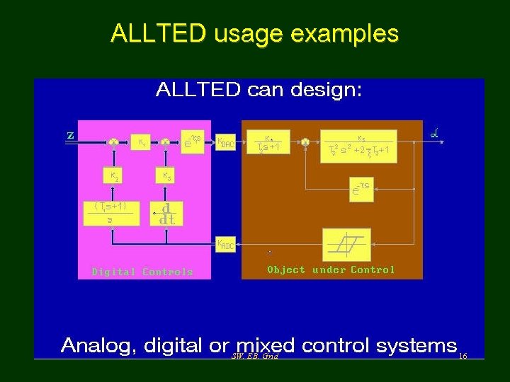
 ALLTED – All Technology Designer • ALLTED is an acronym for ALL TEchnology Designer. It was developed not only for simulation and analysis, but for processing project procedures such as: – parametric optimization tasks; – optimal tolerance assignments; – centering availability regions; – yield maximization; – design of Nonlinear Dynamic Systems composed of either/and electronic, hydraulic, pneumatic, mechanical, electromagnetic, and other elements. SW, EB, Grid 8
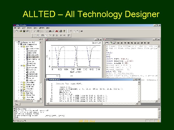 ALLTED – All Technology Designer SW, EB, Grid 9
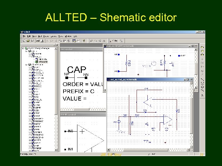 ALLTED – Shematic editor SW, EB, Grid 10
 ALLTED in distributed Web environment SW, EB, Grid 11
 ALLTED usage examples SW, EB, Grid 12
 ALLTED usage examples SW, EB, Grid 13
 ALLTED usage examples SW, EB, Grid 14
 ALLTED usage examples SW, EB, Grid 15
 ALLTED usage examples SW, EB, Grid 16
 ALLTED usage examples SW, EB, Grid 17
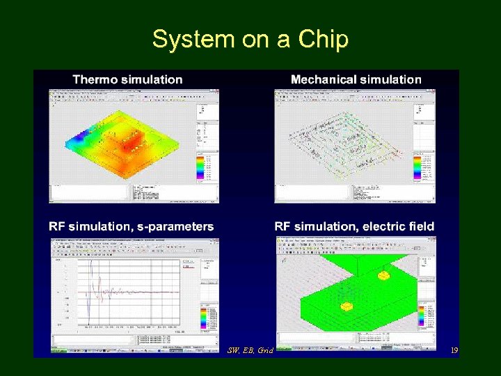
 System on a Chip SW, EB, Grid 18
 System on a Chip SW, EB, Grid 19
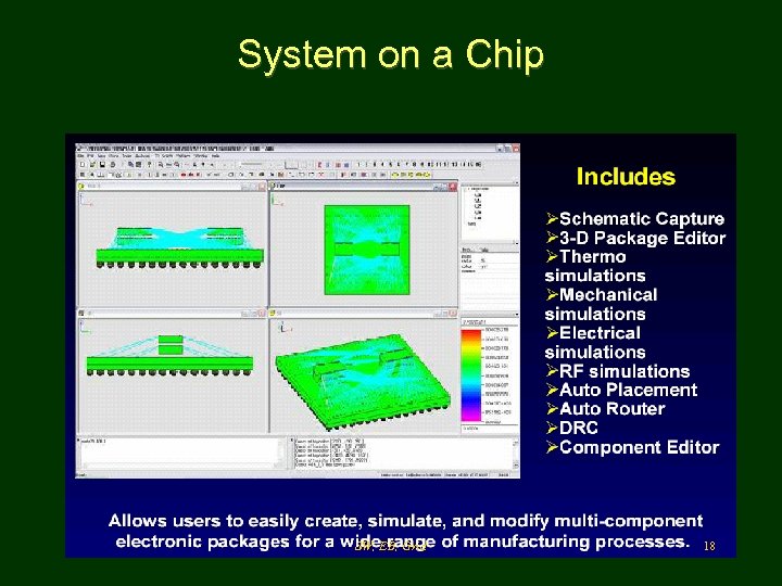
 ALLTED offers: • • • Faster simulation speed and improved numerical convergence; Sensitivity analysis for frequency and transient analyses; Comprehensive optimization procedure and optimal tolerances assignment ; Alternative approach to the secondary response parameters determination (delays, rise and fall times, etc. ); Powerful user-defined modeling capability. Original way of generating a system-level model of MEMS from FEM component equations. SW, EB, Grid 20
 Novel numerical methods • The new solution curve-search method for Steady State (DC) Analysis which provides the quick descent to the solution point region from any starting point • The Diagonal Modification Method which helps considerably preserve convergence of linearized equations solution without re-ordering when matrix element values change from one iteration to another iteration. • The Optimization Variable-order Methods which is equivalent to taking into consideration five terms of Tailor’s series for the Goal function which considerably improve determination of a direction to the optimal point SW, EB, Grid 21
 Novel numerical methods • The Implicit Linear Multi-step Variable-order Integration Method for Transient Analysis(TR) which uses high order back differences that allows to select the proper one resulting in minimization of solution time for prescribed accuracy. • The Optimal Tolerances Assignment Method which is based on applying Optimization procedures and takes into account the prescribed deviations of Controlled Output Parameters • Statistical Yield Maximization Method which provides “centering” the solution point in the region of acceptable solutions SW, EB, Grid 22
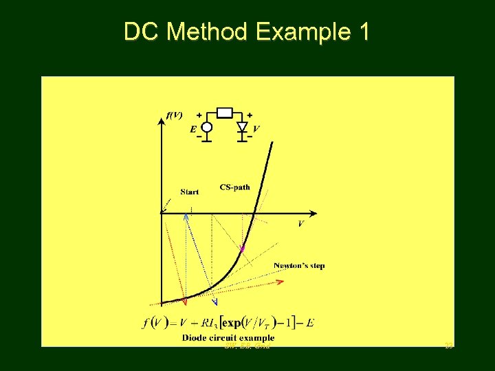 DC Method Example 1 SW, EB, Grid 23
 Diagonal modification method SW, EB, Grid 24
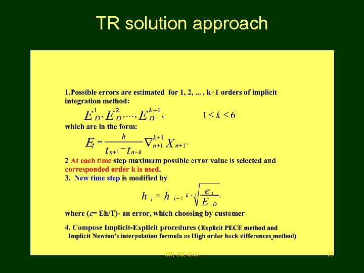 TR solution approach SW, EB, Grid 25
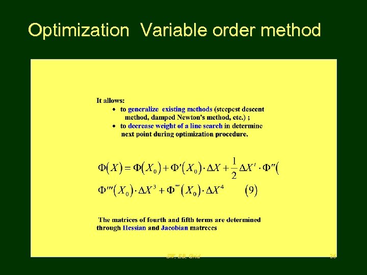 Optimization Variable order method SW, EB, Grid 26
 INTEL AWARD Конкурс исследовательских проектов области автоматизации Проектирования интегральных схем награждается ПЕТРЕНКО АНАТОЛИЙ ИВАНОВИЧ Национальный Технический Университет Украины «Киевский политехнический институт ПРОЕКТ Разработка эффективных численных методов моделирования и оптимизации схемотехнических решений для СБИС SW, EB, Grid 27
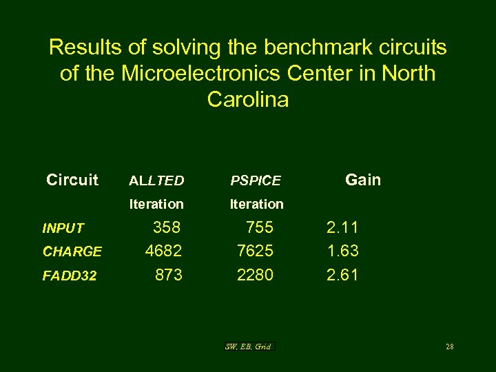 Results of solving the benchmark circuits of the Microelectronics Center in North Carolina Circuit CHARGE FADD 32 PSPICE Iteration INPUT ALLTED Gain Iteration 358 4682 873 755 7625 2280 SW, EB, Grid 2. 11 1. 63 2. 61 28
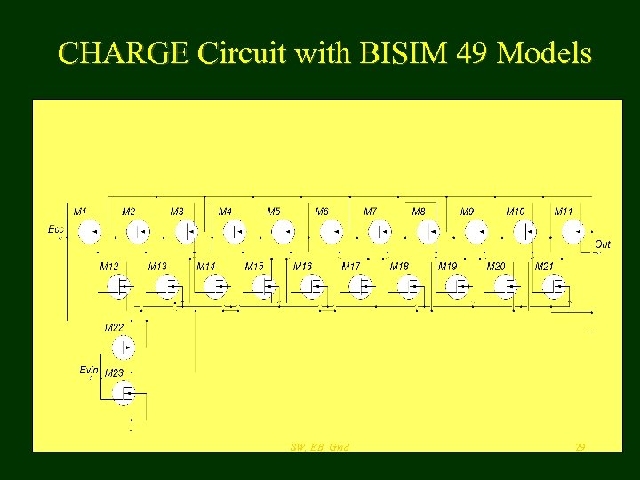 CHARGE Circuit with BISIM 49 Models SW, EB, Grid 29
 ALLTED and PSPICE v. 9. 2 outputs: SW, EB, Grid 30
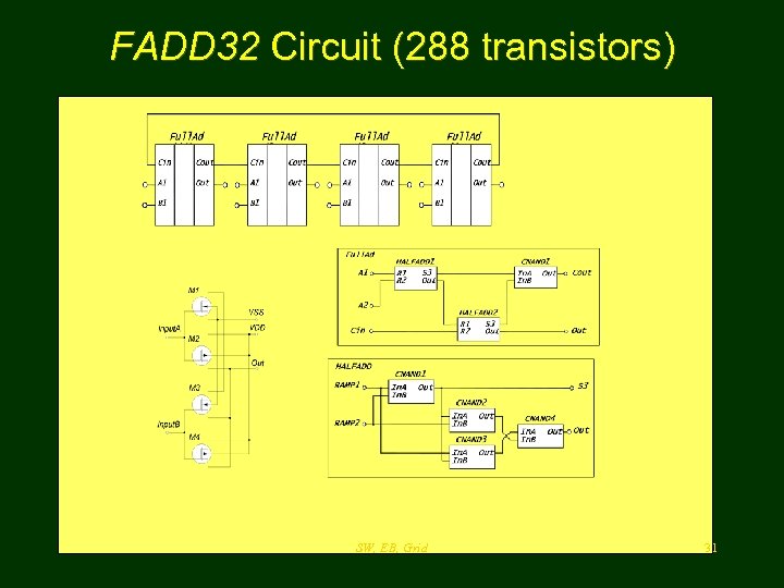 FADD 32 Circuit (288 transistors) SW, EB, Grid 31
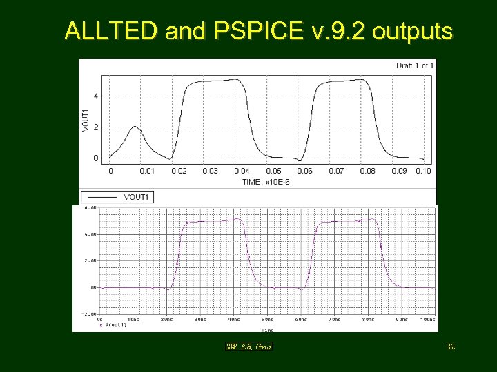 ALLTED and PSPICE v. 9. 2 outputs SW, EB, Grid 32
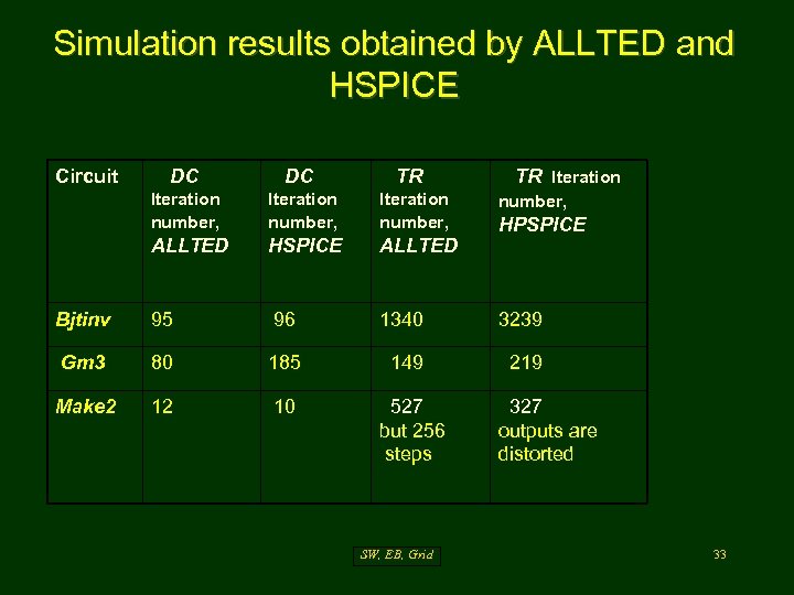 Simulation results obtained by ALLTED and HSPICE Circuit DC DC TR Iteration number, ALLTED HSPICE ALLTED Bjtinv 95 96 1340 3239 Gm 3 80 185 149 219 Make 2 12 10 527 but 256 steps SW, EB, Grid TR Iteration number, HPSPICE 327 outputs are distorted 33
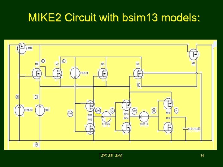 MIKE 2 Circuit with bsim 13 models: SW, EB, Grid 34
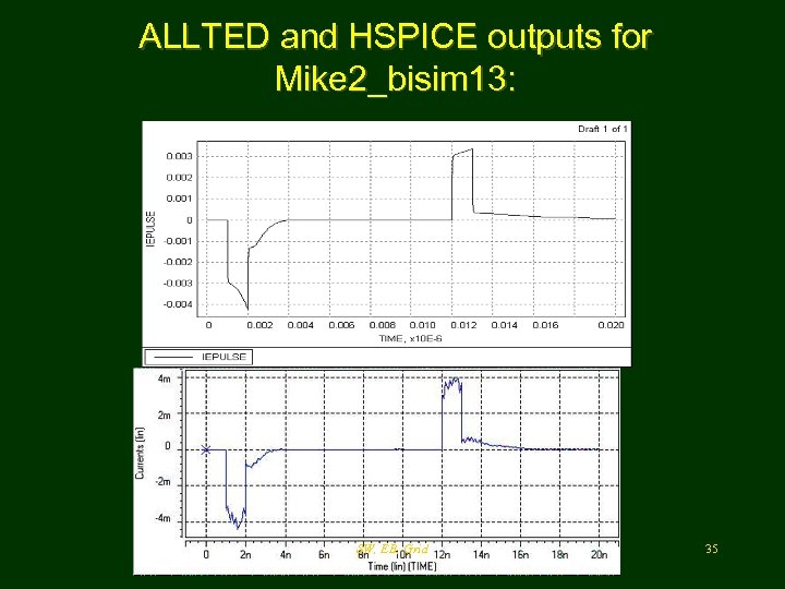 ALLTED and HSPICE outputs for Mike 2_bisim 13: SW, EB, Grid 35
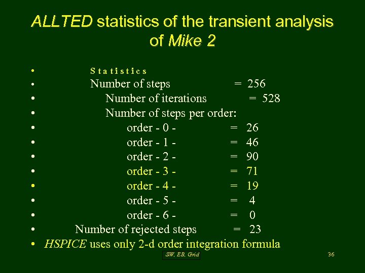 ALLTED statistics of the transient analysis of Mike 2 • • • • S t a t i s t i c s Number of steps = 256 Number of iterations = 528 Number of steps per order: order - 0 = 26 order - 1 = 46 order - 2 = 90 order - 3 = 71 order - 4 = 19 order - 5 = 4 order - 6 = 0 Number of rejected steps = 23 HSPICE uses only 2 -d order integration formula SW, EB, Grid 36
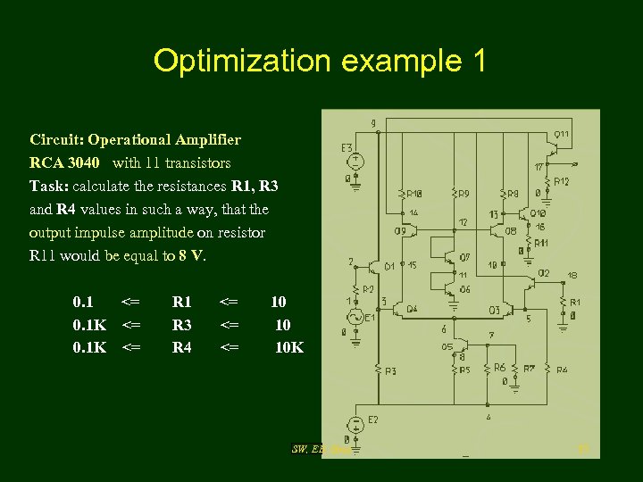 Optimization example 1 Circuit: Operational Amplifier RCA 3040 with 11 transistors Task: calculate the resistances R 1, R 3 and R 4 values in such a way, that the output impulse amplitude on resistor R 11 would be equal to 8 V. 0. 1 <= R 1 <= 10 0. 1 K <= R 3 <= 10 0. 1 K <= R 4 <= 10 K SW, EB, Grid 37
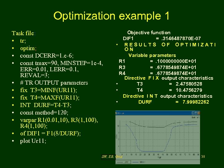 Optimization example 1 Task file: • tr; • optim; • const DCERR=1. e-6; • const tmax=90, MINSTEP=1 e-4, ERR=0. 01, LERR=0. 1, REVAL=3; • # TR OUTPUT parameters • fix T 3=MINF(UR 11); • fix T 4=MAXF(UR 11); • INT DURF=T 4 -T 3; • const method=120; • varpar R 1(0. 01, 10), R 3(1, 100), R 4(1, 100); • of DIF 1 = F 1(8/DURF); • plot Ur 11; Objective function DIF 1 =. 3146487870 E-07 • RESULTS OF OPTIMIZATI ON Variable parameters R 1 =. 100000 E+01 R 3 =. 6778549874 E+01 R 4 =. 6778549874 E+01 Directive F I X output characteristics • T 3 = 2. 47580528 • T 4 = 10. 4756279 Directive I N T output characteristics • DURF = 7. 99982262 SW, EB, Grid 38
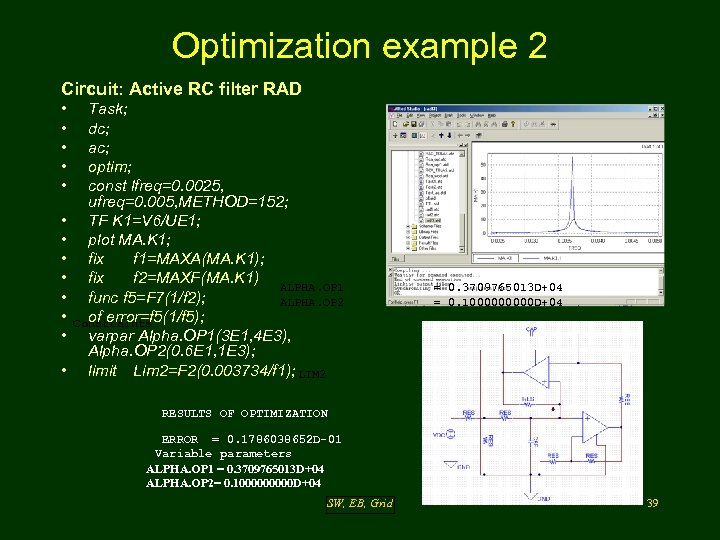 Optimization example 2 Circuit: Active RC filter RAD • • • • Task; dc; ac; optim; const lfreq=0. 0025, ufreq=0. 005, METHOD=152; TF K 1=V 6/UE 1; plot MA. K 1; fix f 1=MAXA(MA. K 1); fix f 2=MAXF(MA. K 1) ALPHA. OP 1 func f 5=F 7(1/f 2); ALPHA. OP 2 of error=f 5(1/f 5); Constraints varpar Alpha. OP 1(3 E 1, 4 E 3), Alpha. OP 2(0. 6 E 1, 1 E 3); limit Lim 2=F 2(0. 003734/f 1); LIM 2 = 0. 3709765013 D+04 = 0. 100000 D+04 RESULTS OF OPTIMIZATION ERROR = 0. 1786038652 D-01 Variable parameters ALPHA. OP 1 = 0. 3709765013 D+04 ALPHA. OP 2= 0. 100000 D+04 SW, EB, Grid 39
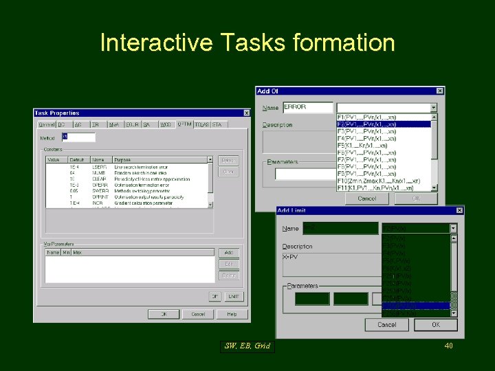 Interactive Tasks formation SW, EB, Grid 40
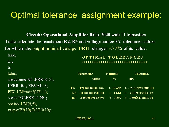 Optimal tolerance assignment example: Circuit: Operational Amplifier RCA 3040 with 11 transistors Task: calculate the resistances R 2, R 3 and voltage source E 2 tolerances values for which the output minimal voltage UR 11 changes +/- 5% of its value. task; dc; tr; tolas; const tmax=90 , ERR=0. 01, LERR=0. 1, REVAL=3; FIX UM=minf(UR 11); const TOLERR=0. 001; control UM(5, 5); varpar E 2(10), R 2, R 3(10); O P T I M A L T O L E R A N C E S ****************** Parameter Nominal Tolerance value % abs E 2 . 120000 E+02 +- 19. 682 +- -. 2361829758 E+01 R 2 . 1000000015 E+00 +- 4. 614 +- . 4613934550 E-02 R 3 . 100000 E+01 +- 3. 697 +- . 3696829081 E-01 SW, EB, Grid 41
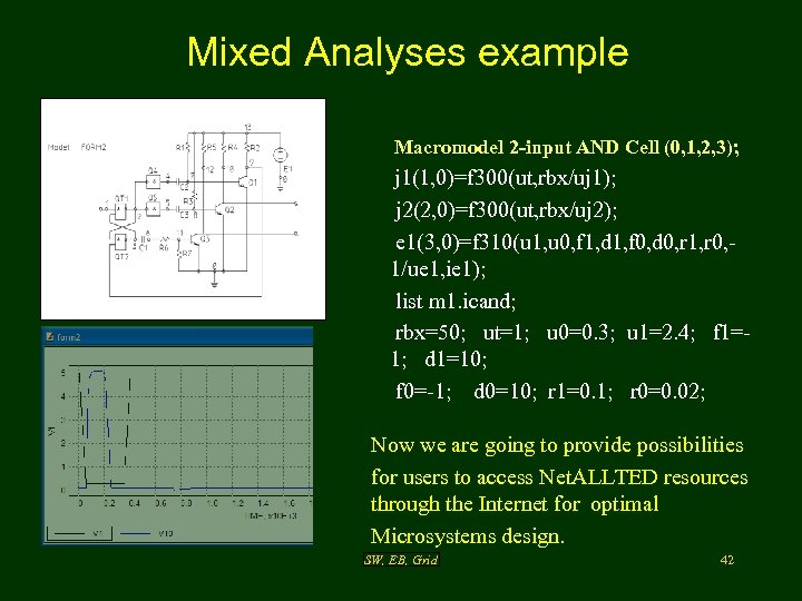 Mixed Analyses example Macromodel 2 -input AND Cell (0, 1, 2, 3); j 1(1, 0)=f 300(ut, rbx/uj 1); j 2(2, 0)=f 300(ut, rbx/uj 2); e 1(3, 0)=f 310(u 1, u 0, f 1, d 1, f 0, d 0, r 1, r 0, 1/ue 1, ie 1); list m 1. icand; rbx=50; ut=1; u 0=0. 3; u 1=2. 4; f 1=1; d 1=10; f 0=-1; d 0=10; r 1=0. 1; r 0=0. 02; Now we are going to provide possibilities for users to access Net. ALLTED resources through the Internet for optimal Microsystems design. SW, EB, Grid 42
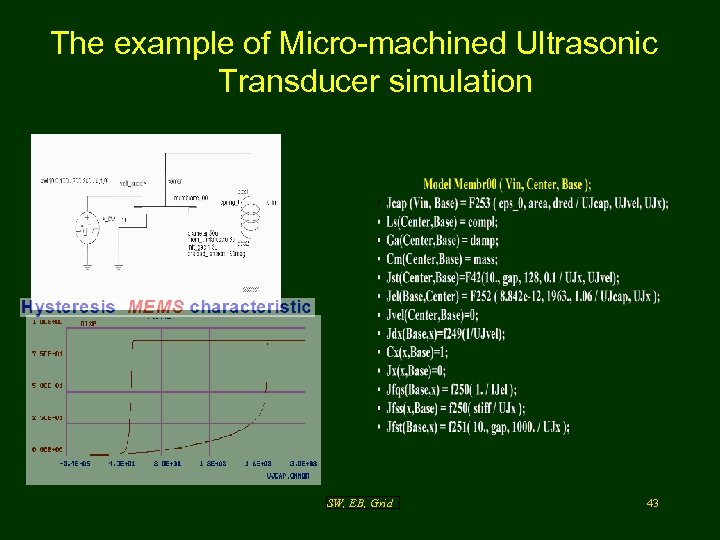 The example of Micro-machined Ultrasonic Transducer simulation SW, EB, Grid 43
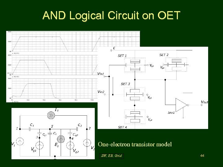 AND Logical Circuit on OET One-electron transistor model SW, EB, Grid 44
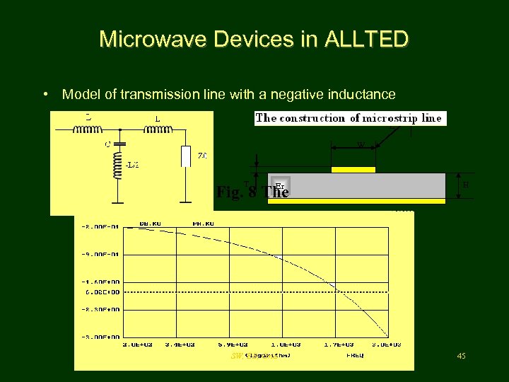 Microwave Devices in ALLTED • Model of transmission line with a negative inductance L W T Er Fig. 8 The SW, EB, Grid H 45
 ALLTED adaptation to a new application • New components mathematical models incorporating ( in equations form) • New graphical symbols for components, if any • New sections in library with components parameters • OF, LIMIT and FUNC libraries upgrading if any • Numerical procedures constants adjusting for new types of tasks SW, EB, Grid 46
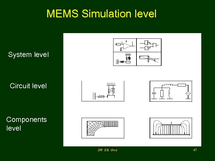 MEMS Simulation level System level Circuit level Components level SW, EB, Grid 47
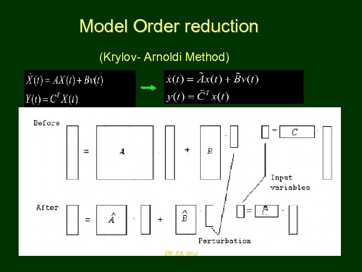 Model Order reduction (Krylov- Arnoldi Method) SW, EB, Grid
 Circuit model reduction method SW, EB, Grid 49
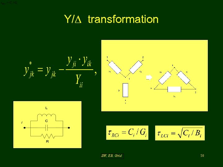 Y/∆ transformation SW, EB, Grid 50
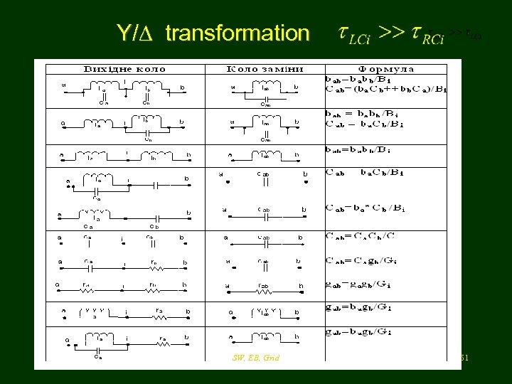 Y/∆ transformation Для складних 2 -х і 3 -х вимірних компонентів схемні моделі можуть мати дуже велику розмірність, ґтак що їхпорядок теж треба скорочувати SW, EB, Grid 51
 Y/∆ transformation Для складних 2 -х і 3 -х вимірних компонентів схемні моделі можуть мати дуже велику розмірність, ґтак що їхпорядок теж треба скорочувати SW, EB, Grid 52
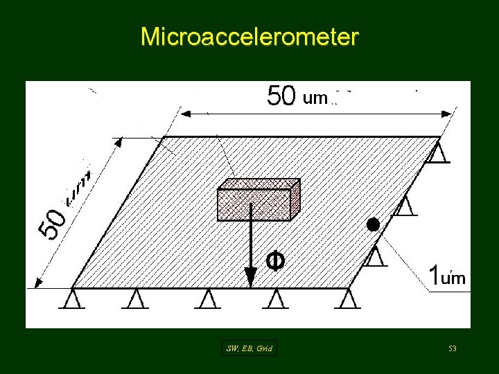 Microaccelerometer SW, EB, Grid 53
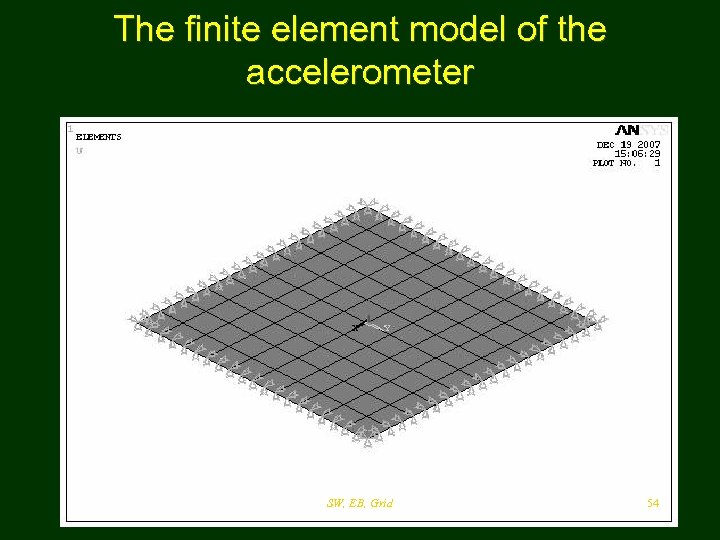 The finite element model of the accelerometer SW, EB, Grid 54
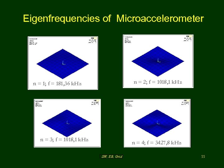 Eigenfrequencies of Microaccelerometer n = 2; f = 1018, 1 k. Hz n = 1; f = 181, 36 k. Hz n = 3; f = 1018, 1 k. Hz n = 4; f = 3427, 8 k. Hz SW, EB, Grid 55
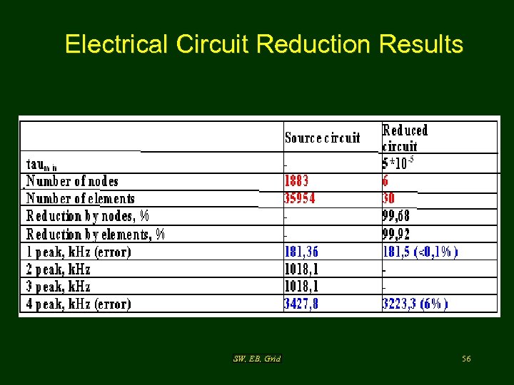 Electrical Circuit Reduction Results SW, EB, Grid 56
 Possible Project Tasks • ALLTED facilities Testing on Samsung Examples (optimization, tolerance assignment, yield maximization, DC conversion, RF design etc. ) • • Adaptation and enrichment of ALLTED component models Library (including new ones, say, for CCD , MEMS and IP Solutions), using semantic formats Developing parallel numerical simulation algorithms for a supercomputer Implementation of parallel ALLTED version in Grid environment and providing possibilities of remote its executing through Internet Development of the methodology of IC energy consumption minimization based on ALLTED optimization procedures (say, by varying W and L of transistors and keeping the given frequency value). SW, EB, Grid 57
 Thanks you very much ! SW, EB, Grid 58


