97331f64d00c28cdb4a14090365b086c.ppt
- Количество слайдов: 21
 Optical Patterned Defect Inspection to Extend Manufacturing Yield Rick Silver National Institute of Standards and Technology Surface and Microform Metrology Group B. Barnes Tool Design and Data Acquisition H. Zhou Simulation and Analysis Y. Sohn 193 nm Scatterfield Microscope R. Quintanilha 193 nm Tool Fabrication R. Attota Modeling and Analysis E. Marx Simulation Development Nanomanufacturing Metrology
 Outline • Defect inspection challenges • Scatterfield optical imaging fundamentals • Simulation techniques for intentional defect arrays • Polarization, scan axis, and wavelength sensitivity • Reduced dimensionality structures • Future directions Nanomanufacturing Metrology
 The Defect Inspection Challenge • Measuring sub-40 nm sized pattern defects throughout the entire chip. – 22 nm node has 11 nm defect requirements • Optical imaging methods used for full wafer defect inspection and SEM used for defect review. • There is a fundamental challenge in having nanometer scale resolution and wafer scale throughput. • The major semiconductor chip manufacturers have tagged this as a major obstacle to continued scaling and reducing cost per transistor. Nanomanufacturing Metrology
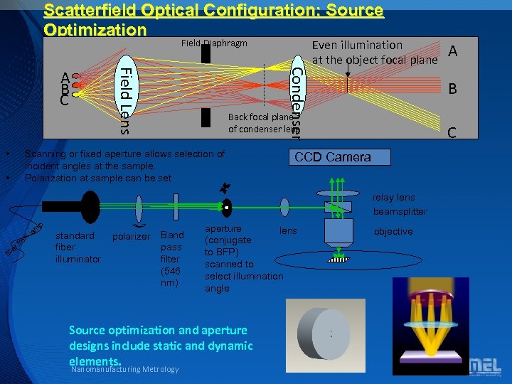 Scatterfield Optical Configuration: Source Optimization Field Diaphragm • Condenser Field Lens A B C C CCD Camera relay lens beamsplitter p om fr er fib m la standard fiber illuminator polarizer Band pass filter (546 nm) aperture lens (conjugate to BFP) scanned to select illumination angle Source optimization and aperture designs include static and dynamic elements. Nanomanufacturing Metrology A B Back focal plane of condenser lens Scanning or fixed aperture allows selection of incident angles at the sample. Polarization at sample can be set • Even illumination at the object focal plane objective
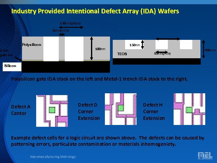 Industry Provided Intentional Defect Array (IDA) Wafers 130 nm(pitch) 35 nm(min) Polysilicon 2 nm gate ox 150 nm 100 nm TEOS 65 nm(min) Silicon Polysilicon gate IDA stack on the left and Metal-1 trench IDA stack to the right. Defect A Center Defect D Corner Extension Defect H Corner Extension Example defect cells for a logic circuit are shown above. The defects can be caused by patterning errors, particulate contamination or materials inhomogeniety. Nanomanufacturing Metrology 400 nm
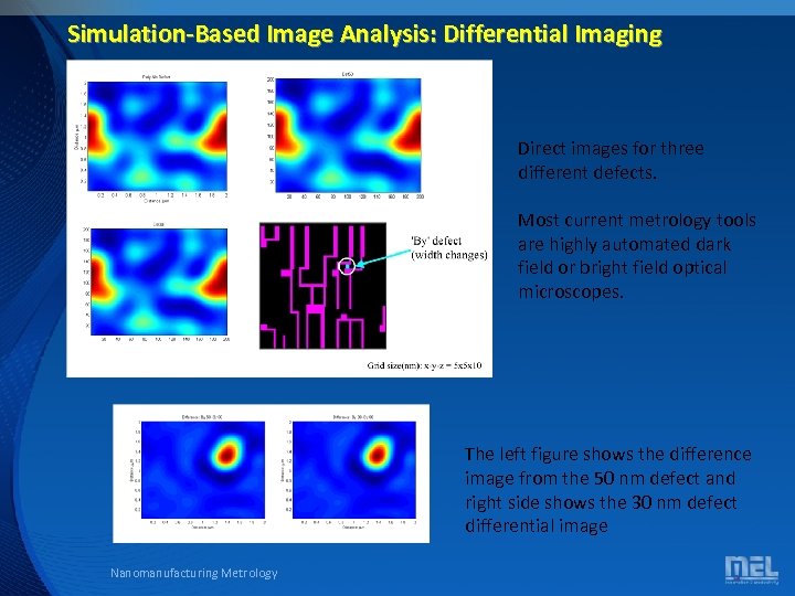 Simulation-Based Image Analysis: Differential Imaging Direct images for three different defects. Most current metrology tools are highly automated dark field or bright field optical microscopes. The left figure shows the difference image from the 50 nm defect and right side shows the 30 nm defect differential image Nanomanufacturing Metrology
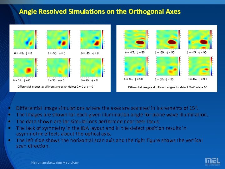 Angle Resolved Simulations on the Orthogonal Axes • • Differential image simulations where the axes are scanned in increments of 15 o. The images are shown for each given illumination angle for plane wave illumination. The data shown are for simulations performed near best focus. The lack of symmetry in the IDA layout and in the defect position results in asymmetric effects about the optical axis. • The left side shows the horizontal scan axis and the right figure shows the vertical scan direction. Nanomanufacturing Metrology
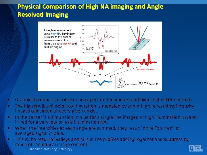 Physical Comparison of High NA imaging and Angle Resolved Imaging • Graphical comparison of scanning aperture techniques and fixed higher NA methods. • The high NA illumination configuration is modeled by summing the resulting intensity images calculated at every given angle. • In the center is a simulation in blue for a single line imaged at high illumination NA and in red for a very low on axis illumination NA. • When the intensities at each angle are summed, they result in the “blurred” or averaged signal in blue. • This is the result of valleys and hills in the profiles adding together and suppressing much of the optical image content. Nanomanufacturing Metrology
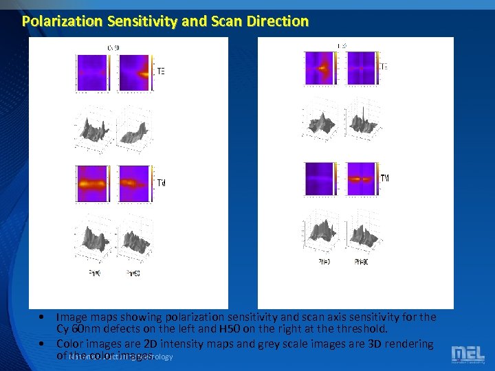 Polarization Sensitivity and Scan Direction • Image maps showing polarization sensitivity and scan axis sensitivity for the Cy 60 nm defects on the left and H 50 on the right at the threshold. • Color images are 2 D intensity maps and grey scale images are 3 D rendering of Nanomanufacturing Metrology the color images.
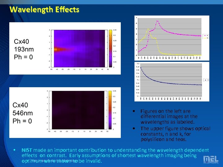 Wavelength Effects • Figures on the left are differential images at the wavelengths as labeled. • The upper figure shows optical constants, n and k, for polysilicon and teos. • NIST made an important contribution to understanding the wavelength dependent effects on contrast. Early assumptions of shortest wavelength imaging being Nanomanufacturing Metrology optimum were shown to be invalid.
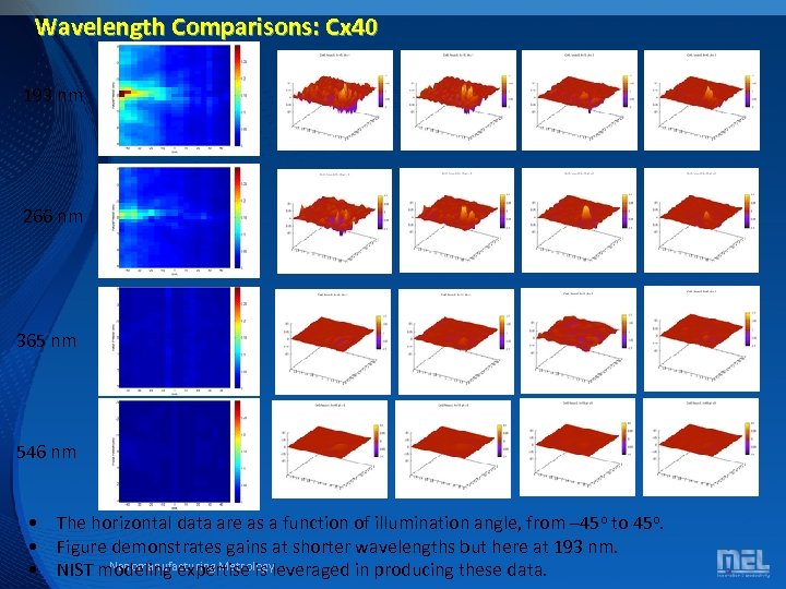 Wavelength Comparisons: Cx 40 193 nm 266 nm 365 nm 546 nm • The horizontal data are as a function of illumination angle, from – 45 o to 45 o. • Figure demonstrates gains at shorter wavelengths but here at 193 nm. Nanomanufacturing Metrology • NIST modeling expertise is leveraged in producing these data.
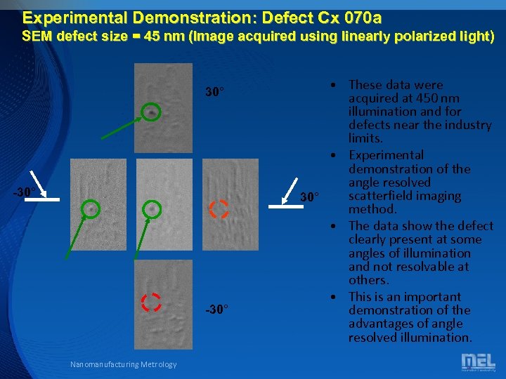 Experimental Demonstration: Defect Cx 070 a SEM defect size = 45 nm (Image acquired using linearly polarized light) 30° -30° Nanomanufacturing Metrology • These data were acquired at 450 nm illumination and for defects near the industry limits. • Experimental demonstration of the angle resolved scatterfield imaging 30° method. • The data show the defect clearly present at some angles of illumination and not resolvable at others. • This is an important demonstration of the advantages of angle resolved illumination.
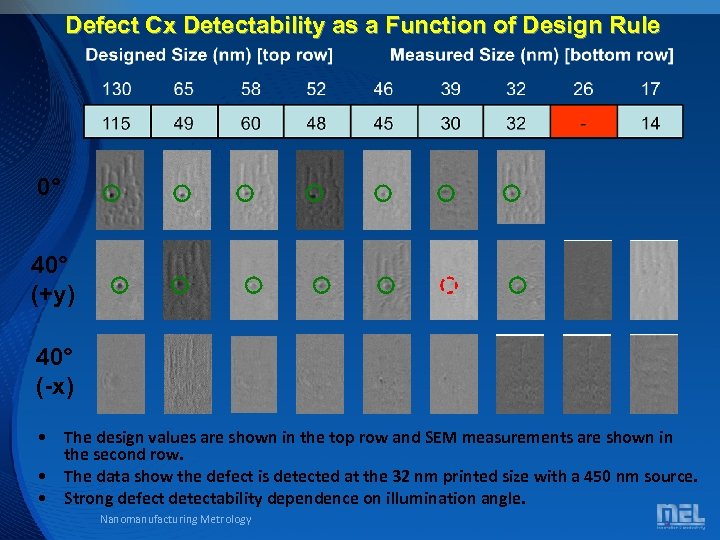 Defect Cx Detectability as a Function of Design Rule 0° 40° (+y) 40° (-x) • The design values are shown in the top row and SEM measurements are shown in the second row. • The data show the defect is detected at the 32 nm printed size with a 450 nm source. • Strong defect detectability dependence on illumination angle. Nanomanufacturing Metrology
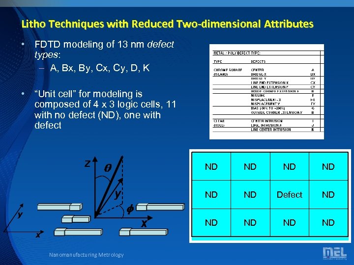 Litho Techniques with Reduced Two-dimensional Attributes • FDTD modeling of 13 nm defect types: – A, Bx, By, Cx, Cy, D, K • “Unit cell” for modeling is composed of 4 x 3 logic cells, 11 with no defect (ND), one with defect ND ND ND Defect ND ND Nanomanufacturing Metrology ND ND
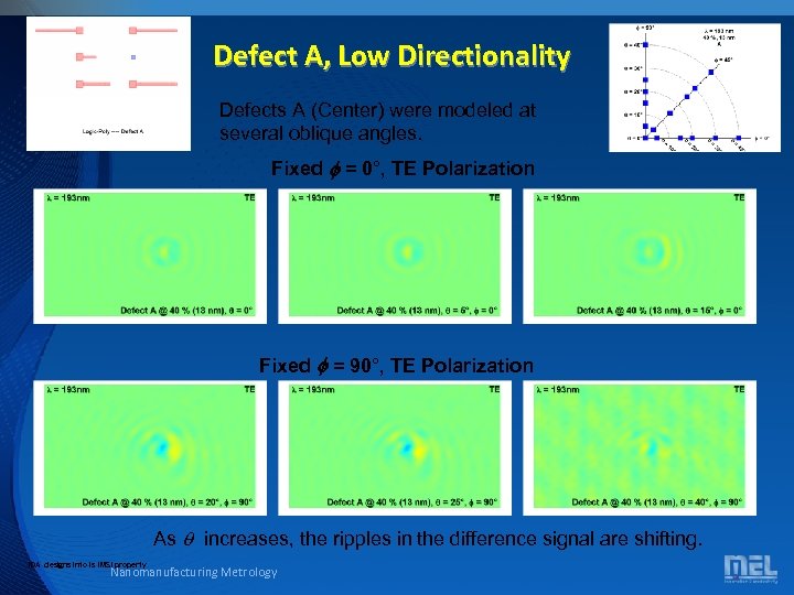 Defect A, Low Directionality Defects A (Center) were modeled at several oblique angles. Fixed f = 0°, TE Polarization Fixed f = 90°, TE Polarization As q increases, the ripples in the difference signal are shifting. IDA designs info is IMSI property Nanomanufacturing Metrology
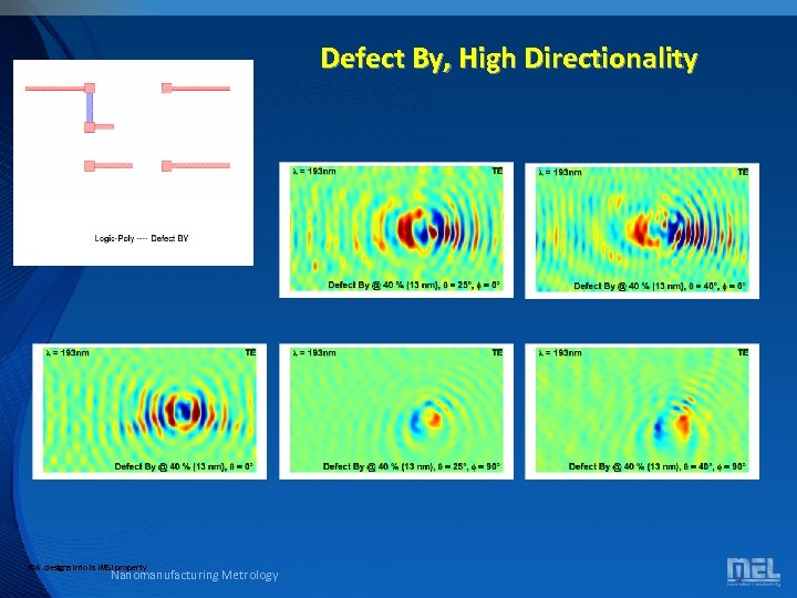 Defect By, High Directionality IDA designs info is IMSI property Nanomanufacturing Metrology
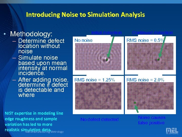 Introducing Noise to Simulation Analysis • Methodology: – Determine defect location without noise – Simulate noise based upon mean intensity at normal incidence. – After adding noise, determine if defect is detectable and where NIST expertise in modeling line edge roughness and sample variation has led to more realistic simulation data. Metrology Nanomanufacturing Initial detection Continued detection No noise RMS noise = 0. 5% RMS noise = 1. 25% RMS noise = 2. 0% No defect detected Noise causes false positive
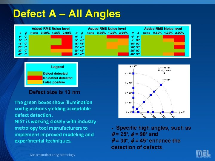 Defect A – All Angles Defect size is 13 nm The green boxes show illumination configurations yielding acceptable defect detection. NIST is working closely with industry metrology tool manufacturers to implement improved modeling and experimental techniques. Nanomanufacturing Metrology - Specific high angles, such as q = 25°, f = 90° and q = 30°, f = 45° enhance the detection of defects.
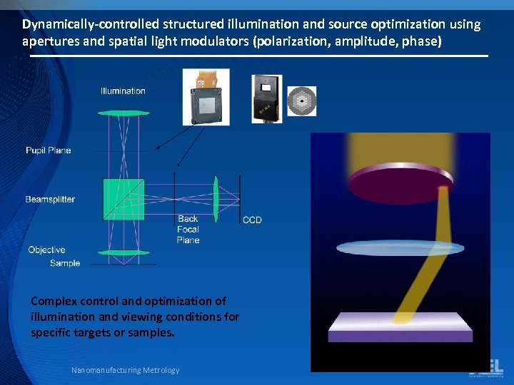 Dynamically-controlled structured illumination and source optimization using apertures and spatial light modulators (polarization, amplitude, phase) Complex control and optimization of illumination and viewing conditions for specific targets or samples. Nanomanufacturing Metrology
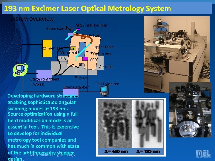 193 nm Excimer Laser Optical Metrology System SYSTEM OVERVIEW Beam combiner Align laser (visible) DUV fiber Upper table Excimer laser Motorized stage Optics box CCD PC Air table Stage controllers (7 -Axes) Stages Frame grabber Developing hardware strategies enabling sophisticated angular scanning modes at 193 nm. Source optimization using a full field modification mode is an essential tool. This is expensive to develop for individual metrology tool companies and has much in common with state of the art Nanomanufacturing Metrology lithography stepper design. CCD Monitor
 Conclusions • The simulation results demonstrate a range of defect types which can be measured better using polarization control, angle resolved illumination and wavelength optimization. • The scatterfield optical microscopy data and analysis compare favorably to conventional higher illumination numerical aperture imaging. • Spatial frequency modulation and source optimization of the illumination fields can be tailored to enhance specific content in the reflected fields. • The highly directional aspects of future lithography are well suited to modulated illumination fields. • MEL is playing an important role in developing and transferring measurement technology to targeted semiconductor metrology needs. • Industry funding and leadership in defining defect metrology challenges motivate a well directed, strong research effort to assist industry in maintaining device scaling goals necessary for future profitability. Nanomanufacturing Metrology


