e1ffe6f9bfa5dcb4b60eaac05e52ad54.ppt
- Количество слайдов: 21
 On May 4, 2011, Intel Corporation announced what it called the most radical shift in semiconductor technology in 50 years. A new 3 -dimensional transistor design will enable the production of integrated-circuit chips that operate faster with less power… The 3 -D Tri-Gate transistor is a variant of the Fin. FET developed at UC-Berkeley, and is being used in Intel’s 22 nmgeneration microprocessors.
 Lecture 24 OUTLINE The MOSFET (cont’d) • Advanced MOSFET structures Reading: Hu 7. 8
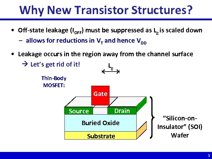 Why New Transistor Structures? • Off-state leakage (IOFF) must be suppressed as Lg is scaled down – allows for reductions in VT and hence VDD • Leakage occurs in the region away from the channel surface Let’s get rid of it! Lg Thin-Body MOSFET: Gate Source Drain Buried Oxide Substrate “Silicon-on. Insulator” (SOI) Wafer 3
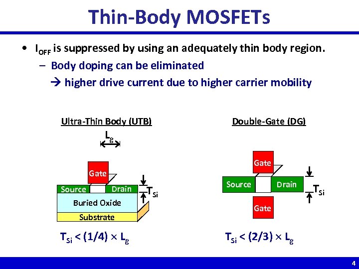 Thin-Body MOSFETs • IOFF is suppressed by using an adequately thin body region. – Body doping can be eliminated higher drive current due to higher carrier mobility Ultra-Thin Body (UTB) Lg Double-Gate (DG) Gate Source Drain Buried Oxide Substrate TSi < (1/4) Lg TSi Drain Source TSi Gate TSi < (2/3) Lg 4
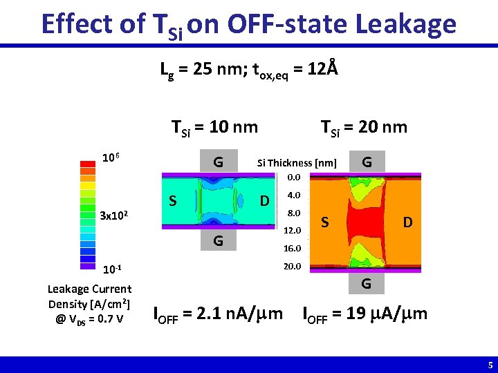 Effect of TSi on OFF-state Leakage Lg = 25 nm; tox, eq = 12Å TSi = 10 nm TSi = 20 nm G G 106 3 x 10² S Leakage Current Density [A/cm 2] @ VDS = 0. 7 V 0. 0 D G 10 -1 Si Thickness [nm] 4. 0 8. 0 12. 0 S D 16. 0 20. 0 G IOFF = 2. 1 n. A/ m IOFF = 19 A/ m 5
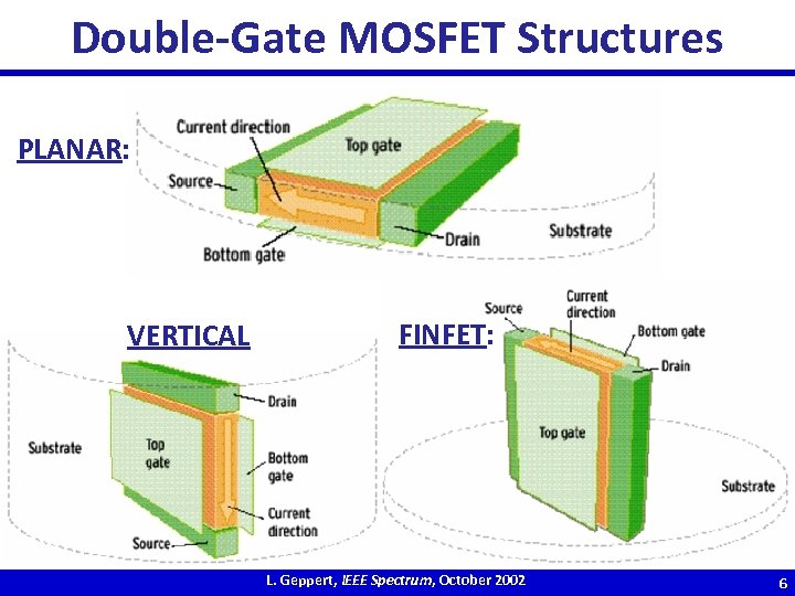 Double-Gate MOSFET Structures PLANAR: VERTICAL FINFET: L. Geppert, IEEE Spectrum, October 2002 6
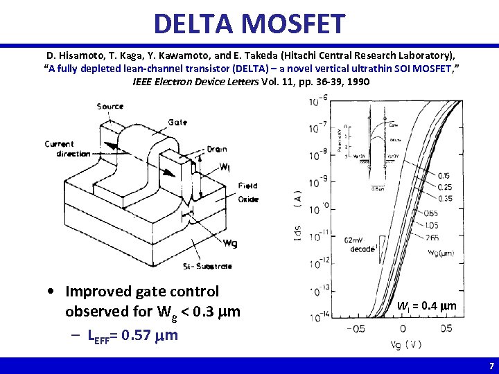 DELTA MOSFET D. Hisamoto, T. Kaga, Y. Kawamoto, and E. Takeda (Hitachi Central Research Laboratory), “A fully depleted lean-channel transistor (DELTA) – a novel vertical ultrathin SOI MOSFET, ” IEEE Electron Device Letters Vol. 11, pp. 36 -39, 1990 • Improved gate control observed for Wg < 0. 3 m – LEFF= 0. 57 m Wl = 0. 4 m 7
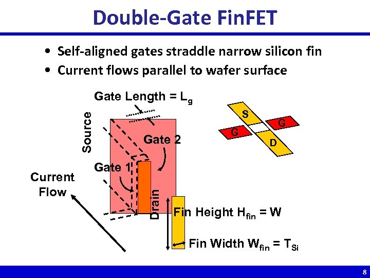 Double-Gate Fin. FET • Self-aligned gates straddle narrow silicon fin • Current flows parallel to wafer surface Gate Length = Lg Source S D Gate 1 Drain Current Flow Gate 2 G G Fin Height Hfin = W Fin Width Wfin = TSi 8
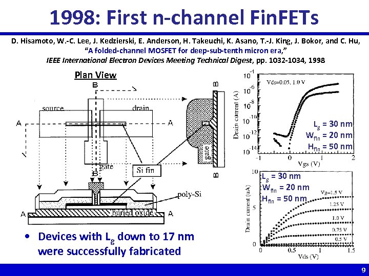 1998: First n-channel Fin. FETs D. Hisamoto, W. -C. Lee, J. Kedzierski, E. Anderson, H. Takeuchi, K. Asano, T. -J. King, J. Bokor, and C. Hu, “A folded-channel MOSFET for deep-sub-tenth micron era, ” IEEE International Electron Devices Meeting Technical Digest, pp. 1032 -1034, 1998 Plan View Lg = 30 nm Wfin = 20 nm Hfin = 50 nm • Devices with Lg down to 17 nm were successfully fabricated 9
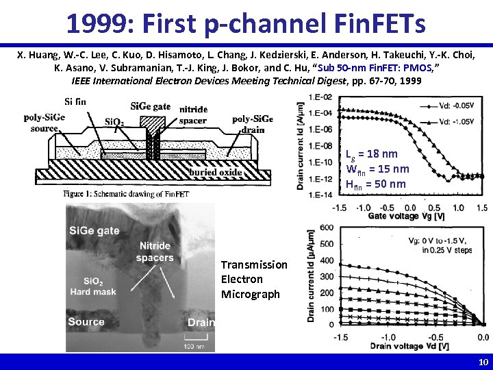 1999: First p-channel Fin. FETs X. Huang, W. -C. Lee, C. Kuo, D. Hisamoto, L. Chang, J. Kedzierski, E. Anderson, H. Takeuchi, Y. -K. Choi, K. Asano, V. Subramanian, T. -J. King, J. Bokor, and C. Hu, “Sub 50 -nm Fin. FET: PMOS, ” IEEE International Electron Devices Meeting Technical Digest, pp. 67 -70, 1999 Lg = 18 nm Wfin = 15 nm Hfin = 50 nm Transmission Electron Micrograph 10
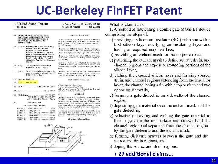 UC-Berkeley Fin. FET Patent + 27 additional claims… 11
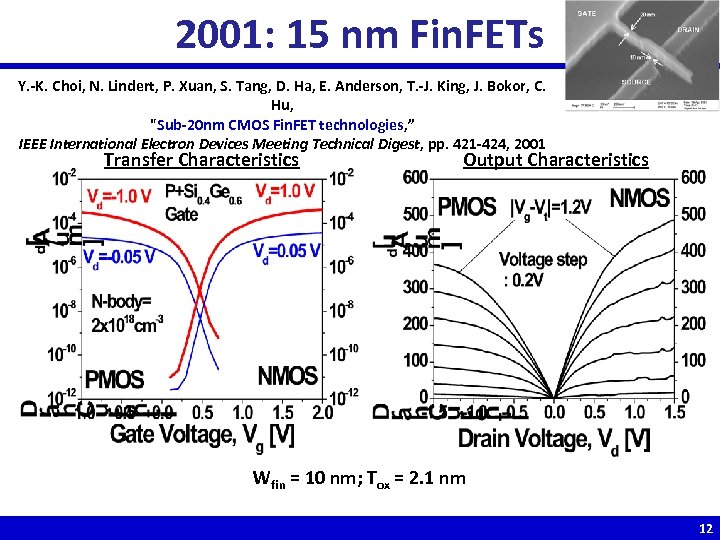 2001: 15 nm Fin. FETs Y. -K. Choi, N. Lindert, P. Xuan, S. Tang, D. Ha, E. Anderson, T. -J. King, J. Bokor, C. Hu, "Sub-20 nm CMOS Fin. FET technologies, ” IEEE International Electron Devices Meeting Technical Digest, pp. 421 -424, 2001 Transfer Characteristics Output Characteristics Wfin = 10 nm; Tox = 2. 1 nm 12
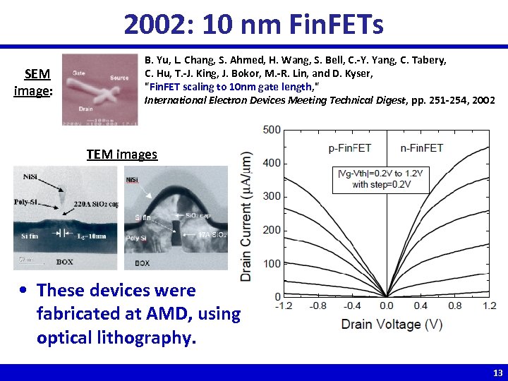 2002: 10 nm Fin. FETs SEM image: B. Yu, L. Chang, S. Ahmed, H. Wang, S. Bell, C. -Y. Yang, C. Tabery, C. Hu, T. -J. King, J. Bokor, M. -R. Lin, and D. Kyser, "Fin. FET scaling to 10 nm gate length, " International Electron Devices Meeting Technical Digest, pp. 251 -254, 2002 TEM images • These devices were fabricated at AMD, using optical lithography. 13
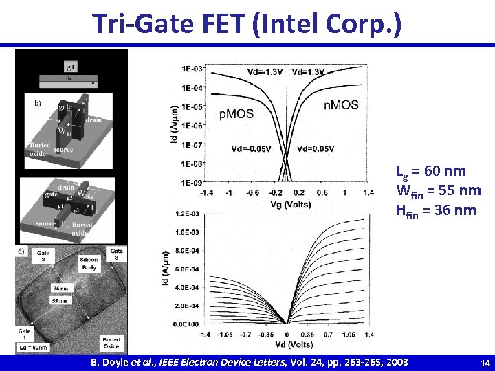 Tri-Gate FET (Intel Corp. ) Lg = 60 nm Wfin = 55 nm Hfin = 36 nm B. Doyle et al. , IEEE Electron Device Letters, Vol. 24, pp. 263 -265, 2003 14
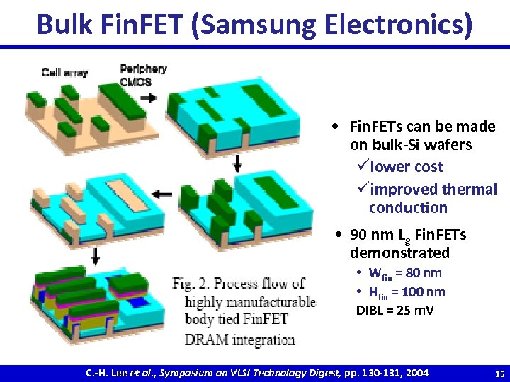 Bulk Fin. FET (Samsung Electronics) • Fin. FETs can be made on bulk-Si wafers ülower cost üimproved thermal conduction • 90 nm Lg Fin. FETs demonstrated • Wfin = 80 nm • Hfin = 100 nm DIBL = 25 m. V C. -H. Lee et al. , Symposium on VLSI Technology Digest, pp. 130 -131, 2004 15
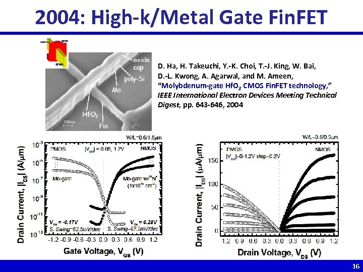 2004: High-k/Metal Gate Fin. FET D. Ha, H. Takeuchi, Y. -K. Choi, T. -J. King, W. Bai, D. -L. Kwong, A. Agarwal, and M. Ameen, “Molybdenum-gate Hf. O 2 CMOS Fin. FET technology, ” IEEE International Electron Devices Meeting Technical Digest, pp. 643 -646, 2004 16
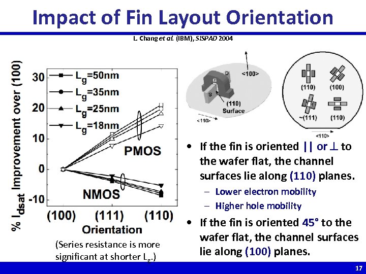 Impact of Fin Layout Orientation L. Chang et al. (IBM), SISPAD 2004 • If the fin is oriented || or to the wafer flat, the channel surfaces lie along (110) planes. – Lower electron mobility – Higher hole mobility (Series resistance is more significant at shorter Lg. ) • If the fin is oriented 45° to the wafer flat, the channel surfaces lie along (100) planes. 17
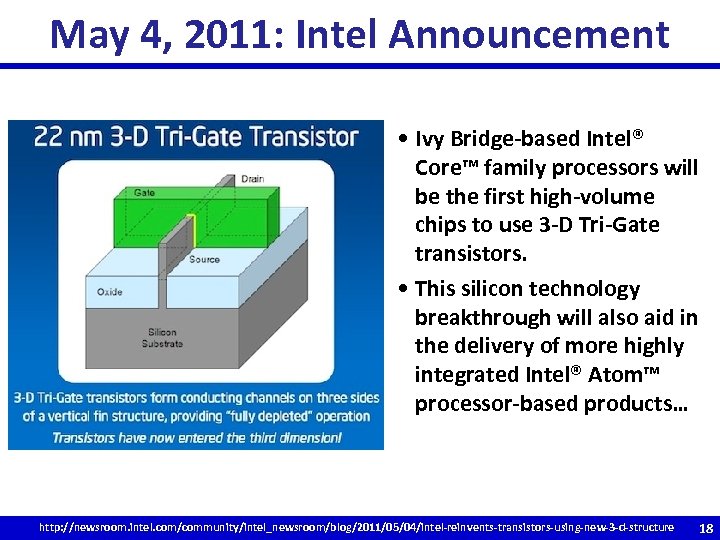 May 4, 2011: Intel Announcement • Ivy Bridge-based Intel® Core™ family processors will be the first high-volume chips to use 3 -D Tri-Gate transistors. • This silicon technology breakthrough will also aid in the delivery of more highly integrated Intel® Atom™ processor-based products… http: //newsroom. intel. com/community/intel_newsroom/blog/2011/05/04/intel-reinvents-transistors-using-new-3 -d-structure 18
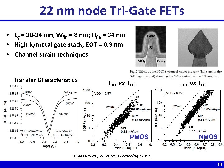 22 nm node Tri-Gate FETs • Lg = 30 -34 nm; Wfin = 8 nm; Hfin = 34 nm • High-k/metal gate stack, EOT = 0. 9 nm • Channel strain techniques Transfer Characteristics IOFF vs. IEFF PMOS IOFF vs. IEFF NMOS C. Auth et al. , Symp. VLSI Technology 2012 19
 National Science Foundation (NSF) Science and Technology Center (STC) for Energy Efficient Electronics Science Goal: Develop a new switch that can operate with VDD = 1 m. V PI: Eli Yablonovitch (UC Berkeley) 10 -yr project, started 15 Sep 2010 • Theme I: Nanoelectronics (Prof. Eli Yablonovitch) • Theme II: Nanomechanics (Prof. Tsu-Jae King Liu) • Theme III: Nanomagnetics (Prof. Jeffrey Bokor) • Theme IV: Nanophotonics (Prof. Ming Wu) Contra Costa-UC Berkeley-MIT-LATTC-Stanford-Tuskegee 20
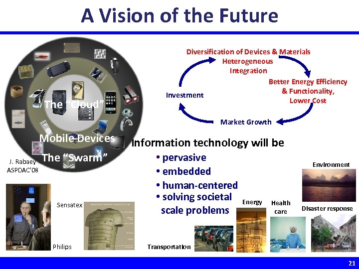 A Vision of the Future The “Cloud” Diversification of Devices & Materials Heterogeneous Integration Better Energy Efficiency & Functionality, Investment Lower Cost Market Growth Mobile Devices J. Rabaey ASPDAC’ 08 The “Swarm” Sensatex Philips Information technology will be • pervasive • embedded • human-centered • solving societal scale problems Environment Energy Health care Disaster response Transportation 21


