549738054b22c693ede1cc82eed742d3.ppt
- Количество слайдов: 74
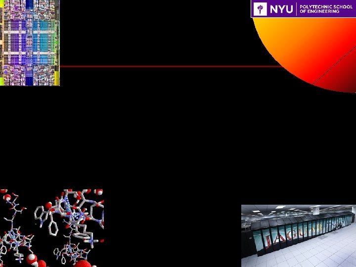
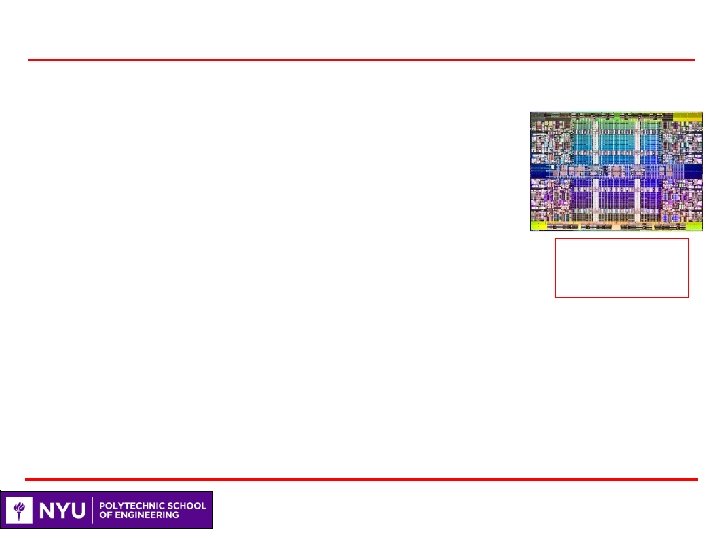


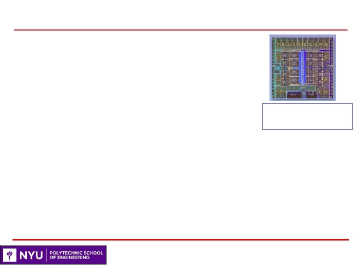


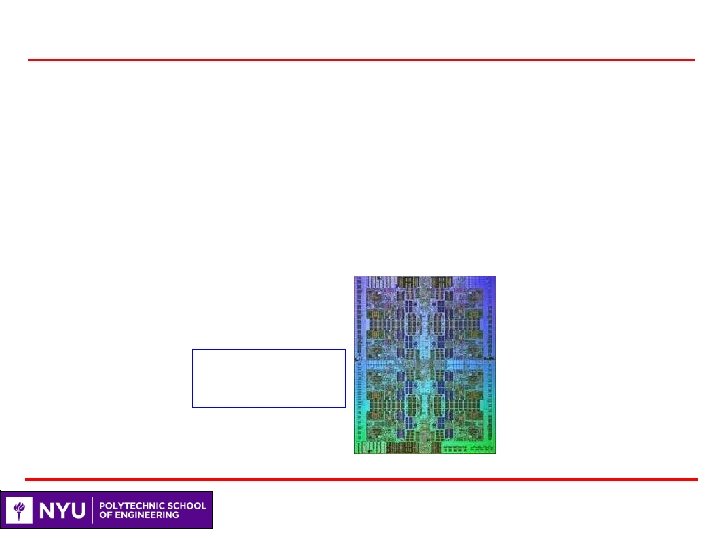
 NVIDIA TESLA GPU chip

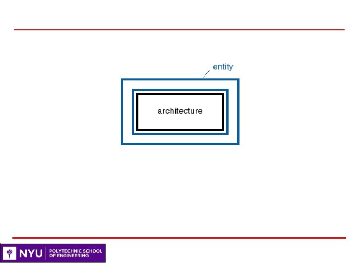
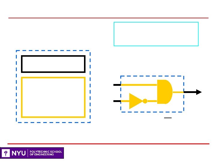
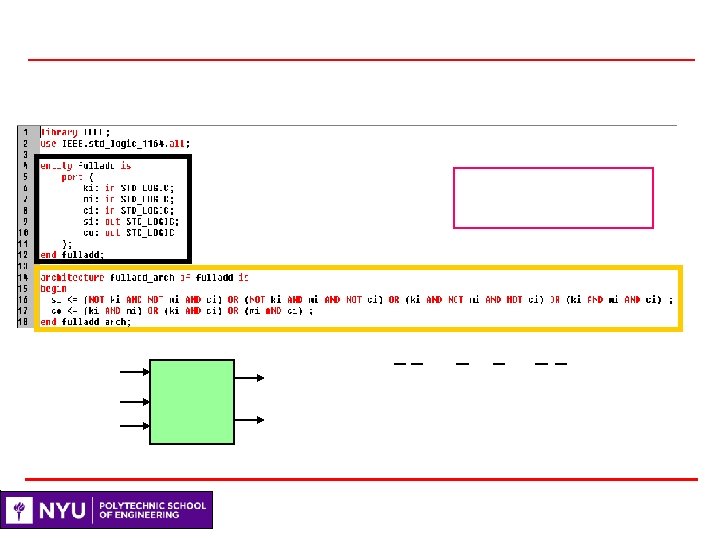
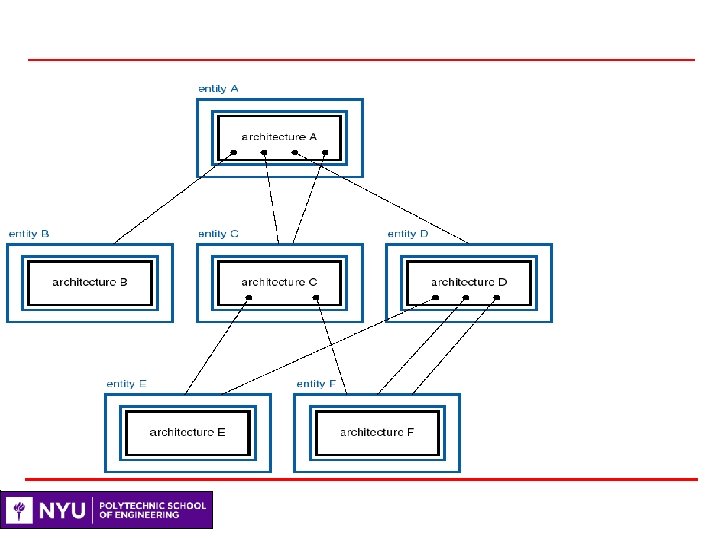
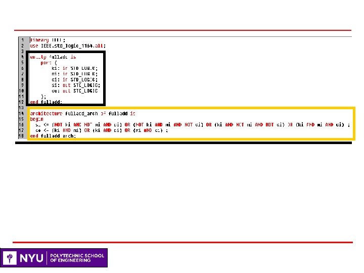
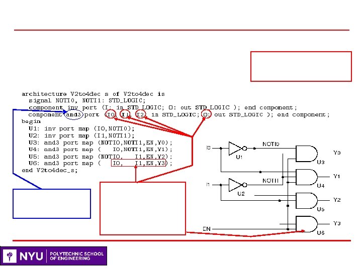
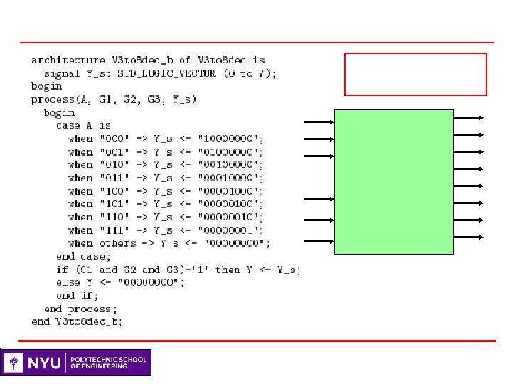
 Dataflow (less detailed) Behavioral (least detailed)") Structural (very detailed) Dataflow (less detailed) Behavioral (least detailed)
Structural (very detailed) Dataflow (less detailed) Behavioral (least detailed)
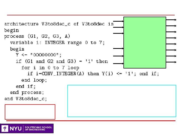
 Dataflow (less detailed) Behavioral (least detailed)") Structural (very detailed) Dataflow (less detailed) Behavioral (least detailed)
Structural (very detailed) Dataflow (less detailed) Behavioral (least detailed)


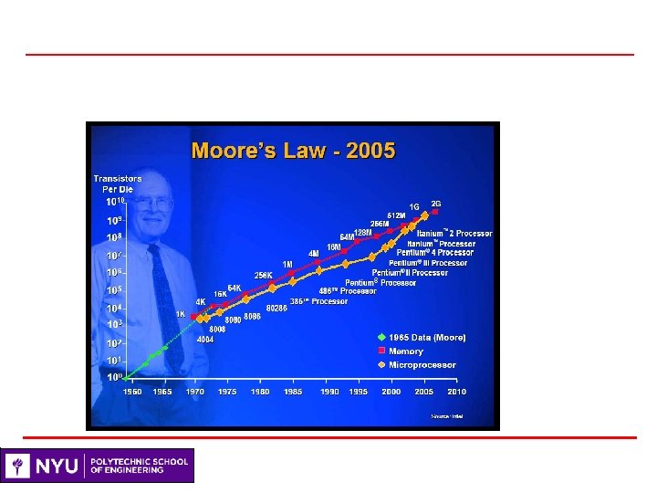
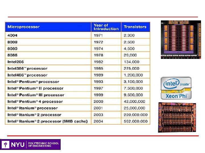
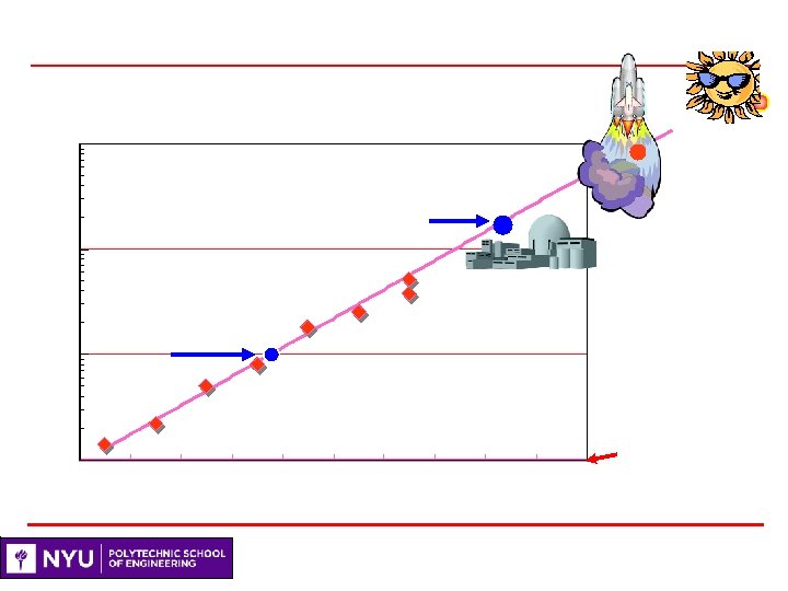
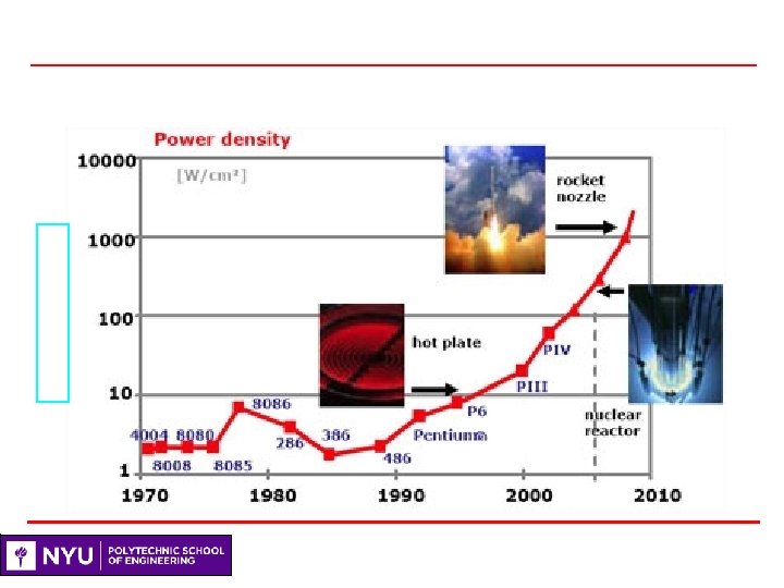
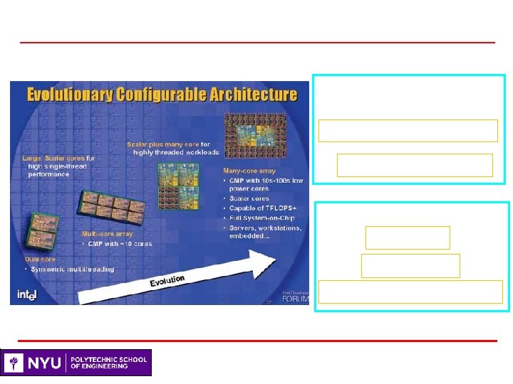
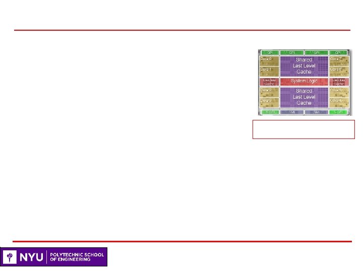
 Intel Technology Journal, November 2005


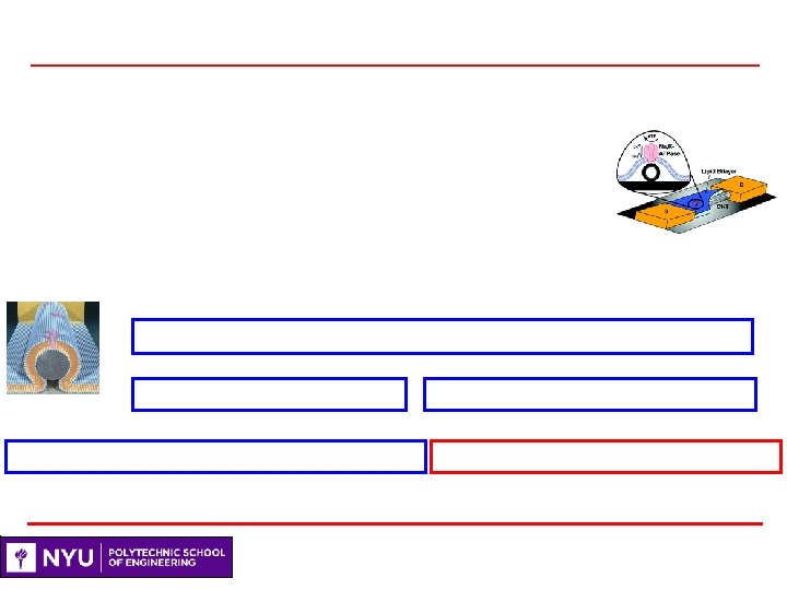
 A closer look at FPGA-like reconfigurable logic circuits Interface between CMOS and nanodevices Figures from : Konstantin K. Likharev A larger view of FPGA-like reconfigurable logic circuits Two CMOS cells and a nanodevice
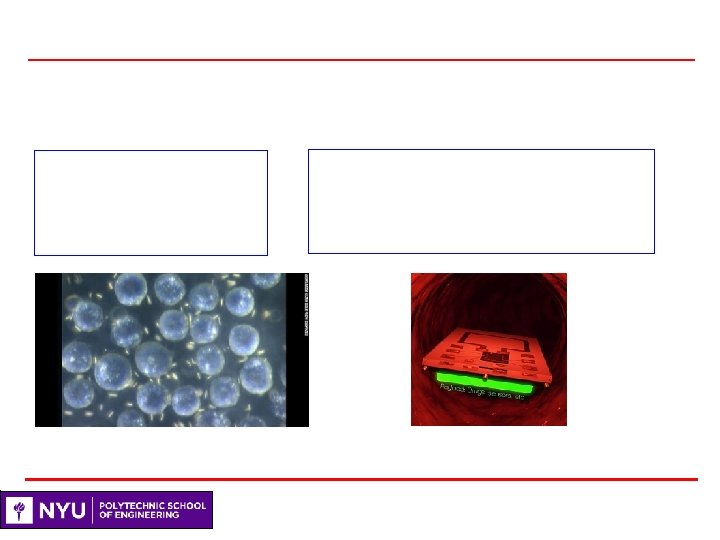
 UC Berkeley Sensor & Actuator Center
 Lung-on-a-chip : Harvard University
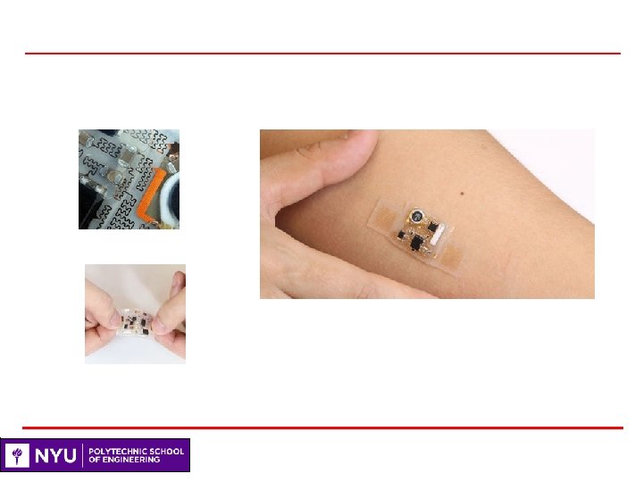
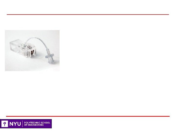
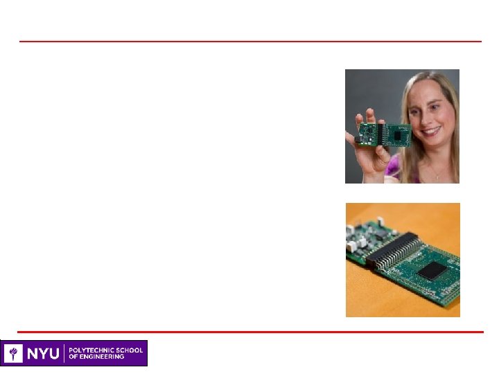
 Lab-on-a-chip sensors are ideal for use in rural clinics or at a patient’s bedside. But their widespread use for other tasks has long been stalled by seemingly insurmountable obstacles. For example, in wet environments—such as inside the body or outdoors—a chip’s metal conductors easily corrode or short, making the sensor unreliable. Many chips also contain materials such as arsenic that are toxic to humans. Their biggest drawback, though, is size. Today’s power sources, processors, and transmitters take up at least a few square centimeters—too big to squeeze through blood vessels. To overcome many of these problems, some researchers are seeking to replace a chip’s electronic circuits with optical ones. By using light rather than current to read chemical reactions, a photonic chip works reliably in aqueous solutions, is immune to electromagnetic radiation, tolerates a wide range of temperatures, and poses fewer risks to biological tissues.