8b93792a151082c6cfb4002938d6b961.ppt
- Количество слайдов: 38
Next Generation Optical Amplifiers requirements, bottlenecks, possible resolutions (Approach concerned on Cost, Footprint , Functionality rather than Efficiency, utilizing nano-photonics) Namkyoo Park Nanoscale Energy Conversion and Information Processing Devices September 24 th, 2006 Photonic Systems Laboratory School of EE, Seoul National University http: //stargate. snu. ac. kr nkpark@snu. ac. kr Photonic Systems Lab School of EECS, S. N. U.
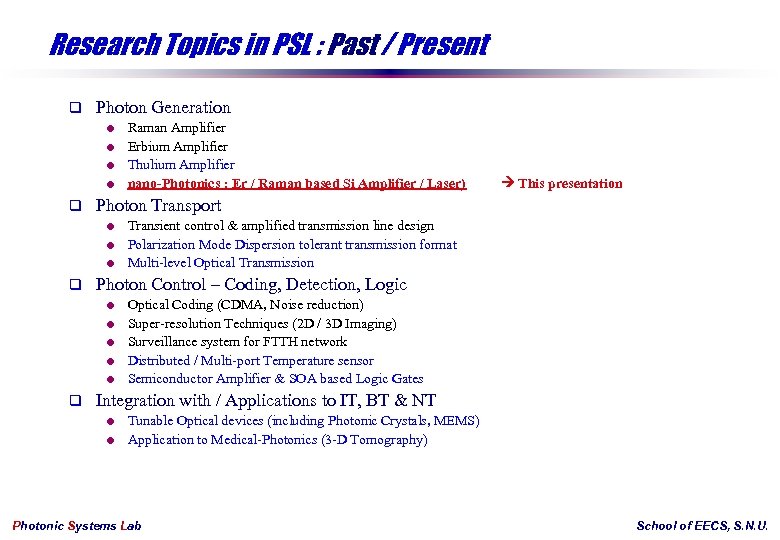
Research Topics in PSL : Past / Present q Photon Generation = Raman Amplifier = Erbium Amplifier = Thulium Amplifier = nano-Photonics : Er / Raman based Si Amplifier / Laser) q This presentation Photon Transport = Transient control & amplified transmission line design = Polarization Mode Dispersion tolerant transmission format = Multi-level Optical Transmission q Photon Control – Coding, Detection, Logic = Optical Coding (CDMA, Noise reduction) = Super-resolution Techniques (2 D / 3 D Imaging) = Surveillance system for FTTH network = Distributed / Multi-port Temperature sensor = Semiconductor Amplifier & SOA based Logic Gates q Integration with / Applications to IT, BT & NT = Tunable Optical devices (including Photonic Crystals, MEMS) = Application to Medical-Photonics (3 -D Tomography) Photonic Systems Lab School of EECS, S. N. U.
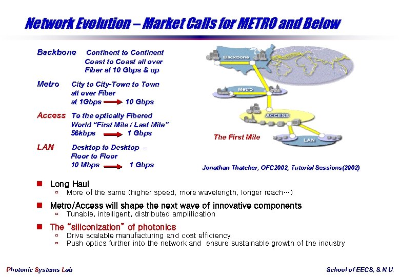
Network Evolution – Market Calls for METRO and Below Backbone Metro Continent to Continent Coast to Coast all over Fiber at 10 Gbps & up City to City-Town to Town all over Fiber at 1 Gbps 10 Gbps Access To the optically Fibered World “First Mile / Last Mile” 56 kbps 1 Gbps LAN Desktop to Desktop – Floor to Floor 10 Mbps 1 Gbps The First Mile Jonathan Thatcher, OFC 2002, Tutorial Sessions(2002) n Long Haul ù More of the same (higher speed, more wavelength, longer reach…) n Metro/Access will shape the next wave of innovative components ù Tunable, intelligent, distributed amplification n The “siliconization” of photonics ù ù Drive scalable manufacturing and cost efficiency Push optics further into the network and ensure sustainable growth of the industry Photonic Systems Lab School of EECS, S. N. U.
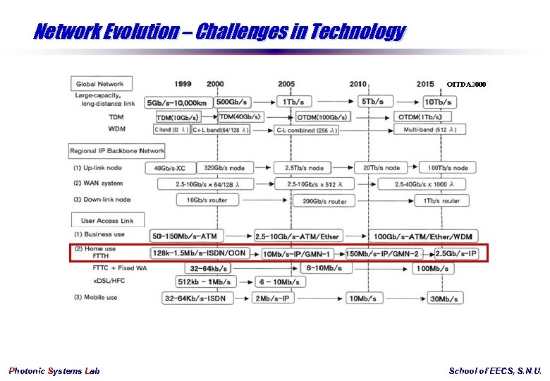
Network Evolution – Challenges in Technology OITDA 2000 Photonic Systems Lab School of EECS, S. N. U.
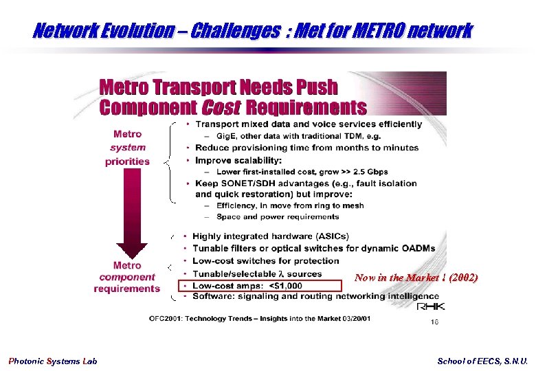
Network Evolution – Challenges : Met for METRO network Now in the Market ! (2002) Photonic Systems Lab School of EECS, S. N. U.
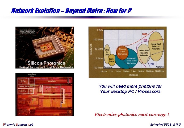
Network Evolution – Beyond Metro : How far ? You will need more photons for Your desktop PC / Processors Electronics-photonics must converge ! Photonic Systems Lab School of EECS, S. N. U.
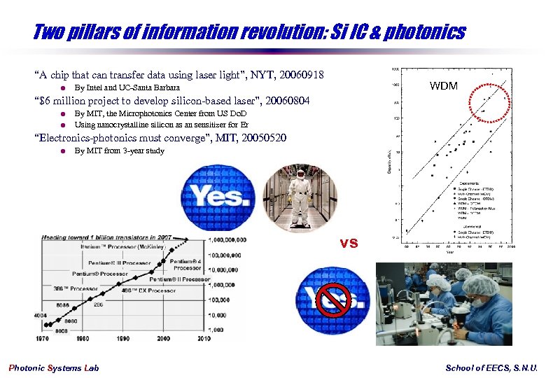
Two pillars of information revolution: Si IC & photonics “A chip that can transfer data using laser light”, NYT, 20060918 = WDM By Intel and UC-Santa Barbara “$6 million project to develop silicon-based laser”, 20060804 = = By MIT, the Microphotonics Center from US Do. D Using nanocrystalline silicon as an sensitizer for Er “Electronics-photonics must converge”, MIT, 20050520 = By MIT from 3 -year study vs Photonic Systems Lab School of EECS, S. N. U.
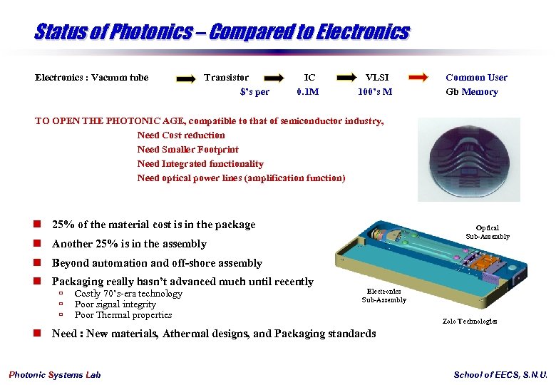
Status of Photonics – Compared to Electronics : Vacuum tube Transistor $’s per IC 0. 1 M VLSI 100’s M Common User Gb Memory TO OPEN THE PHOTONIC AGE, compatible to that of semiconductor industry, Need Cost reduction Need Smaller Footprint Need Integrated functionality Need optical power lines (amplification function) n 25% of the material cost is in the package Optical Sub-Assembly n Another 25% is in the assembly n Beyond automation and off-shore assembly n Packaging really hasn’t advanced much until recently ù ù ù Costly 70’s-era technology Poor signal integrity Poor Thermal properties Electronics Sub-Assembly Zolo Technologies n Need : New materials, Athermal designs, and Packaging standards Photonic Systems Lab School of EECS, S. N. U.
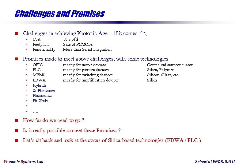
Challenges and Promises n Challenges in achieving Photonic Age -- if it comes ^^; ù ù ù n Cost Footprint Functionality 10’s of $ Size of PCMCIA More than Serial integration Promises made to meet above challenges, with some technologies ù ù ù ù ù OEIC PLC MEMS EDWA Hybrids Si-Photonics Plasmonics Ph-Xtals …. mostly for active devices mostly for passive devices mostly for switching devices mostly for amplification devices Compound semiconductor Silica, Polymer Silicon, Glass, etc. . Silica n How far do we need to go ? n Is it really possible to meet these Promises ? n Let’s sit back and look at the status of Silica based technologies (EDWA / PLC ) Photonic Systems Lab School of EECS, S. N. U.
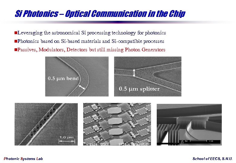
Si Photonics – Optical Communication in the Chip n. Leveraging n. Photonics n. Passives, the astronomical Si processing technology for photonics based on Si-based materials and Si-compatible processes Modulators, Detectors but still missing Photon Generators Photonic Systems Lab School of EECS, S. N. U.
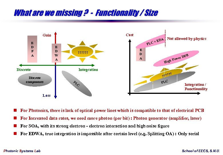
What are we missing ? - Functionality / Size Cost Gain E D F A A Not allowed by physics + ED PLC E D W A ? ? ? Discrete E D A wer h Po DFB Hig Integration Discrete components ? ? PL C ? ? PLC Integration / Functionality Loss n For Photonics, there is lack of optical power lines which is compatible to that of electrical PCB n For Increased data rates, we need more photon (per bit) : Photon generator (amplifier, laser) n For SOA, with its strong electron - electron interaction and high noise figure n For EDWA, true integration is impossible after certain level (e. g. Splitting OA) : Only serial Photonic Systems Lab School of EECS, S. N. U.
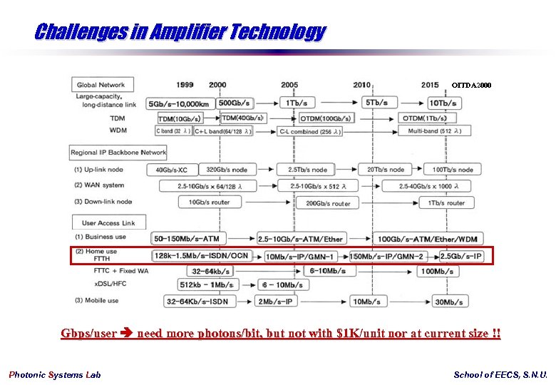
Challenges in Amplifier Technology OITDA 2000 Gbps/user need more photons/bit, but not with $1 K/unit nor at current size !! Photonic Systems Lab School of EECS, S. N. U.
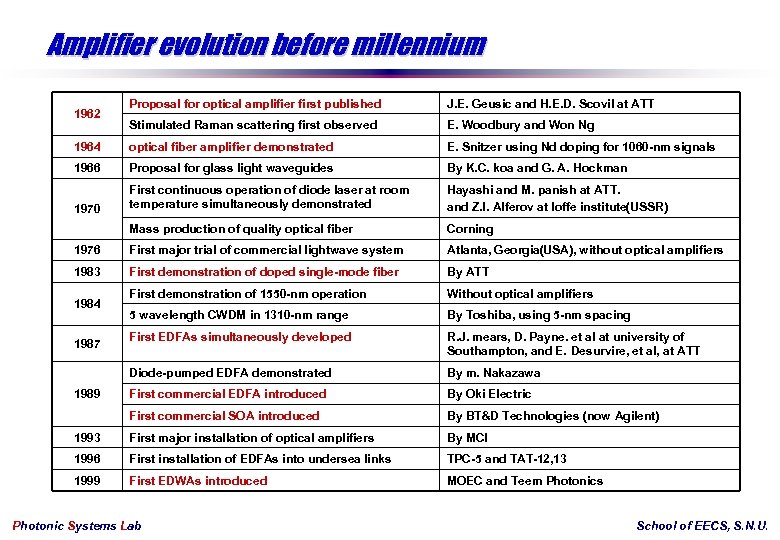
Amplifier evolution before millennium Proposal for optical amplifier first published J. E. Geusic and H. E. D. Scovil at ATT Stimulated Raman scattering first observed E. Woodbury and Won Ng 1964 optical fiber amplifier demonstrated E. Snitzer using Nd doping for 1060 -nm signals 1966 Proposal for glass light waveguides By K. C. koa and G. A. Hockman 1970 First continuous operation of diode laser at room temperature simultaneously demonstrated Hayashi and M. panish at ATT. and Z. I. Alferov at loffe institute(USSR) Mass production of quality optical fiber Corning 1976 First major trial of commercial lightwave system Atlanta, Georgia(USA), without optical amplifiers 1983 First demonstration of doped single-mode fiber By ATT First demonstration of 1550 -nm operation Without optical amplifiers 5 wavelength CWDM in 1310 -nm range By Toshiba, using 5 -nm spacing First EDFAs simultaneously developed R. J. mears, D. Payne. et al at university of Southampton, and E. Desurvire, et al, at ATT Diode-pumped EDFA demonstrated By m. Nakazawa First commercial EDFA introduced By Oki Electric First commercial SOA introduced By BT&D Technologies (now Agilent) 1993 First major installation of optical amplifiers By MCI 1996 First installation of EDFAs into undersea links TPC-5 and TAT-12, 13 1999 First EDWAs introduced MOEC and Teem Photonics 1962 1984 1987 1989 Photonic Systems Lab School of EECS, S. N. U.
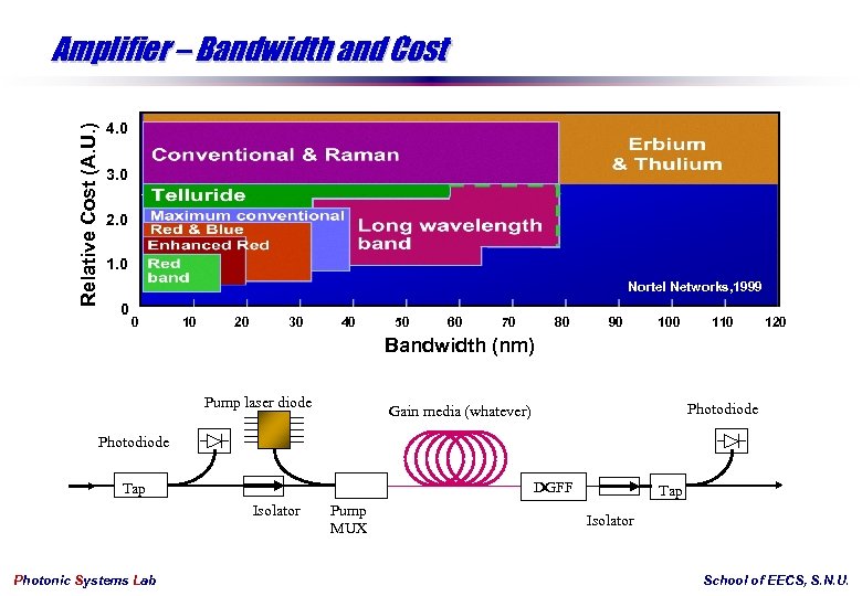
Relative Cost (A. U. ) Amplifier – Bandwidth and Cost 4. 0 3. 0 2. 0 1. 0 Nortel Networks, 1999 0 0 10 20 30 40 50 60 70 80 90 100 110 120 Bandwidth (nm) Pump laser diode Photodiode Gain media (whatever) Photodiode DGFF Tap Isolator Photonic Systems Lab Pump MUX Tap Isolator School of EECS, S. N. U.
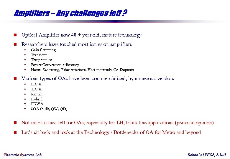
Amplifiers – Any challenges left ? n Optical Amplifier now 40 + year old, mature technology n Researchers have touched most issues on amplifiers ù ù ù n Gain flattening Transient Temperature Power Conversion efficiency Noise, Scattering, Fiber structure, Host materials, Co-Dopants Various types of OAs have been commercialized, by numerous vendors ù ù ù EDFA TDFA Raman Hybrid EDWA SOA (bulk, QW, QD) n Not much issues left for OAs, especially for LH, trunk line applications (personal opinion) n Let’s sit back and look at the Technology / Bottlenecks of OA for Metro and beyond Photonic Systems Lab School of EECS, S. N. U.
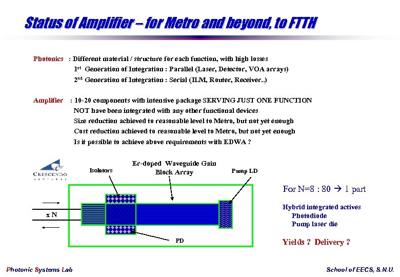
Status of Amplifier – for Metro and beyond, to FTTH Photonics : Different material / structure for each function, with high losses 1 st Generation of Integration : Parallel (Laser, Detector, VOA arrays) 2 nd Generation of Integration : Serial (ILM, Router, Receiver. . ) Amplifier : 10 -20 components with intensive package SERVING JUST ONE FUNCTION NOT have been integrated with any other functional devices Size reduction achieved to reasonable level to Metro, but not yet enough Cost reduction achieved to reasonable level to Metro, but not yet enough Is it possible to achieve above requirements with EDWA ? Isolators Er-doped Waveguide Gain Block Array Pump LD For N=8 : 80 1 part Hybrid integrated actives Photodiode Pump laser die x. N PD Photonic Systems Lab Yields ? Delivery ? School of EECS, S. N. U.
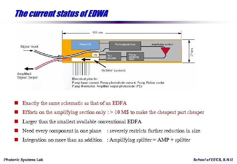
The current status of EDWA n Exactly the same schematic as that of an EDFA n Efforts on the amplifying section only : > 10 M$ to make the cheapest part cheaper n Larger than the smallest available conventional EDFA n Need every component in one plane : severely restricts further reduction in size n Integration no more than an addition : Amplifying splitter = AMP + splitter Photonic Systems Lab School of EECS, S. N. U.
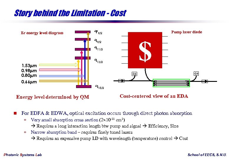
Story behind the Limitation - Cost Er energy level diagram 4 F 4 I Energy level determined by QM n 9/2 4 I 1. 53 m 0. 98 m 0. 80 m 0. 66 m Pump laser diode 9/2 11/2 4 I 13/2 4 I $ 15/2 Cost-centered view of an EDA For EDFA & EDWA, optical excitation occurs through direct photon absorption ù ù Very small absorption cross section (2 10 -21 cm 2) Requires a long interaction length btw pump and signal Efficiency, Size Narrow absorption band – requires finely tuned lasers Requires an expensive pump LD with wavelength (temperature) control Cost Photonic Systems Lab School of EECS, S. N. U.
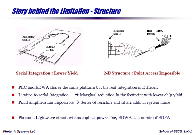
Story behind the Limitation - Structure Reflecting mirror Half MUX/ DMUX Amplifying Section Splitting Section Serial Integration : Lower Yield 2 -D Structure : Point Access Impossible n PLC and EDWA shares the same platform but the real integration is Difficult n Limited to serial integration n Point amplification impossible Series of resistors and filters adds in system noise n Photonic Lightwave circuit without optical power line, EDWA as a mimic of EDFA Photonic Systems Lab Marginal reduction in the footprint with lower chip yield School of EECS, S. N. U.
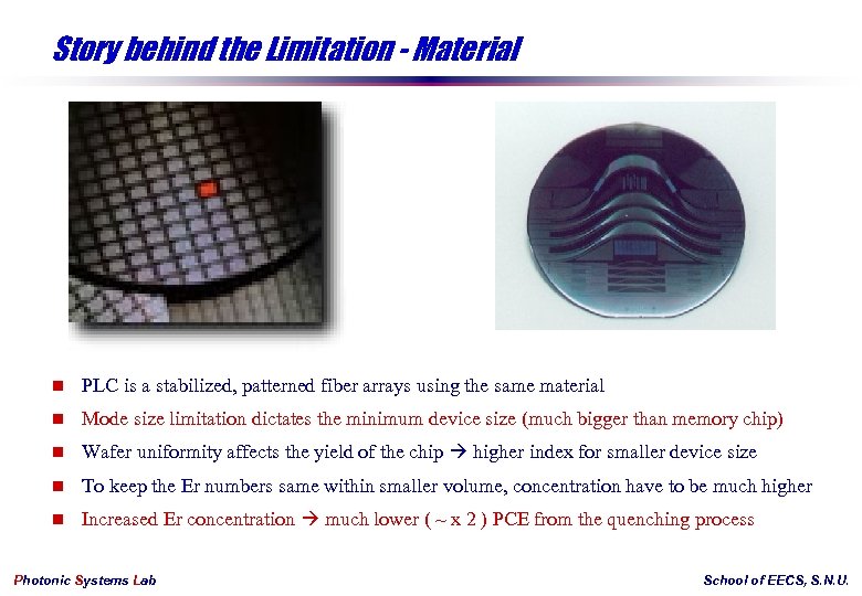
Story behind the Limitation - Material n PLC is a stabilized, patterned fiber arrays using the same material n Mode size limitation dictates the minimum device size (much bigger than memory chip) n Wafer uniformity affects the yield of the chip higher index for smaller device size n To keep the Er numbers same within smaller volume, concentration have to be much higher n Increased Er concentration much lower ( ~ x 2 ) PCE from the quenching process Photonic Systems Lab School of EECS, S. N. U.
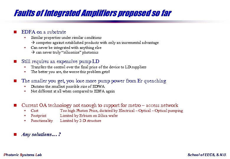
Faults of Integrated Amplifiers proposed so far n EDFA on a substrate ù ù n Still requires an expensive pump LD ù ù n Dictates the smallest possible size of EDWA Not different at all when compared to EDFA again Current OA technology not enough to support for metro – access network ù ù ù n Transfers the control over the final price of the device to LD suppliers The better you are, the worse this problem gets! The smaller you get, you lose more pump power from Er quenching ù ù n Similar properties under similar conditions competes against established products with only an incremental advantage Can never be integrated with anything else can never truly “siliconize” photonics Cost Footprint Functionality Too high Photon Price, dictated by Electrical – Optical pumping Limited by Erbium on Silica wafer Limited by 2 -D structure Any solutions… ? Photonic Systems Lab School of EECS, S. N. U.
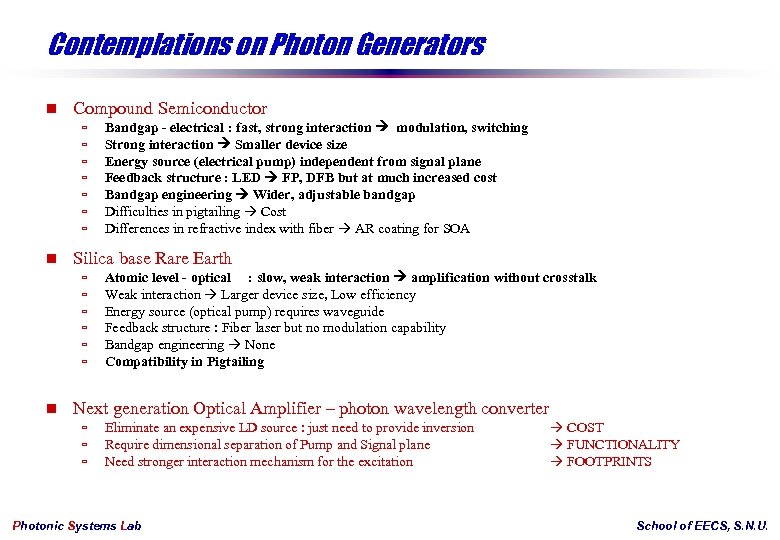
Contemplations on Photon Generators n Compound Semiconductor ù ù ù ù n Silica base Rare Earth ù ù ù n Bandgap - electrical : fast, strong interaction modulation, switching Strong interaction Smaller device size Energy source (electrical pump) independent from signal plane Feedback structure : LED FP, DFB but at much increased cost Bandgap engineering Wider, adjustable bandgap Difficulties in pigtailing Cost Differences in refractive index with fiber AR coating for SOA Atomic level - optical : slow, weak interaction amplification without crosstalk Weak interaction Larger device size, Low efficiency Energy source (optical pump) requires waveguide Feedback structure : Fiber laser but no modulation capability Bandgap engineering None Compatibility in Pigtailing Next generation Optical Amplifier – photon wavelength converter ù ù ù Eliminate an expensive LD source : just need to provide inversion Require dimensional separation of Pump and Signal plane Need stronger interaction mechanism for the excitation Photonic Systems Lab COST FUNCTIONALITY FOOTPRINTS School of EECS, S. N. U.
Si-Photonic Optical Amplifier ? Photonic Systems Lab School of EECS, S. N. U.
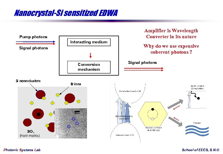
Nanocrystal-Si sensitized EDWA Amplifier is Wavelength Converter in its nature Pump photons Interacting medium Signal photons Conversion mechanism Si nanoclusters Why do we use expensive coherent photons ? Signal photons Er ions 20 nm Si. O 2 (host matrix) Photonic Systems Lab School of EECS, S. N. U.
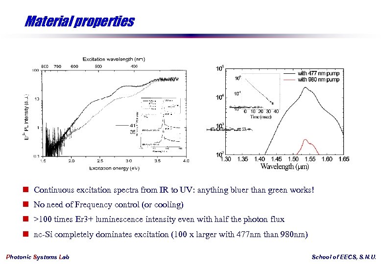
Material properties n Continuous excitation spectra from IR to UV: anything bluer than green works! n No need of Frequency control (or cooling) n >100 times Er 3+ luminescence intensity even with half the photon flux n nc-Si completely dominates excitation (100 x larger with 477 nm than 980 nm) Photonic Systems Lab School of EECS, S. N. U.
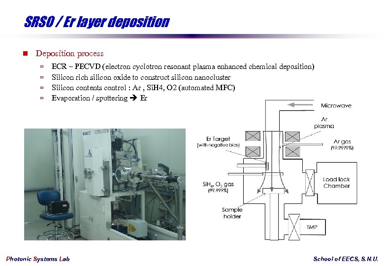
SRSO / Er layer deposition n Deposition process ù ù ECR – PECVD (electron cyclotron resonant plasma enhanced chemical deposition) Silicon rich silicon oxide to construct silicon nanocluster Silicon contents control : Ar , Si. H 4, O 2 (automated MFC) Evaporation / sputtering Er Photonic Systems Lab School of EECS, S. N. U.
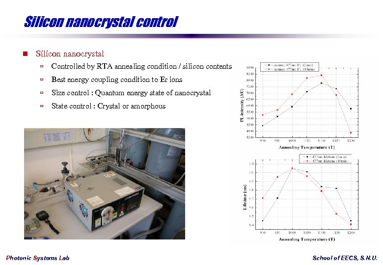
Silicon nanocrystal control n Silicon nanocrystal ù Controlled by RTA annealing condition / silicon contents ù Best energy coupling condition to Er ions ù Size control : Quantum energy state of nanocrystal ù State control : Crystal or amorphous Photonic Systems Lab School of EECS, S. N. U.
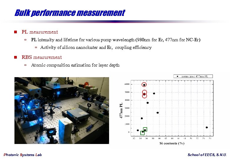
Bulk performance measurement n PL measurement ù PL intensity and lifetime for various pump wavelength (980 nm for Er, 477 nm for NC-Er) ù n Activity of silicon nanocluster and Er, coupling efficiency RBS measurement ù Atomic composition estimation for layer depth Photonic Systems Lab School of EECS, S. N. U.
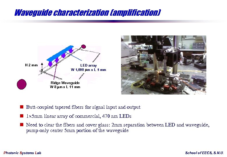
Waveguide characterization (amplification) H 2 mm LED array W 1, 000 m x L 5 mm Ridge Waveguide W 8 m x L 11 mm n Butt-coupled tapered fibers for signal input and output n 1 5 mm linear array of commercial, 470 nm LEDs n Need to clear the fibers and cover glass: 2 mm separation between LED and waveguide, pump only center 5 mm portion of the waveguide Photonic Systems Lab School of EECS, S. N. U.
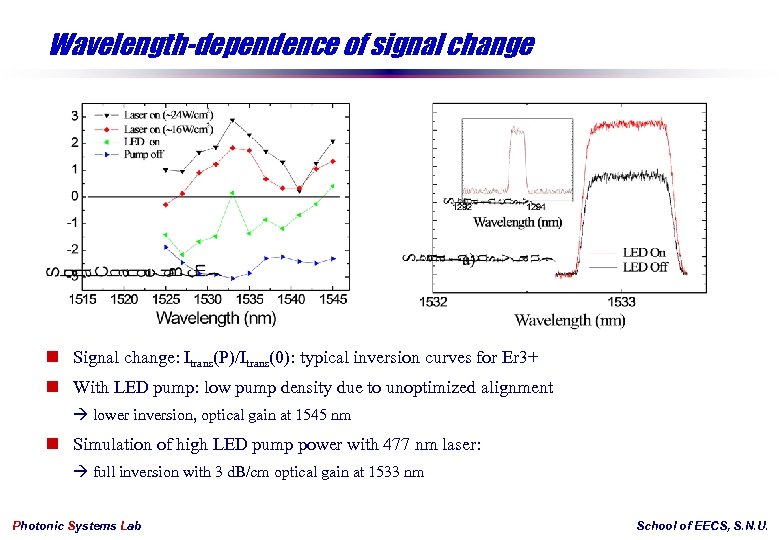
Wavelength-dependence of signal change n Signal change: Itrans(P)/Itrans(0): typical inversion curves for Er 3+ n With LED pump: low pump density due to unoptimized alignment lower inversion, optical gain at 1545 nm n Simulation of high LED pump power with 477 nm laser: full inversion with 3 d. B/cm optical gain at 1533 nm Photonic Systems Lab School of EECS, S. N. U.
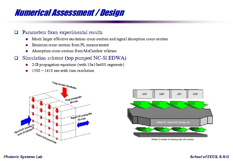
Numerical Assessment / Design q Parameters from experimental results = Much larger effective excitation cross-section and signal absorption cross-section = Emission cross-section from PL measurement = Absorption cross-section from Mc. Cumber relation q Simulation scheme (top pumped NC-Si EDWA) = 2 -D propagation equations (with 10 x 400 segments) = 1500 ~ 1610 nm with 1 nm resolution Photonic Systems Lab School of EECS, S. N. U.
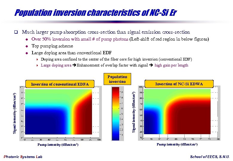
Population inversion characteristics of NC-Si Er q Much larger pump absorption cross-section than signal emission cross-section Over 50% inversion with small # of pump photons (Left-shift of red region in below figures) = Top pumping scheme = Large doping area than conventional EDF = 4 Doping area confined to the center of the fiber core for high inversion (conventional EDF) 4 Large doping area Enhancement of overlap factor with signal high gain per length Inversion of NC-Si EDWA Signal intensity (d. Bm/cm 2) Inversion of conventional EDFA Population inversion Pump intensity (d. Bm/cm 2) Photonic Systems Lab Pump intensity (d. Bm/cm 2) School of EECS, S. N. U.
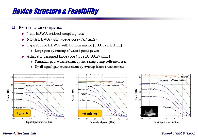
Device Structure & Feasibility q Performance comparison 4 cm EDWA without coupling loss = NC-Si EDWA with type A core (7 x 7 μm 2) = Type A core EDWA with bottom mirror (100% reflection) = 4 Large gain by reusing of wasted pump power = Adiabatic designed large core (type B, 100 x 7 μm 2) 4 Saturation gain enhancement by increasing pump collection area 4 Small signal gain enhancement by overlap factor enhancement Type A Photonic Systems Lab w/ mirror School of EECS, S. N. U.
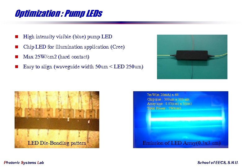
Optimization : Pump LEDs n High intensity visible (blue) pump LED n Chip LED for illumination application (Cree) n Max 25 W/cm 2 (hard contact) n Easy to align (waveguide width 50 um < LED 250 um) 7 m. W(at 20 m. A) x 64 Chip size : 300 um x 300 um Array size : 0. 03(cm) x 3(cm) Total Power : 5 W/cm 2 LED Die-Bonding pattern Photonic Systems Lab Emission of LED Array(0. 3 x 3 cm) School of EECS, S. N. U.
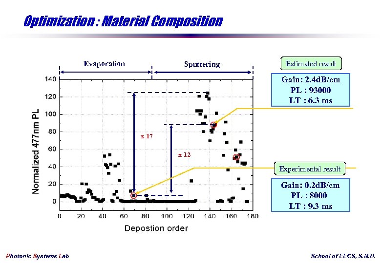
Optimization : Material Composition Evaporation Sputtering Estimated result Gain: 2. 4 d. B/cm PL : 93000 LT : 6. 3 ms x 17 x 12 Experimental result Gain: 0. 2 d. B/cm PL : 8000 LT : 9. 3 ms Photonic Systems Lab School of EECS, S. N. U.
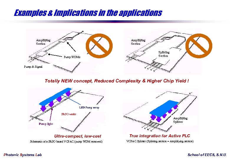
Examples & Implications in the applications Amplifying Section Pump WDMs Splitting Section Pump & Signal Totally NEW concept, Reduced Complexity & Higher Chip Yield ! LED Pump array SRSO wafer Amplifying Splitter Pump light Ultra-compact, low-cost Schematic of a SRSO based VCPAC (pump WDM removed) Photonic Systems Lab True integration for Active PLC VCPAC Splitter (Splitting section = Amplifying section) School of EECS, S. N. U.
Summary Much things you can do with NANO Si !! That’s a good news for Photonics Engineers # of Amplifier Worldwide # of nano-particle Worldwide # of Amplifier Engineers Photonic Systems Lab School of EECS, S. N. U.

Photonic Systems Lab School of EECS, S. N. U.
8b93792a151082c6cfb4002938d6b961.ppt