a18112e1d1b073d60c1341b49a19c1d2.ppt
- Количество слайдов: 57
 New England Lead Free Electronics Consortium Greg Morose Toxics Use Reduction Institute University of Massachusetts Lowell 1
 Agenda • Consortium Overview • Phase III Process • Phase III Results and Conclusions • Next Steps 2
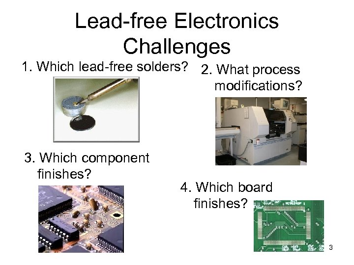 Lead-free Electronics Challenges 1. Which lead-free solders? 2. What process modifications? 3. Which component finishes? 4. Which board finishes? 3
 New England Lead-free Electronics Consortium Government Funding Project Mngmt. Outreach Academia Pull testing Statistical analysis Industry Components Equipment Technical expertise 4
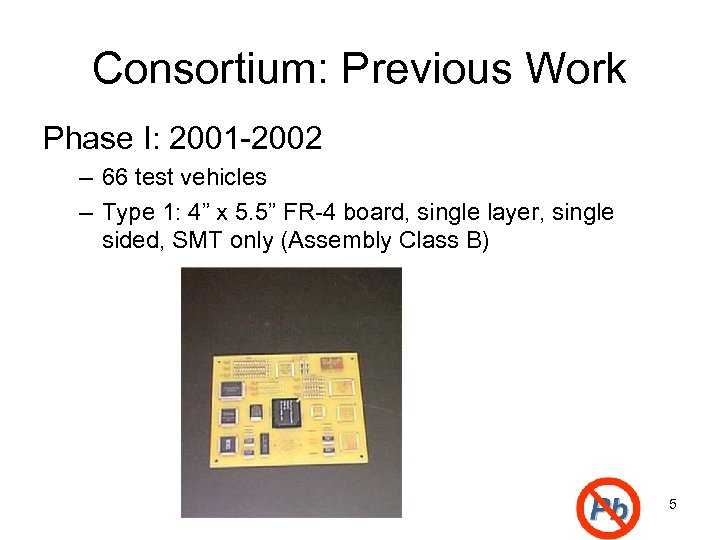 Consortium: Previous Work Phase I: 2001 -2002 – 66 test vehicles – Type 1: 4” x 5. 5” FR-4 board, single layer, single sided, SMT only (Assembly Class B) 5
 Phase I – Parameters • Solder Alloys • Sn/Ag/Cu(95. 5/3. 8/0. 7) • Sn/Ag (96. 5/3. 5) • Sn/Bi (57/43) • PWB Surface Finishes • OSP (Organic Solder Protectants) • Electroless Nickel Immersion Gold (ENIG) • Thermal Profiles • Soak with 60 sec, 90 sec, 120 sec above liquidus • Linear with 60 sec, 90 sec, 120 sec above liquidus temp. • Reflow Environment • Nitrogen vs. Air reflow 6
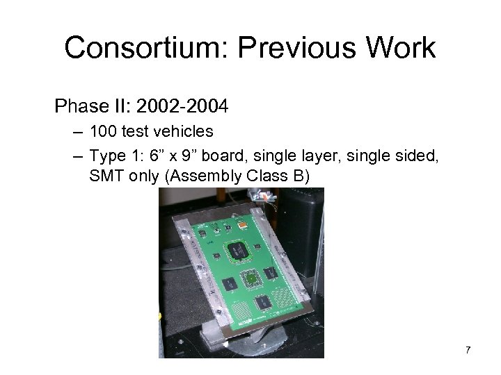 Consortium: Previous Work Phase II: 2002 -2004 – 100 test vehicles – Type 1: 6” x 9” board, single layer, single sided, SMT only (Assembly Class B) 7
 Phase II – Parameters 1. PWB Finishes – Solder Mask Over Bare Copper with Hot Air Solder Leveling (SMOBC/HASL), Matte Tin (Sn), Immersion Silver (Ag), Organic Solder Preservative (OSP), and Electroless Nickel Immersion Gold (ENIG). 2. Reflow Atmospheres – Two Treatments – Air and Nitrogen. 3. Solder Pastes – 95. 5 Sn-3. 8 Ag-0. 7 Cu alloy from three different suppliers (A, B and C), all incorporating no-clean fluxes. 4. Component Lead Finishes – matte tin, tin/silver/copper, nickel/palladium/gold, and nickel/gold. Sn-Pb eutectic solder PWB using the solder treatments as control PWBs. 8
 Phase III • Implementation not experimentation, test vehicle simulates production board • Focus on solder joint integrity • Funding: U. S. EPA 9
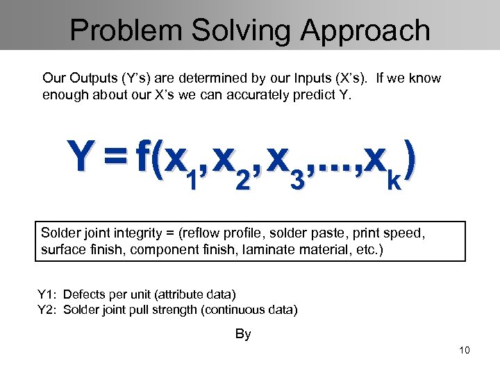 Problem Solving Approach Our Outputs (Y’s) are determined by our Inputs (X’s). If we know enough about our X’s we can accurately predict Y. Y = f(x 1, x 2, x 3, . . . , xk ) Solder joint integrity = (reflow profile, solder paste, print speed, surface finish, component finish, laminate material, etc. ) Y 1: Defects per unit (attribute data) Y 2: Solder joint pull strength (continuous data) By 10
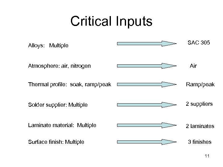 Critical Inputs Alloys: Multiple Atmosphere: air, nitrogen SAC 305 Air Thermal profile: soak, ramp/peak Ramp/peak Solder supplier: Multiple 2 suppliers Laminate material: Multiple 2 laminates Surface finish: Multiple 3 finishes 11
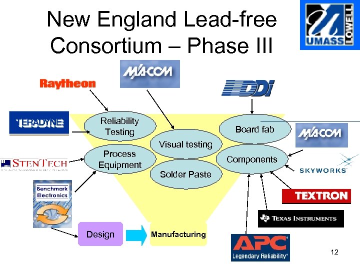 New England Lead-free Consortium – Phase III Reliability Testing Process Equipment Design Board fab Visual testing Components Solder Paste Manufacturing 12
 Phase III Process 13
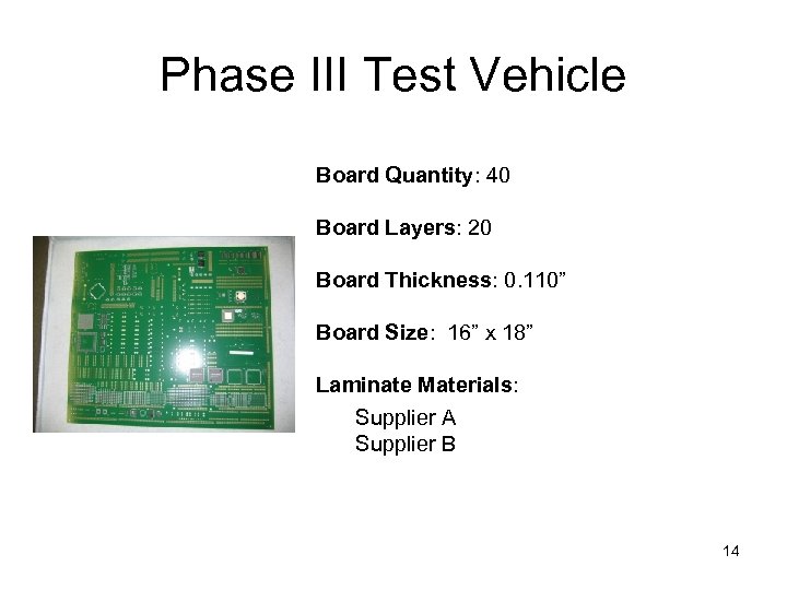 Phase III Test Vehicle Board Quantity: 40 Board Layers: 20 Board Thickness: 0. 110” Board Size: 16” x 18” Laminate Materials: Supplier A Supplier B 14
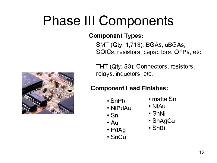 Phase III Components Component Types: SMT (Qty: 1, 713): BGAs, u. BGAs, SOICs, resistors, capacitors, QFPs, etc. THT (Qty: 53): Connectors, resistors, relays, inductors, etc. Component Lead Finishes: • Sn. Pb • Ni. Pd. Au • Sn • Au • Pd. Ag • Sn. Cu • matte Sn • Ni. Au • Sn. Ni • Sn. Ag. Cu • Sn. Bi 15
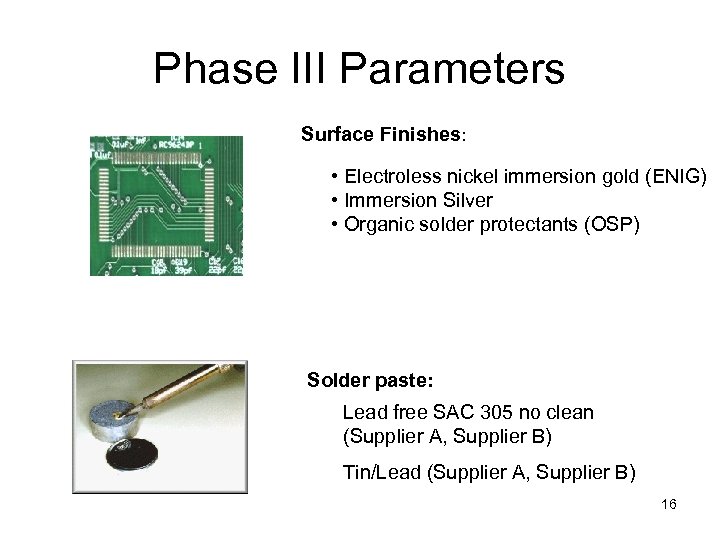 Phase III Parameters Surface Finishes: • Electroless nickel immersion gold (ENIG) • Immersion Silver • Organic solder protectants (OSP) Solder paste: Lead free SAC 305 no clean (Supplier A, Supplier B) Tin/Lead (Supplier A, Supplier B) 16
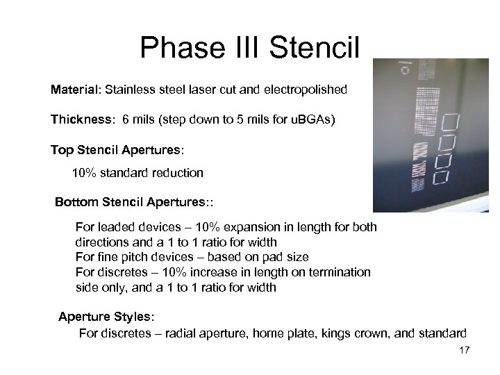 Phase III Stencil Material: Stainless steel laser cut and electropolished Thickness: 6 mils (step down to 5 mils for u. BGAs) Top Stencil Apertures: 10% standard reduction Bottom Stencil Apertures: : For leaded devices – 10% expansion in length for both directions and a 1 to 1 ratio for width For fine pitch devices – based on pad size For discretes – 10% increase in length on termination side only, and a 1 to 1 ratio for width Aperture Styles: For discretes – radial aperture, home plate, kings crown, and standard 17
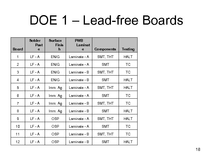 DOE 1 – Lead-free Boards Board Solder Past e Surface Finis h PWB Laminat e Components Testing 1 LF - A ENIG Laminate - A SMT, THT HALT 2 LF - A ENIG Laminate - A SMT TC 3 LF - A ENIG Laminate - B SMT, THT TC 4 LF - A ENIG Laminate - B SMT HALT 5 LF - A Imm. Ag Laminate - A SMT, THT HALT 6 LF - A Imm. Ag Laminate - A SMT TC 7 LF - A Imm. Ag Laminate - B SMT, THT TC 8 LF - A Imm. Ag Laminate - B SMT HALT 9 LF - A OSP Laminate - A SMT, THT HALT 10 LF - A OSP Laminate - A SMT TC 11 LF - A OSP Laminate - B SMT, THT TC 12 LF - A OSP Laminate - B SMT HALT 18
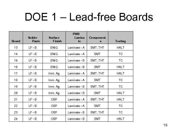 DOE 1 – Lead-free Boards Board Solder Paste Surface Finish PWB Lamina te Component s Testing 13 LF - B ENIG Laminate - A SMT, THT HALT 14 LF - B ENIG Laminate - A SMT TC 15 LF - B ENIG Laminate - B SMT, THT TC 16 LF - B ENIG Laminate - B SMT HALT 17 LF - B Imm. Ag Laminate - A SMT, THT HALT 18 LF - B Imm. Ag Laminate - A SMT TC 19 LF - B Imm. Ag Laminate - B SMT, THT TC 20 LF - B Imm. Ag Laminate - B SMT HALT 21 LF - B OSP Laminate - A SMT, THT HALT 22 LF - B OSP Laminate - A SMT TC 23 LF - B OSP Laminate - B SMT, THT TC 24 LF - B OSP Laminate - B SMT HALT 19
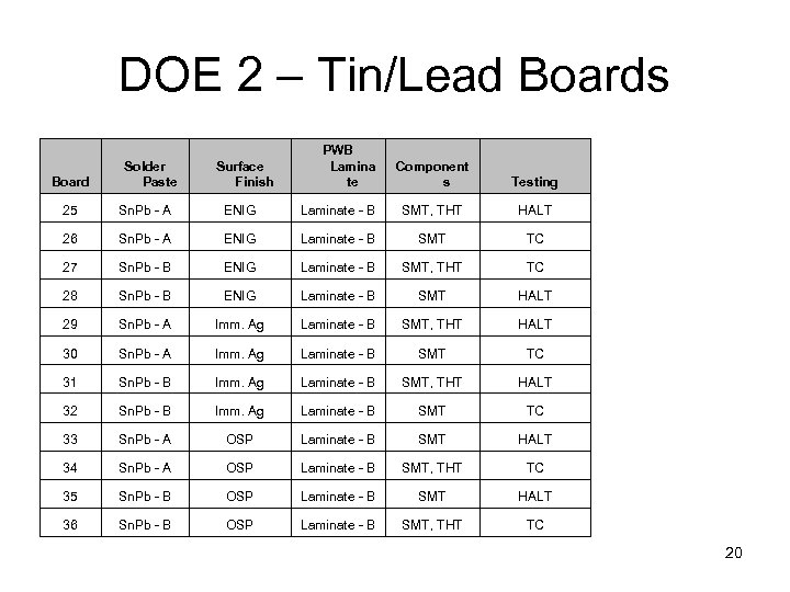 DOE 2 – Tin/Lead Boards Board Solder Paste Surface Finish PWB Lamina te Component s Testing 25 Sn. Pb - A ENIG Laminate - B SMT, THT HALT 26 Sn. Pb - A ENIG Laminate - B SMT TC 27 Sn. Pb - B ENIG Laminate - B SMT, THT TC 28 Sn. Pb - B ENIG Laminate - B SMT HALT 29 Sn. Pb - A Imm. Ag Laminate - B SMT, THT HALT 30 Sn. Pb - A Imm. Ag Laminate - B SMT TC 31 Sn. Pb - B Imm. Ag Laminate - B SMT, THT HALT 32 Sn. Pb - B Imm. Ag Laminate - B SMT TC 33 Sn. Pb - A OSP Laminate - B SMT HALT 34 Sn. Pb - A OSP Laminate - B SMT, THT TC 35 Sn. Pb - B OSP Laminate - B SMT HALT 36 Sn. Pb - B OSP Laminate - B SMT, THT TC 20
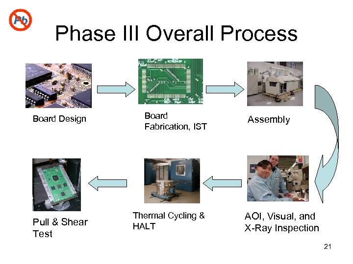 Phase III Overall Process Board Design Pull & Shear Test Board Fabrication, IST Thermal Cycling & HALT Assembly AOI, Visual, and X-Ray Inspection 21
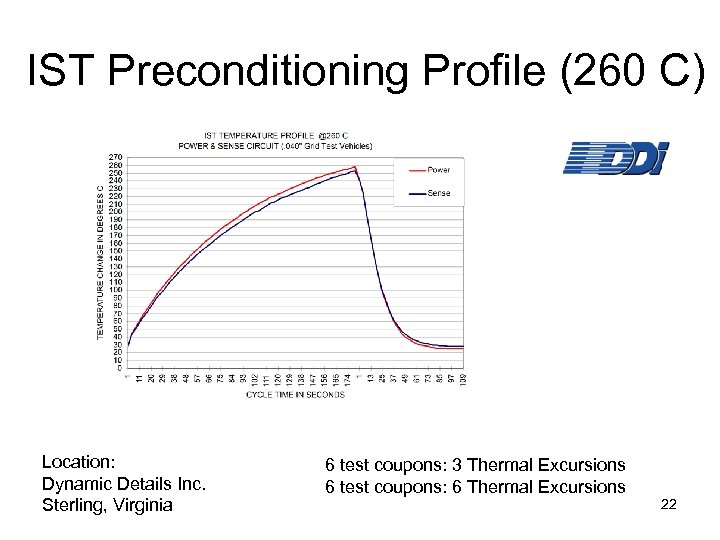 IST Preconditioning Profile (260 C) Location: Dynamic Details Inc. Sterling, Virginia 6 test coupons: 3 Thermal Excursions 6 test coupons: 6 Thermal Excursions 22
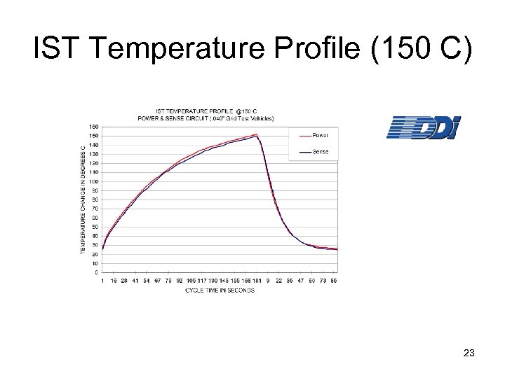 IST Temperature Profile (150 C) 23
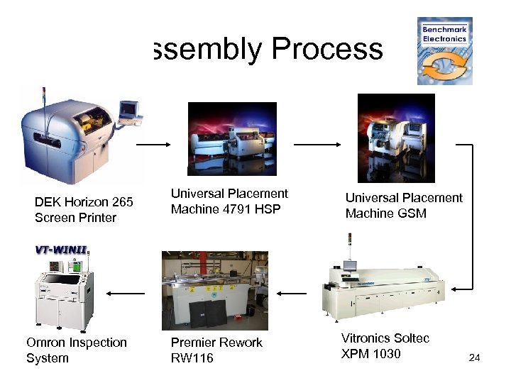 Assembly Process DEK Horizon 265 Screen Printer Omron Inspection System Universal Placement Machine 4791 HSP Premier Rework RW 116 Universal Placement Machine GSM Vitronics Soltec XPM 1030 24
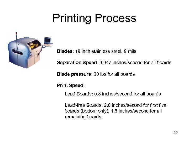 Printing Process Blades: 19 inch stainless steel, 9 mils Separation Speed: 0. 047 inches/second for all boards Blade pressure: 30 lbs for all boards Print Speed: Lead Boards: 0. 8 inches/second for all boards Lead-free Boards: 2. 0 inches/second for first five boards (bottom only), 1. 5 inches/second for all remaining boards 25
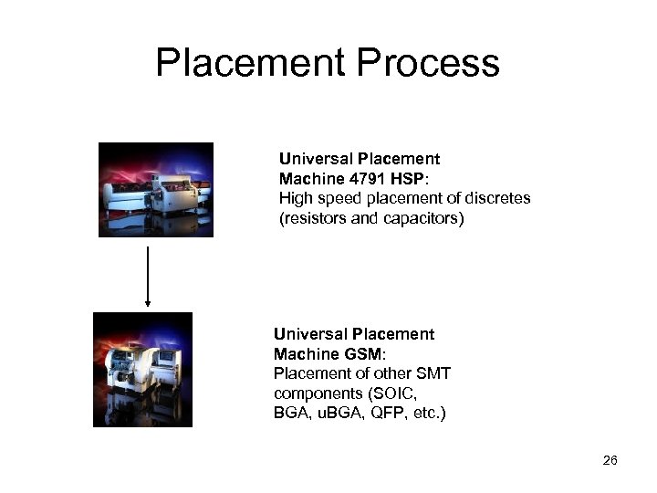 Placement Process Universal Placement Machine 4791 HSP: High speed placement of discretes (resistors and capacitors) Universal Placement Machine GSM: Placement of other SMT components (SOIC, BGA, u. BGA, QFP, etc. ) 26
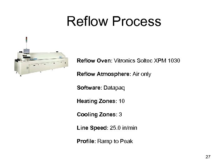 Reflow Process Reflow Oven: Vitronics Soltec XPM 1030 Reflow Atmosphere: Air only Software: Datapaq Heating Zones: 10 Cooling Zones: 3 Line Speed: 25. 0 in/min Profile: Ramp to Peak 27
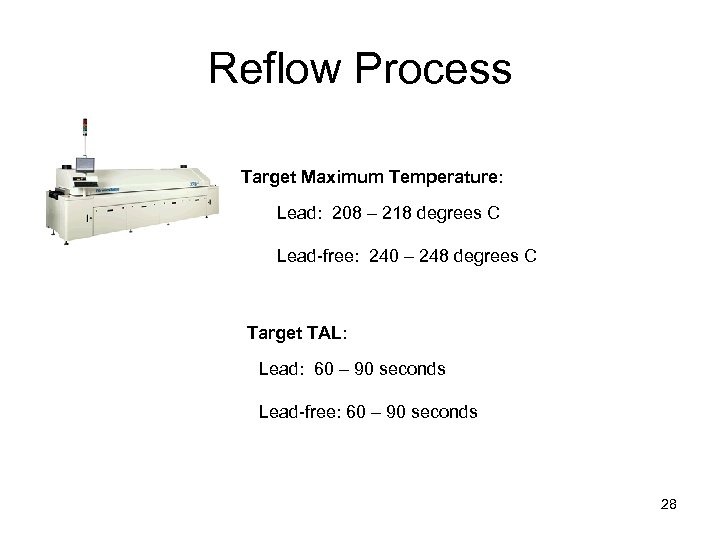 Reflow Process Target Maximum Temperature: Lead: 208 – 218 degrees C Lead-free: 240 – 248 degrees C Target TAL: Lead: 60 – 90 seconds Lead-free: 60 – 90 seconds 28
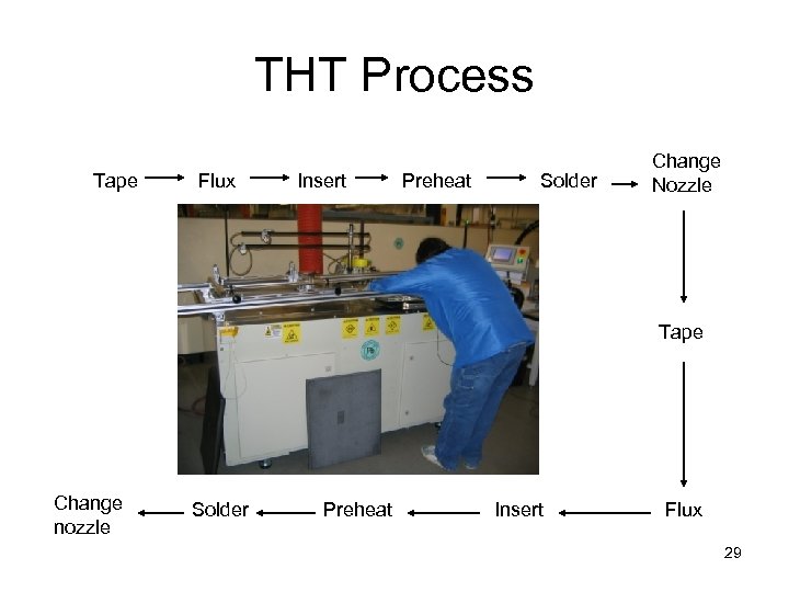 THT Process Tape Flux Insert Preheat Solder Change Nozzle Tape Change nozzle Solder Preheat Insert Flux 29
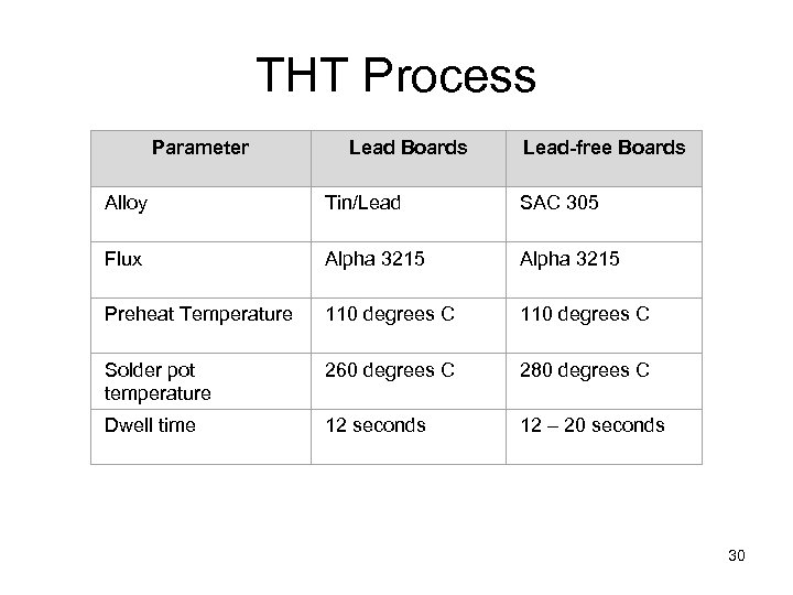 THT Process Parameter Lead Boards Lead-free Boards Alloy Tin/Lead SAC 305 Flux Alpha 3215 Preheat Temperature 110 degrees C Solder pot temperature 260 degrees C 280 degrees C Dwell time 12 seconds 12 – 20 seconds 30
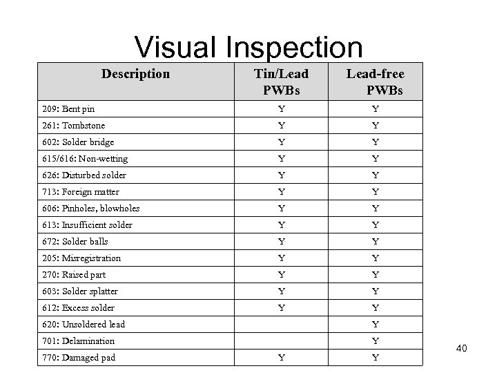
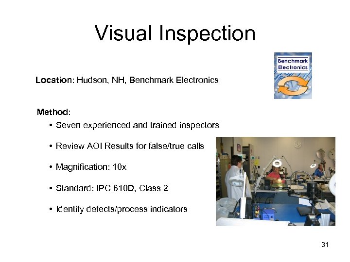 Visual Inspection Location: Hudson, NH, Benchmark Electronics Method: • Seven experienced and trained inspectors • Review AOI Results for false/true calls • Magnification: 10 x • Standard: IPC 610 D, Class 2 • Identify defects/process indicators 31
 Thermal Cycling Location: Andover, MA, Raytheon Method: Meet the requirements of IPC-9701, test condition TC 1 2, 000 Cycles Cycle Time: Approx. 40 minutes per cycle - Ramp rate: 10 degrees C per minute - 10 minute dwell time at 0 C - 10 minute dwell time at 100 C Equipment: Thermotron F 125 CHV 37 -30 32
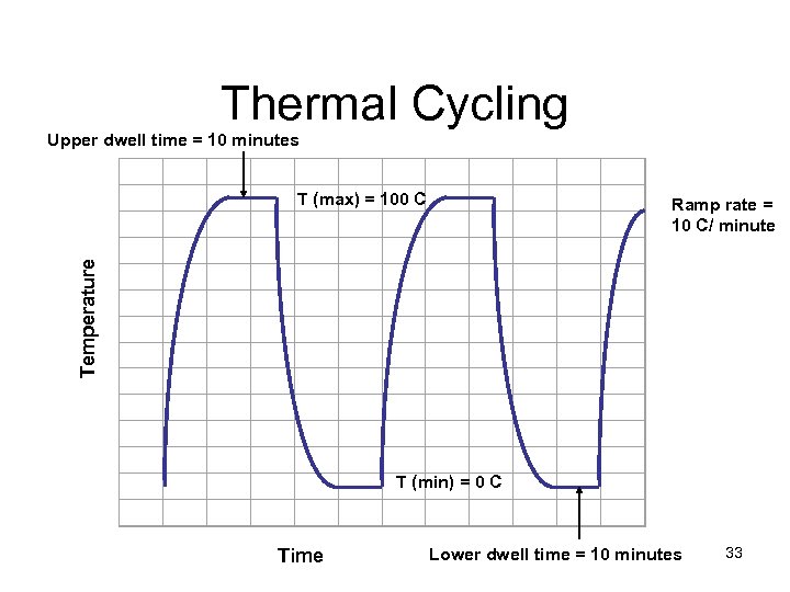 Thermal Cycling Upper dwell time = 10 minutes Temperature T T (max) = 100 C Time (min) = 0 C Ramp rate = 10 C/ minute Lower dwell time = 10 minutes 33
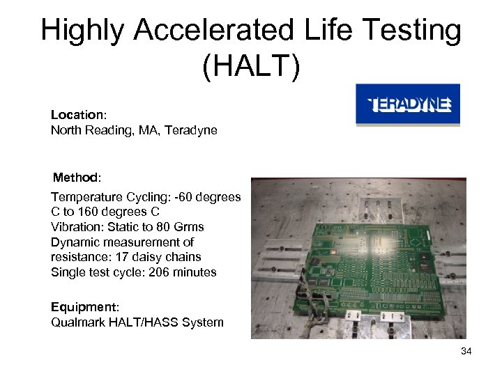 Highly Accelerated Life Testing (HALT) Location: North Reading, MA, Teradyne Method: Temperature Cycling: -60 degrees C to 160 degrees C Vibration: Static to 80 Grms Dynamic measurement of resistance: 17 daisy chains Single test cycle: 206 minutes Equipment: Qualmark HALT/HASS System 34
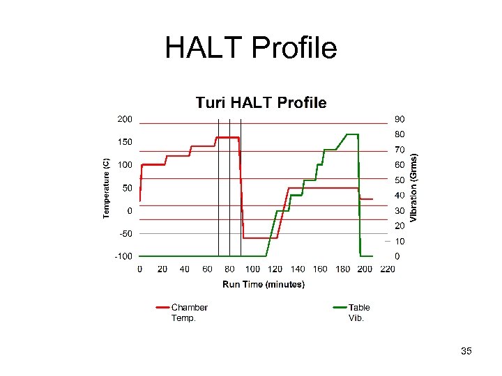 HALT Profile 35
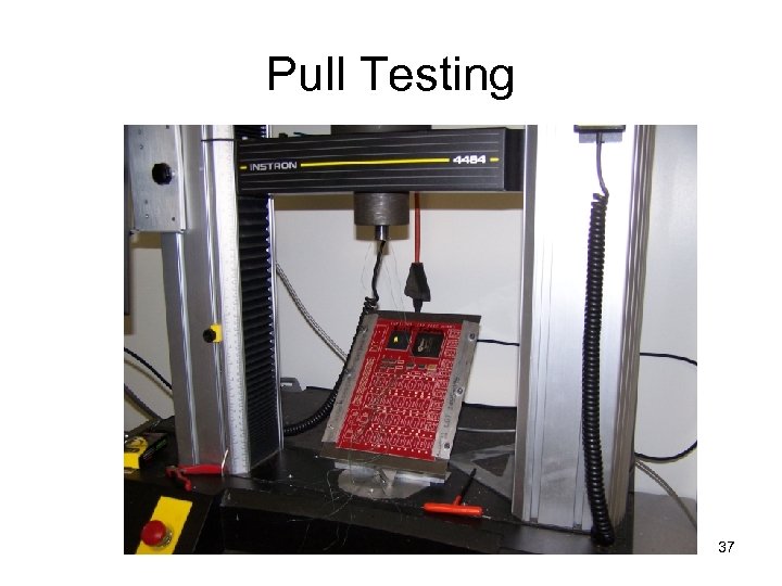
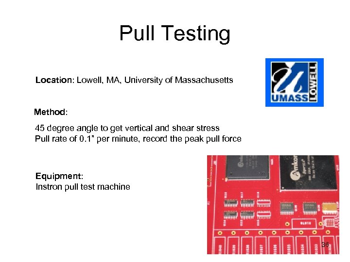 Pull Testing Location: Lowell, MA, University of Massachusetts Method: 45 degree angle to get vertical and shear stress Pull rate of 0. 1” per minute, record the peak pull force Equipment: Instron pull test machine 36
 Pull Testing 37
 Results & Conclusions 38
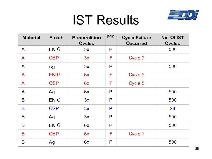 IST Results P/F Cycle Failure Occurred ENIG Precondition Cycles 3 x P No. Of IST Cycles 500 OSP 3 x F Cycle 3 Ag 3 x P 500 A ENIG 6 x F Cycle 5 A OSP 6 x F Cycle 5 A Ag 6 x P 500 B ENIG 3 x P 500 B OSP 3 x P 29 B Ag 3 x P 500 B ENIG 6 x P 500 B OSP 6 x F Cycle 1 B Ag 6 x P 500 Material Finish A A A 39
 Visual Inspection Description Tin/Lead PWBs Lead-free PWBs 209: Bent pin Y Y 261: Tombstone Y Y 602: Solder bridge Y Y 615/616: Non-wetting Y Y 626: Disturbed solder Y Y 713: Foreign matter Y Y 606: Pinholes, blowholes Y Y 613: Insufficient solder Y Y 672: Solder balls Y Y 205: Misregistration Y Y 270: Raised part Y Y 603: Solder splatter Y Y 612: Excess solder Y Y 620: Unsoldered lead Y 701: Delamination Y 770: Damaged pad Y Y 40
 Total Components Per Board Lead-free (24 Boards) Tin/Lead (12 Boards) Totals SMT 1, 713 41, 112 20, 556 61, 668 THT 53 636 318 954 1, 766 41, 748 20, 874 62, 622 Total Defects Lead-free 24 Boards (x 2 inspections) Tin/Lead 12 Boards (x 2 inspections) Totals SMT 377 349 726 THT 246 21 267 Totals 623 370 993 41
 Defects Per Unit (Board) Lead-free (24 Boards) Tin/Lead (12 Boards) Totals SMT 7. 8 14. 5 10. 1 THT 10. 2 1. 7 7. 4 Defects Per Unit (Component) Lead-free (24 Boards) Tin/Lead (12 Boards) Totals SMT 0. 005 0. 008 0. 006 THT 0. 193 0. 033 0. 144 42
 Visual Inspection Summary DOE 1 - Lead-free Boards: • For THT components, there is no statistical difference for solder paste supplier, surface finish, or laminate material supplier. • For SMT components, there is borderline statistical difference for solder paste supplier and laminate supplier. There is no statistical difference for surface finish. • There is a statistical difference for the interaction of solder paste supplier and laminate material supplier for SMT components. Best SMT Combination: Laminate “Z”, ENIG, either paste 43
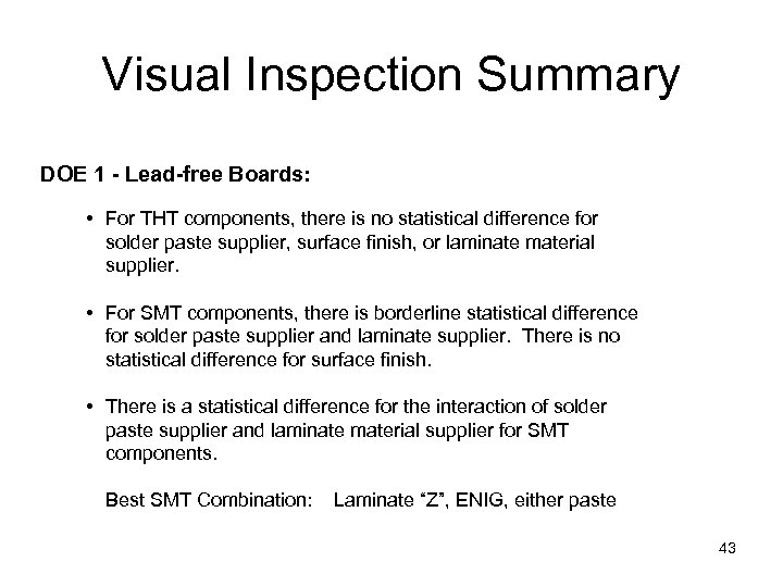
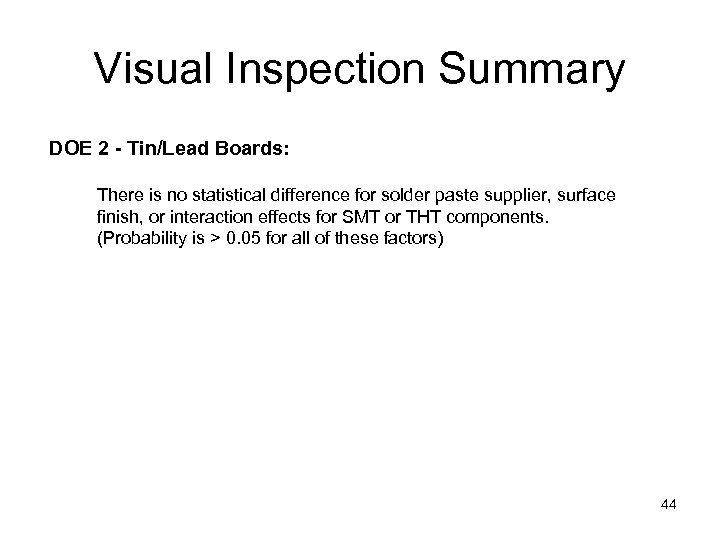 Visual Inspection Summary DOE 2 - Tin/Lead Boards: There is no statistical difference for solder paste supplier, surface finish, or interaction effects for SMT or THT components. (Probability is > 0. 05 for all of these factors) 44
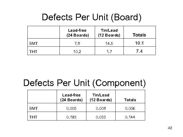
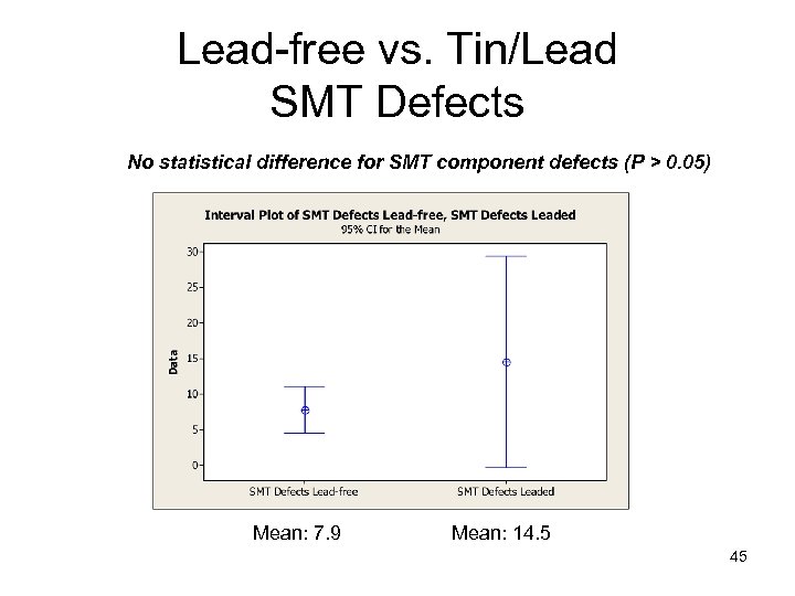 Lead-free vs. Tin/Lead SMT Defects No statistical difference for SMT component defects (P > 0. 05) Mean: 7. 9 Mean: 14. 5 45
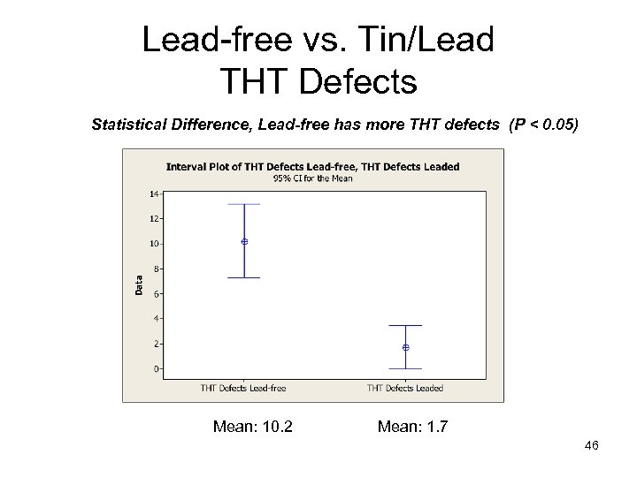 Lead-free vs. Tin/Lead THT Defects Statistical Difference, Lead-free has more THT defects (P < 0. 05) Mean: 10. 2 Mean: 1. 7 46
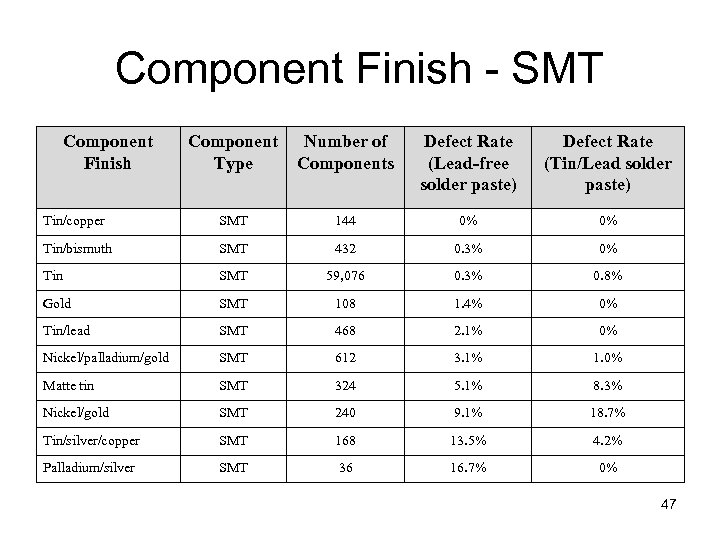 Component Finish - SMT Component Finish Component Type Number of Components Defect Rate (Lead-free solder paste) Defect Rate (Tin/Lead solder paste) Tin/copper SMT 144 0% 0% Tin/bismuth SMT 432 0. 3% 0% Tin SMT 59, 076 0. 3% 0. 8% Gold SMT 108 1. 4% 0% Tin/lead SMT 468 2. 1% 0% Nickel/palladium/gold SMT 612 3. 1% 1. 0% Matte tin SMT 324 5. 1% 8. 3% Nickel/gold SMT 240 9. 1% 18. 7% Tin/silver/copper SMT 168 13. 5% 4. 2% Palladium/silver SMT 36 16. 7% 0% 47
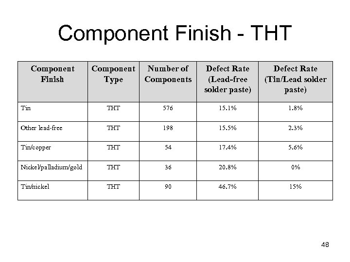 Component Finish - THT Component Finish Component Type Number of Components Defect Rate (Lead-free solder paste) Defect Rate (Tin/Lead solder paste) Tin THT 576 15. 1% 1. 8% Other lead-free THT 198 15. 5% 2. 3% Tin/copper THT 54 17. 4% 5. 6% Nickel/palladium/gold THT 36 20. 8% 0% Tin/nickel THT 90 46. 7% 15% 48
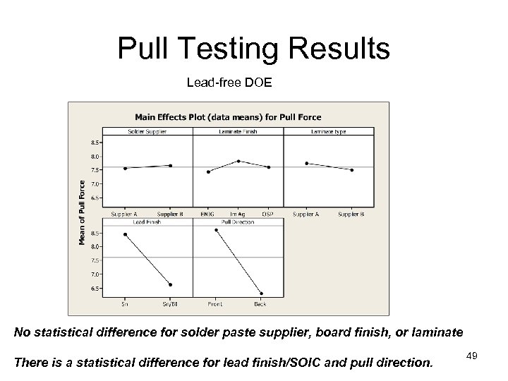 Pull Testing Results Lead-free DOE No statistical difference for solder paste supplier, board finish, or laminate There is a statistical difference for lead finish/SOIC and pull direction. 49
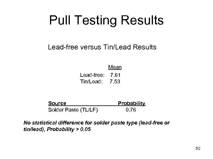 Pull Testing Results Lead-free versus Tin/Lead Results Mean Lead-free: 7. 61 Tin/Lead: 7. 53 Source Probability Solder Paste (TL/LF) 0. 76 No statistical difference for solder paste type (lead-free or tin/lead), Probability > 0. 05 50
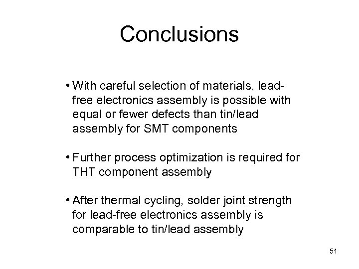 Conclusions • With careful selection of materials, leadfree electronics assembly is possible with equal or fewer defects than tin/lead assembly for SMT components • Further process optimization is required for THT component assembly • After thermal cycling, solder joint strength for lead-free electronics assembly is comparable to tin/lead assembly 51
 Next Steps Further inspection and X-ray of HALT boards Electrical testing of certain components Further testing and optimization for THT components Vitronics selective solder machine, Phase III boards & components, Dwell time, solder pot temperature, flux, etc. Develop a Failure Modes and Effect Analysis (FMEA) Potential failure modes, severity of effect, probability of occurrence, detection capability, and recommended mitigation actions 52
 Multiwave Technology 53
 Select Wave Technology 54
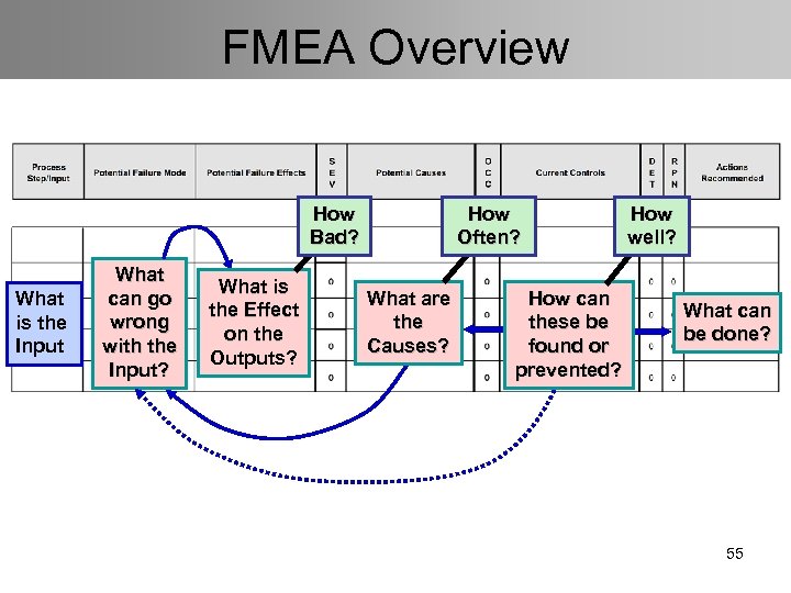 FMEA Overview How Bad? What is the Input What can go wrong with the Input? What is the Effect on the Outputs? How Often? What are the Causes? How can these be found or prevented? How well? What can be done? 55
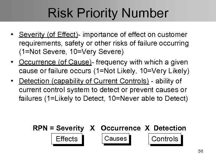 Risk Priority Number • Severity (of Effect)- importance of effect on customer requirements, safety or other risks of failure occurring (1=Not Severe, 10=Very Severe) • Occurrence (of Cause)- frequency with which a given cause or failure occurs (1=Not Likely, 10=Very Likely) • Detection (capability of Current Controls) - ability of current control system to detect or prevent causes or failures (1=Likely to Detect, 10=Never able to Detect) RPN = Severity X Occurrence X Detection Effects Causes Controls 56
 Consortium Information For further information about the consortium, please contact: Greg Morose Toxics Use Reduction Institute (978) 934 -2954 Gregory_Morose@uml. edu Or visit our website: http: //www. turi. org/content/view/full/339/ 57


