ee0f46e71774ac005f0dfb0801d3bb9e.ppt
- Количество слайдов: 30
New Burn In (BI) Methodology for testing of blank Actel 0. 15 m RTAX-S FPGAs September 7 th – 9 th, 2005 Minal Sawant Solomon Wolday Paul Louris Dan Elftmann
Introduction <This paper will cover a new approach adopted by Actel to implement the burn in testing of RTAX-S devices using the INCAL state of the art burn in test system <INCAL provided all of the elements needed for a complete operational system including: = Test vector pattern generator which accepts the IEEE 1149. 11 SVF (Serial Vector Format) and pattern editor configured to Actel’s requirements for 80 MB <Actel worked with INCAL to develop a modified driver board for deep JTAG test stimulus to enable node toggle coverage of the advanced RTAX-S feature set to implement the Dynamic Blank Burn-In (DBBI) Sawant, Wolday, Louris, Elftmann 2 New BI Methodology MAPLD 2005 / #239
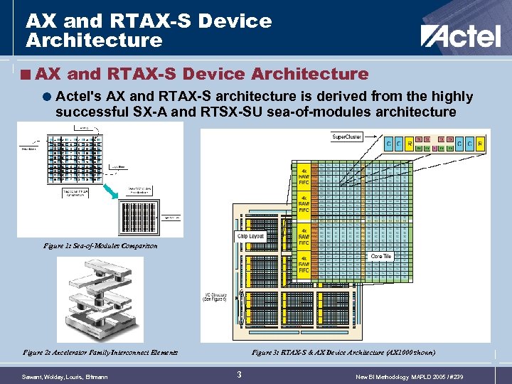
AX and RTAX-S Device Architecture <AX and RTAX-S Device Architecture = Actel's AX and RTAX-S architecture is derived from the highly successful SX-A and RTSX-SU sea-of-modules architecture Figure 1: Sea-of-Modules Comparison Figure 2: Axcelerator Family Interconnect Elements Sawant, Wolday, Louris, Elftmann Figure 3: RTAX-S & AX Device Architecture (AX 1000 shown) 3 New BI Methodology MAPLD 2005 / #239
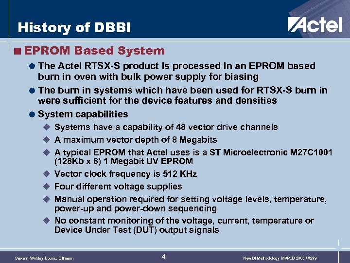
History of DBBI <EPROM Based System = The Actel RTSX-S product is processed in an EPROM based burn in oven with bulk power supply for biasing = The burn in systems which have been used for RTSX-S burn in were sufficient for the device features and densities = System capabilities u Systems have a capability of 48 vector drive channels u A maximum vector depth of 8 Megabits u A typical EPROM that Actel uses is a ST Microelectronic M 27 C 1001 (128 Kb x 8) 1 Megabit UV EPROM u Vector clock frequency is 512 KHz u Four different voltage supplies u Manual operation required for setting voltage levels, temperature, power-up and power-down sequencing u No constant monitoring of the voltage, current, temperature or Device Under Test (DUT) output signals Sawant, Wolday, Louris, Elftmann 4 New BI Methodology MAPLD 2005 / #239
History of DBBI < Limitation of EPROM for RTAX-S and the switch to INCAL = Several limitations exist in the EPROM based burn in system u u No system control No system voltage and current monitoring capabilities No DUT monitoring capabilities Limited vector depth of 8 Megabits = Distinct advantages of INCAL Tracer I 160 Burn in system over traditional burn in methodologies u Automated upload sequence of lot u Constant monitoring of the system, DUT input and DUT output signals during burn in u Deep vector capability (>200 Megabit) u Existing INCAL Tracer I 160 Burn in system had a limitation in vector depth u Actel worked closely with INCAL to add the deep vector capability to the INCAL Tracer I 160 driver board u Software support added to translate Teradyne J 750 ATP test vector format to Serial Vector Format (SVF) format u Software support added for SVF The Serial Vector Format was developed as a vendor-independent method to represent JTAG (IEEE 1149. 1) test patterns in ASCII (text) files Sawant, Wolday, Louris, Elftmann 5 New BI Methodology MAPLD 2005 / #239
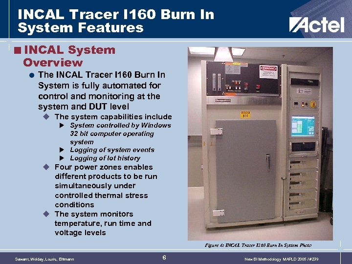
INCAL Tracer I 160 Burn In System Features <INCAL System Overview = The INCAL Tracer I 160 Burn In System is fully automated for control and monitoring at the system and DUT level u The system capabilities include u System controlled by Windows 32 bit computer operating system u Logging of system events u Logging of lot history u Four power zones enables different products to be run simultaneously under controlled thermal stress conditions u The system monitors temperature, run time and voltage levels Figure 4: INCAL Tracer I 160 Burn In System Photo Sawant, Wolday, Louris, Elftmann 6 New BI Methodology MAPLD 2005 / #239
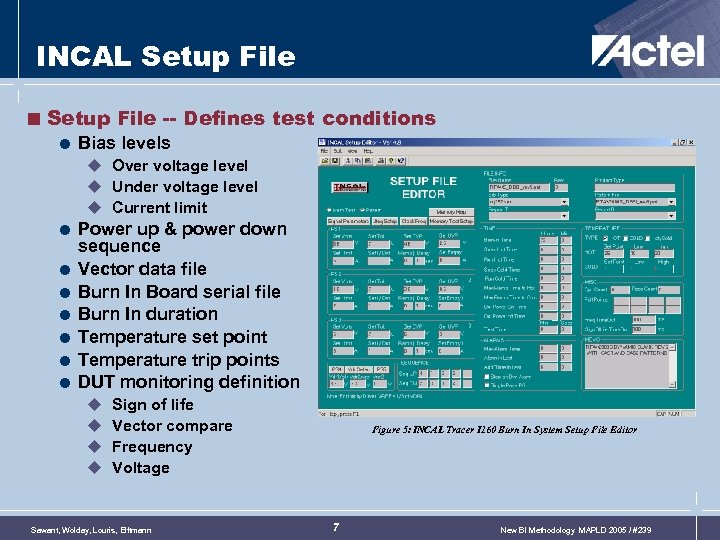
INCAL Setup File < Setup File -- Defines test conditions = Bias levels u Over voltage level u Under voltage level u Current limit = Power up & power down sequence = Vector data file = Burn In Board serial file = Burn In duration = Temperature set point = Temperature trip points = DUT monitoring definition u u Sign of life Vector compare Frequency Voltage Sawant, Wolday, Louris, Elftmann Figure 5: INCAL Tracer I 160 Burn In System Setup File Editor 7 New BI Methodology MAPLD 2005 / #239
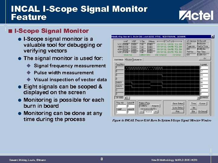
INCAL I-Scope Signal Monitor Feature < I-Scope Signal Monitor = I-Scope signal monitor is a valuable tool for debugging or verifying vectors = The signal monitor is used for: u Signal frequency measurement u Pulse width measurement u Visual inspection of vector data = Eight signals can be scoped & displayed on the screen = Monitoring is possible for each burn in board = Monitoring can be done at any time during the process Sawant, Wolday, Louris, Elftmann 8 Figure 6: INCAL Tracer I 160 Burn In System I-Scope Signal Monitor Window New BI Methodology MAPLD 2005 / #239
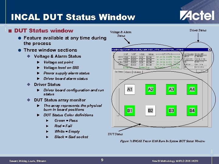
INCAL DUT Status Window < DUT Status window = Feature available at any time during the process = Three window sections Voltage & Alarm Status Driver Status u Voltage & Alarm Status u u Voltage set point Voltage level on BIB Power supply alarm status Driver board alarm status u Driver Status u Driver board configuration and run status u DUT Status array monitor u u The array represents the physical burn in board positions DUT Status Color definitions Green = Pass Red = Fail White = Empty Black = Bad socket DUT Status Figure 7: INCAL Tracer I 160 Burn In System DUT Status Window Sawant, Wolday, Louris, Elftmann 9 New BI Methodology MAPLD 2005 / #239
Burn In Of Actel FPGA’s <Burn In of Actel FPGAs = During blank device electrical testing, Actel devices are subjected to controlled voltage stress to the maximum operating conditions u Voltage stress testing of semiconductor devices is a much more effective screen than a temperature burn in = Actel takes advantage of the testability features of its FPGA products to provide effective dynamic burn in of blank devices = Burn in is required for all Mil. Std-883 “B” and “E” flow products u MIL-883 E Method 1005, allows several types of burn in screens, which can be divided into two categories: u Dynamic Blank Burn In (DBBI) u Static Blank Burn In (SBBI) Sawant, Wolday, Louris, Elftmann 10 New BI Methodology MAPLD 2005 / #239
Goal Of Burn In <DBBI = Dynamic burn in applies AC signals to device inputs = These signals are selected so that the device receives internal and external stresses similar to those it would experience in a typical application = A properly designed dynamic burn in can effectively stress inputs, outputs, and internal circuits = Actel performs DBBI for four main reasons: u u Stress un-programmed antifuses Stress internal CMOS logic Stress internal SRAM blocks Stress I/Os <SBBI = Static burn in applies DC voltage levels to the pins of the device under test with the device powered up = Static burn in can be an effective screen for mobile ionic contamination failure modes, which affect device inputs or outputs u Effective design of seal ring barriers and device passivation makes this type of contamination highly unlikely Sawant, Wolday, Louris, Elftmann 11 New BI Methodology MAPLD 2005 / #239
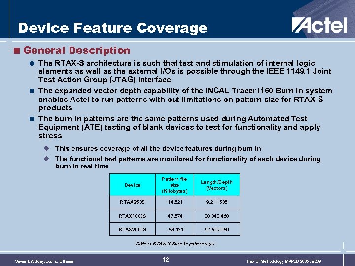
Device Feature Coverage < General Description = The RTAX-S architecture is such that test and stimulation of internal logic elements as well as the external I/Os is possible through the IEEE 1149. 1 Joint Test Action Group (JTAG) interface = The expanded vector depth capability of the INCAL Tracer I 160 Burn In system enables Actel to run patterns with out limitations on pattern size for RTAX-S products = The burn in patterns are the same patterns used during Automated Test Equipment (ATE) testing of blank devices to test for functionality and apply stress u This ensures coverage of all the device features during burn in u The functional test patterns are monitored for functionality of each device during burn in real time Device Pattern file size (Kilobytes) Length/Depth (Vectors) RTAX 250 S 14, 621 9, 211, 536 RTAX 1000 S 47, 674 30, 040, 480 RTAX 2000 S 83, 331 52, 509, 680 Table 1: RTAX-S Burn In pattern sizes Sawant, Wolday, Louris, Elftmann 12 New BI Methodology MAPLD 2005 / #239
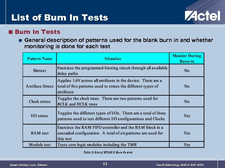
List of Burn In Tests < Burn In Tests = General description of patterns used for the blank burn in and whether monitoring is done for each test Table 2: List of RTAX-S Burn In tests Sawant, Wolday, Louris, Elftmann 13 New BI Methodology MAPLD 2005 / #239
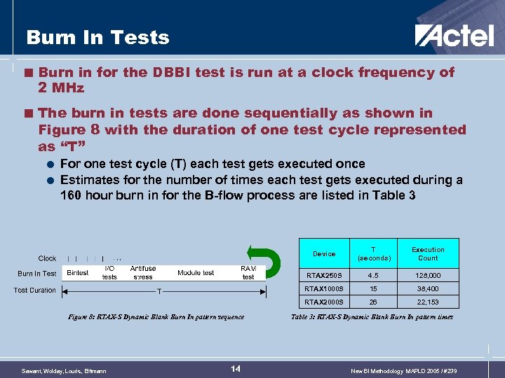
Burn In Tests < Burn in for the DBBI test is run at a clock frequency of 2 MHz < The burn in tests are done sequentially as shown in Figure 8 with the duration of one test cycle represented as “T” = For one test cycle (T) each test gets executed once = Estimates for the number of times each test gets executed during a 160 hour burn in for the B-flow process are listed in Table 3 Device 128, 000 15 38, 400 RTAX 2000 S 14 4. 5 RTAX 1000 S Sawant, Wolday, Louris, Elftmann Execution Count RTAX 250 S Figure 8: RTAX-S Dynamic Blank Burn In pattern sequence T (seconds) 26 22, 153 Table 3: RTAX-S Dynamic Blank Burn In pattern times New BI Methodology MAPLD 2005 / #239
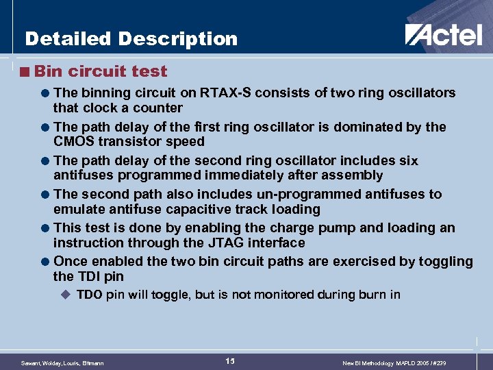
Detailed Description <Bin circuit test = The binning circuit on RTAX-S consists of two ring oscillators that clock a counter = The path delay of the first ring oscillator is dominated by the CMOS transistor speed = The path delay of the second ring oscillator includes six antifuses programmed immediately after assembly = The second path also includes un-programmed antifuses to emulate antifuse capacitive track loading = This test is done by enabling the charge pump and loading an instruction through the JTAG interface = Once enabled the two bin circuit paths are exercised by toggling the TDI pin u TDO pin will toggle, but is not monitored during burn in Sawant, Wolday, Louris, Elftmann 15 New BI Methodology MAPLD 2005 / #239
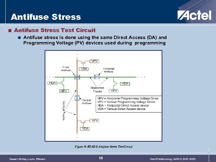
Antifuse Stress < Antifuse Stress Test Circuit = Antifuse stress is done using the same Direct Access (DA) and Programming Voltage (PV) devices used during programming Figure 9: RTAX-S Antifuse Stress Test Circuit Sawant, Wolday, Louris, Elftmann 16 New BI Methodology MAPLD 2005 / #239
Antifuse Stress < Cross Antifuse = Cross Antifuse Stress patterns switch the voltage across the cross antifuses in the FPGA = This is done using the same DA and PV devices used during programming = During this test, all cross antifuses, clock antifuses and input class antifuses are stressed < I/O Antifuse Stress = I/O configuration antifuses are stressed in alternate directions = This is done via separate patterns in a manner similar to the cross antifuse stress patterns = During this test the I/O bank configuration antifuses are also stressed < Horizontal and Vertical Antifuses = These two patterns apply a stress pattern to the horizontal and vertical antifuses in alternate directions = These antifuses are utilized to extend horizontal and vertical segments = This is done using a similar methodology as the cross antifuse stress patterns with specific adjustments for the horizontal and vertical antifuse addressing scheme Sawant, Wolday, Louris, Elftmann 17 New BI Methodology MAPLD 2005 / #239
I/O Test < Clock Tests = Two patterns are used for this test to stimulate both the routed and the hardwired clock trees = The output stage of the clock multiplexers is toggled during these patterns < I/O test = Three patterns are used to toggle the different I/O standards = The aim of single ended I/O stress is to toggle all single-ended I/O input and output buffers in the device u This is done using the JTAG Boundary Scan Register (BSR) = All I/O pads including un-bonded I/O pads get exercised = The I/O pads are driven through states “high”, “tristate” and “low” levels during burn in u These states are driven on output buffers and read back at the input buffers as shown in Figure 10 on next slide Sawant, Wolday, Louris, Elftmann 18 New BI Methodology MAPLD 2005 / #239
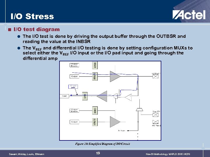
I/O Stress < I/O test diagram = The I/O test is done by driving the output buffer through the OUTBSR and reading the value at the INBSR = The VREF and differential I/O testing is done by setting configuration MUXs to select either the VREF I/O input or the I/O pad input and going through the differential amp Figure 10: Simplified Diagram of I/O Circuit Sawant, Wolday, Louris, Elftmann 19 New BI Methodology MAPLD 2005 / #239
Core Logic Module Tests < Core logic modules are exercised and monitored during burn in with the Core Logic Module Tests = Combinatorial logic = Sequential logic = Buffer u The Buffer module takes a regular routed signal from the horizontal channel in the same row or the row to the North and drives its own Output-track = TX and RX u The TX module provides transmission capability to the horizontal and vertical highway channels u The RX module receives a signal from a horizontal highway channel in the same row or a vertical highway channel in the same Super. Cluster column and transfers it to its own Output track for distribution with regular routing means = Carry chain u Logic modules in a column are linked into a carry-chain running from North to South u They provide high-speed propagation of carry logic for ripple style arithmetic functions u Carry-connect module utilizes a hardwired signal path which does not require a programmable interconnection Sawant, Wolday, Louris, Elftmann 20 New BI Methodology MAPLD 2005 / #239
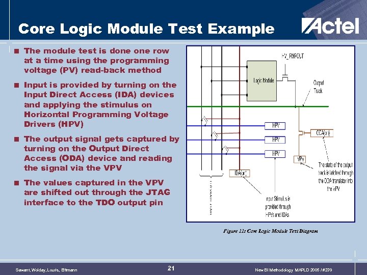
Core Logic Module Test Example < The module test is done row at a time using the programming voltage (PV) read-back method < Input is provided by turning on the Input Direct Access (IDA) devices and applying the stimulus on Horizontal Programming Voltage Drivers (HPV) < The output signal gets captured by turning on the Output Direct Access (ODA) device and reading the signal via the VPV < The values captured in the VPV are shifted out through the JTAG interface to the TDO output pin Figure 11: Core Logic Module Test Diagram Sawant, Wolday, Louris, Elftmann 21 New BI Methodology MAPLD 2005 / #239
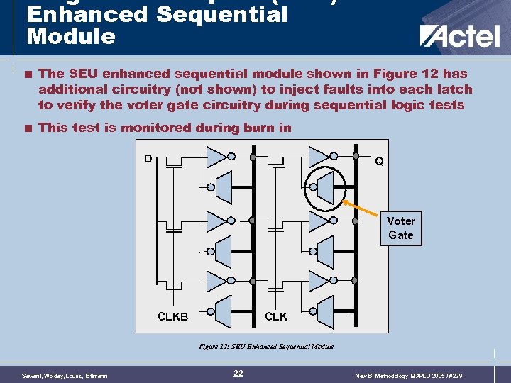
Single Event Upset (SEU) Enhanced Sequential Module < The SEU enhanced sequential module shown in Figure 12 has additional circuitry (not shown) to inject faults into each latch to verify the voter gate circuitry during sequential logic tests < This test is monitored during burn in D Q Voter Gate CLKB CLK Figure 12: SEU Enhanced Sequential Module Sawant, Wolday, Louris, Elftmann 22 New BI Methodology MAPLD 2005 / #239
SRAM/FIFO Test < SRAM/FIFO test = There are four Built In Self Test (BIST) tests designed to test the FIFO counters for SRAM cascaded configurations = All blocks on the chip are simultaneously tested = FIFO logic for each block is cycled through the complete addressing sequences for all possible configuration depths = Test Methodology u There are three sections of Cyclic Redundancy Code (CRC) registers in each SRAM/FIFO block u Each section collects the test response from a specific type of circuit u Shifting control data into the SRAM/FIFO blocks through the tap port operates the BIST u The CRC signature result from running the BIST test is shifted out and compared against expected value from simulation Sawant, Wolday, Louris, Elftmann 23 New BI Methodology MAPLD 2005 / #239
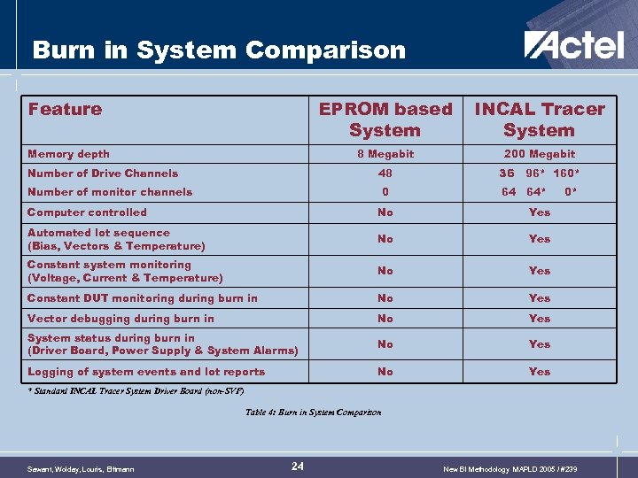
Burn in System Comparison Feature EPROM based System 8 Megabit Memory depth INCAL Tracer System 200 Megabit 48 36 96* 160* 0 Number of Drive Channels 64 64* Number of monitor channels Computer controlled No Yes Automated lot sequence (Bias, Vectors & Temperature) No Yes Constant system monitoring (Voltage, Current & Temperature) No Yes Constant DUT monitoring during burn in No Yes Vector debugging during burn in No Yes System status during burn in (Driver Board, Power Supply & System Alarms) No Yes Logging of system events and lot reports No 0* Yes * Standard INCAL Tracer System Driver Board (non-SVF) Table 4: Burn in System Comparison Sawant, Wolday, Louris, Elftmann 24 New BI Methodology MAPLD 2005 / #239
Conclusion < Thru partnership with INCAL Technology, Inc. Actel was able to leverage industry standards (IEEE 1149. 1) to develop a system that can be used for devices and technologies beyond Actel FPGAs < Actel has successfully implemented a new burn in methodology for the Axcelerator architecture = Significantly increased visibility into burn in operations u Complete system control u Constant monitoring of DUT functionality u Constant monitoring of voltage, temperature and current = System enables quicker turn around time for continuous enhancements of test coverage u ATE test patterns are easily converted to SVF format u Expanded vector depth capability enables Actel to run patterns with fewer limitations on pattern size u Ability of real time debug during burn in u Logging of system events and lot status Sawant, Wolday, Louris, Elftmann 25 New BI Methodology MAPLD 2005 / #239

Appendix Axcelerator Architecture
Embedded Memory < Each core tile has either three (AX 250 & RTAX 250 S) or four (All other devices) embedded SRAM blocks along the west side < Each variable-aspect-ratio SRAM block is 4 Kbits in size < Available memory configurations are: = 128 x 36, 256 x 18, 512 x 9, 1 K x 4, 2 K x 2 or 4 K x 1 bits < The individual blocks have separate read and write ports that can be configured with different bit widths on each port = For example, data can be written in by 8 and read out by 1 < The embedded SRAM/FIFO blocks can be cascaded to create larger configurations < The embedded SRAM blocks can be initialized at power up via the device JTAG port (ROM emulation mode) Sawant, Wolday, Louris, Elftmann 27 New BI Methodology MAPLD 2005 / #239
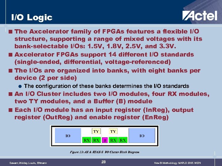
I/O Logic < The Axcelerator family of FPGAs features a flexible I/O structure, supporting a range of mixed voltages with its bank-selectable I/Os: 1. 5 V, 1. 8 V, 2. 5 V, and 3. 3 V. < Axcelerator FPGAs support 14 different I/O standards (single-ended, differential, voltage-referenced) < The I/Os are organized into banks, with eight banks per device (2 per side) = The configuration of these banks determines the I/O standards < An I/O Cluster includes two I/O modules, four RX modules, two TY modules, and a Buffer (B) module < Each I/O module has an input register (In. Reg), output register (Out. Reg) and enable register (En. Reg) Figure 13: AX & RTAX-S I/O Cluster Block Diagram Sawant, Wolday, Louris, Elftmann 28 New BI Methodology MAPLD 2005 / #239
Routing and Resources < The AX & RTAX-S hierarchical routing structure ties the logic modules, the embedded memory blocks, and the I/O modules together = The level 1 routing structures -- Figure 14 on next slide u In and between Super. Clusters are three local routing structures: u Fast. Connects provide high-performance horizontal routing inside the Super. Cluster and vertical routing to the Super. Cluster immediately below it Only one programmable connection is used in a Fast. Connect path u Carry. Connect routing Carry. Connects are used for routing carry logic between adjacent Super. Clusters They connect the Fast. Connect output (FCO) of one 2 -bit, C-cell carry logic to the Fast. Connect Input (FCI) of the 2 -bit, C-cell carry logic of the Super. Cluster below it Carry. Connects do not require an antifuse to make the connection u Direct. Connects provide the highest performance routing inside the Super. Clusters connecting the C-cell to the adjacent R-cell Direct. Connects do not require an antifuse to make the connection Sawant, Wolday, Louris, Elftmann 29 New BI Methodology MAPLD 2005 / #239
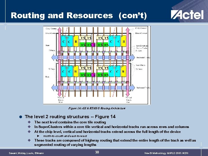
Routing and Resources (con’t) Figure 14: AX & RTAX-S Routing Architecture = The level 2 routing structures -- Figure 14 u u u The next level contains the core tile routing In Super. Clusters within a core tile vertical and horizontal tracks run across rows and columns At the chip level, vertical and horizontal tracks extend across the full length of the device u u north-to-south and east-to-west These tracks are composed of highway routing that extend the entire length of the track as well as segmented routing of varying lengths Sawant, Wolday, Louris, Elftmann 30 New BI Methodology MAPLD 2005 / #239
ee0f46e71774ac005f0dfb0801d3bb9e.ppt