Членова.ppt
- Количество слайдов: 8
 Nanostructured Magnetoimpedance Multilayers G. V. Kurlyandskaya 1, 2, A. García-Arribas 1, E. Fernández 1, and A. V. Svalov 1, 3 1 Departamento de Electricidad y Electrónica, Universidad del País Vasco, Bilbao, Spain 2 Department of Physics, University of Maryland, College Park, MD USA 3 Department of Magnetism and Magnetic Nanomaterials, Ural Federal University, Ekaterinburg, Russia About publication: IEEE Transactions on Magnetics, Vol. 48, No. 4, April 2012 DOI: 10. 1109/TMAG. 2011. 2171330 Reporter Anna Chlenova, group ЕНМ-140125
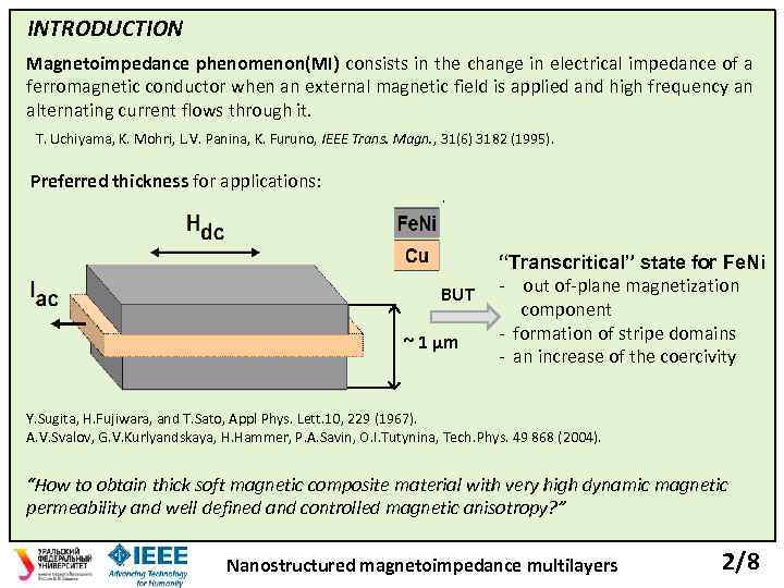 INTRODUCTION Magnetoimpedance phenomenon(MI) consists in the change in electrical impedance of a ferromagnetic conductor when an external magnetic field is applied and high frequency an alternating current flows through it. T. Uchiyama, K. Mohri, L. V. Panina, K. Furuno, IEEE Trans. Magn. , 31(6) 3182 (1995). Preferred thickness for applications: BUT ~ 1 μm “Transcritical” state for Fe. Ni - out of-plane magnetization component - formation of stripe domains - an increase of the coercivity Y. Sugita, H. Fujiwara, and T. Sato, Appl Phys. Lett. 10, 229 (1967). A. V. Svalov, G. V. Kurlyandskaya, H. Hammer, P. A. Savin, O. I. Tutynina, Tech. Phys. 49 868 (2004). “How to obtain thick soft magnetic composite material with very high dynamic magnetic permeability and well defined and controlled magnetic anisotropy? ” Nanostructured magnetoimpedance multilayers 2/8
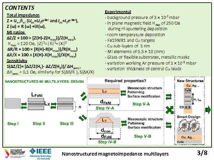 CONTENTS Total impedance Z = Uac/Iac (Uac=U 0 e-i t and Iac=I 0 e–i t), Z (ω) = R (ω) +i. X(ω), MI ratios ΔΖ/Ζ = 100 × [Z(H)-Z(Hmax)]/Z(Hmax), Hmax = 120 Oe, |Z|2=|R|2+|X|2 ΔR/R = 100 × [R(H)-R(H max)]/R(Hmax) ΔX/X = 100 × [X(H)-X(Hmax)]/X(Hmax) Sensitivity S(ΔΖ/Ζ)= [ΔΖ/Ζ(H 1)- ΔΖ/Ζ(H 2)]/ ΔHsens , ΔHsens = 0, 1 Oe, similarly for S(ΔR/R ), S(ΔX/X) Experimental - background pressure of 3 × 10 -7 mbar - in plane magnetic field Hdep of 250 Oe during rf-sputtering deposition - room temperature deposition - Fe 19 Ni 81 and Cu targets - Cu sub-layers of 3 nm - MI elements of 0. 5 × 10 (mm) - Glass or flexible substrates, metallic masks - variation working Ar pressure of 3 × 10 -3 mbar - variation thickness of central Cu leads Nanostructured magnetoimpedance multilayers 3/8
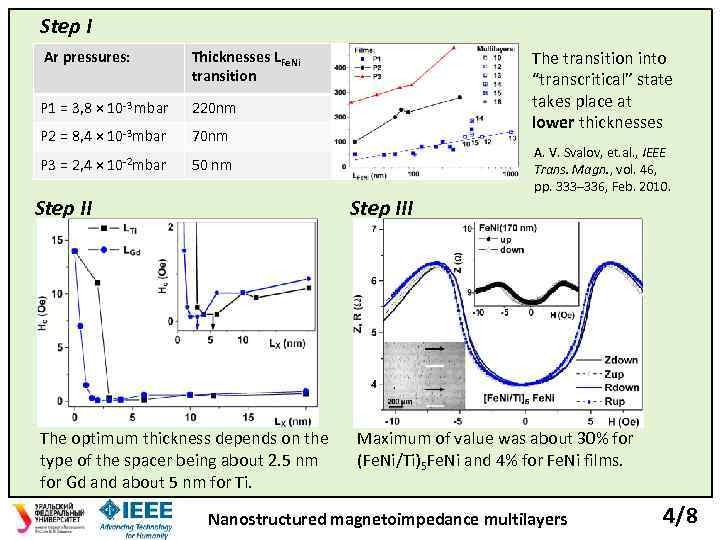 Step I Ar pressures: P 1 = 3, 8 × 10 -3 mbar 220 nm P 2 = 8, 4 × 10 -3 mbar 70 nm P 3 = 2, 4 × 10 -2 mbar The transition into “transcritical” state takes place at lower thicknesses Thicknesses LFe. Ni transition 50 nm Step III The optimum thickness depends on the type of the spacer being about 2. 5 nm for Gd and about 5 nm for Ti. A. V. Svalov, et. al. , IEEE Trans. Magn. , vol. 46, pp. 333– 336, Feb. 2010. Maximum of value was about 30% for (Fe. Ni/Ti)5 Fe. Ni and 4% for Fe. Ni films. Nanostructured magnetoimpedance multilayers 4/8
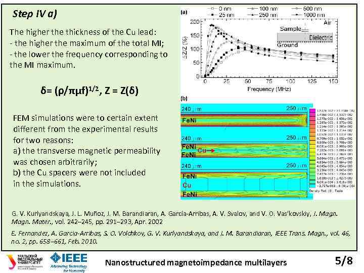 Step IV a) The higher the thickness of the Cu lead: - the higher the maximum of the total MI; - the lower the frequency corresponding to the MI maximum. δ= (ρ/πμf)1/2, Z = Z(δ) FEM simulations were to certain extent different from the experimental results for two reasons: a) the transverse magnetic permeability was chosen arbitrarily; b) the Cu spacers were not included in the simulations. G. V. Kurlyandskaya, J. L. Muñoz, J. M. Barandiaran, A. García-Arribas, A. V. Svalov, and V. O. Vas’kovskiy, J. Magn. Mater. , vol. 242– 245, pp. 291– 293, Apr. 2002 E. Fernandez, A. Garcia-Arribas, S. O. Volchkov, G. V. Kurlyandskaya, and J. M. Barandiaran, IEEE Trans. Magn. , vol. 46, no. 2, pp. 658– 661, Feb. 2010. Nanostructured magnetoimpedance multilayers 5/8
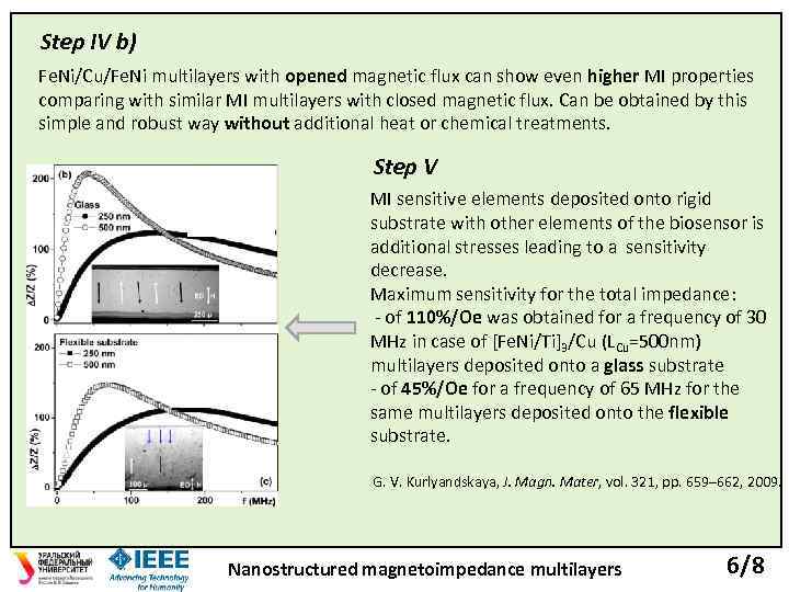 Step IV b) Fe. Ni/Cu/Fe. Ni multilayers with opened magnetic flux can show even higher MI properties comparing with similar MI multilayers with closed magnetic flux. Can be obtained by this simple and robust way without additional heat or chemical treatments. Step V MI sensitive elements deposited onto rigid substrate with other elements of the biosensor is additional stresses leading to a sensitivity decrease. Maximum sensitivity for the total impedance: - of 110%/Oe was obtained for a frequency of 30 MHz in case of [Fe. Ni/Ti]3/Cu (LCu=500 nm) multilayers deposited onto a glass substrate - of 45%/Oe for a frequency of 65 MHz for the same multilayers deposited onto the flexible substrate. G. V. Kurlyandskaya, J. Magn. Mater, vol. 321, pp. 659– 662, 2009. Nanostructured magnetoimpedance multilayers 6/8
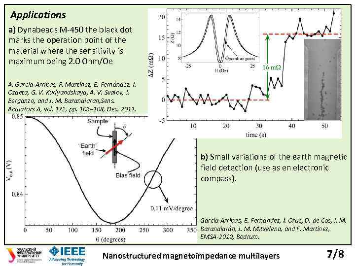 Applications a) Dynabeads M-450 the black dot marks the operation point of the material where the sensitivity is maximum being 2. 0 Ohm/Oe A. Garcia-Arribas, F. Martínez, E. Fernández, I. Ozaeta, G. V. Kurlyandskaya, A. V. Svalov, J. Berganzo, and J. M. Barandiaran, Sens. Actuators A, vol. 172, pp. 103– 108, Dec. 2011. b) Small variations of the earth magnetic field detection (use as en electronic compass). García-Arribas, E. Fernández, I. Orue, D. de Cos, J. M. Barandiarán, J. M. Mitxelena, and F. Martínez, EMSA-2010, Bodrum. Nanostructured magnetoimpedance multilayers 7/8
 SUMMARY AND OUTLOOK Thin Fe. Ni-based nanostructures were prepared by rf-sputtering. Comparative analysis of magnetic properties, domain structure and MI can be useful for the design of the magnetic nanostructures for high frequency applications. A maximum sensitivity of the total impedance of 110%/Oe at 30 MHz was obtained for multilayers deposited onto glass substrate (45%/Oe, at 65 MHz for the same multilayers deposited onto a flexible substrate). These values do indicate a capacity of optimized nanostructured Fe. Ni multilayers to be very competitive materials for magnetic field sensitive elements. Thank you for you attention! Nanostructured magnetoimpedance multilayers 8/8


