b87fe49bade25e42e817c4999228720b.ppt
- Количество слайдов: 24
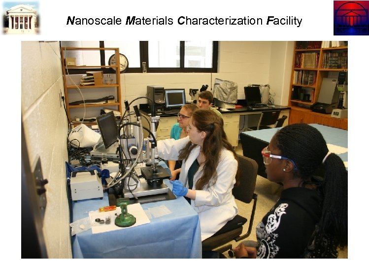 Nanoscale Materials Characterization Facility
 Nanoscale Materials Characterization Facility Operational Summary The Nanoscale Materials Characterization Facility (NMCF) is a state-of-the-art user facility located with the Materials Science and Engineering Dept (MSE). The facility is dedicated to materials characterization, available for use by all qualified faculty, students and researchers at UVa, as well as by researchers from other universities and industries. Scheduling is handled on a first-come first-serve basis by our web-based sign-up system. Technicians, students and faculty are available to assist researchers using the instruments, and courses in electron microscopy and materials characterization are offered each year. Capabilities Include: Atomic imaging of materials Elemental analysis Elemental mapping and energy-filtered imaging Dynamic experiments utilizing heating, cooling and straining holders Orientation mapping of materials Microstructural characterization Computer acquisition and processing of images and spectra
 Nanoscale Materials Characterization Facility NMCF Staff Michal Sabat: X-Ray Diffraction Specialist, Senior Staff Scientist University Of Virginia Depts. Chemistry and Materials Science & Engineering Phone: 434 -924 -7862 Email: ms 5 c@virginia. edu Richard R. White: Facility Manager, Staff Scientist University Of Virginia Department of Materials Science & Engineering Phone: 434 -982 -5657 Email: rrw 3 q@virginia. edu
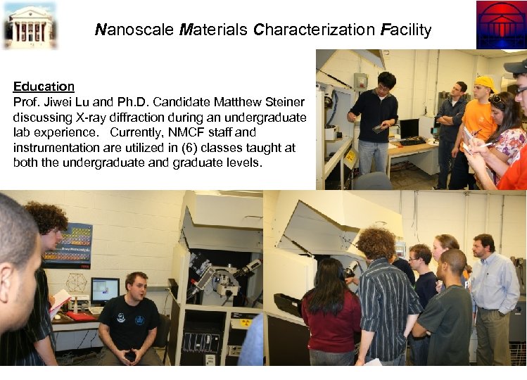 Nanoscale Materials Characterization Facility Education Prof. Jiwei Lu and Ph. D. Candidate Matthew Steiner discussing X-ray diffraction during an undergraduate lab experience. Currently, NMCF staff and instrumentation are utilized in (6) classes taught at both the undergraduate and graduate levels.
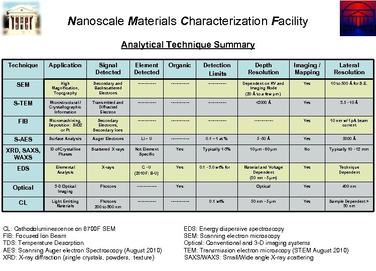 Nanoscale Materials Characterization Facility Analytical Technique Summary Technique Application Signal Detected Element Detected Organic Detection Limits Depth Resolution Imaging / Mapping Lateral Resolution SEM High Magnification, Topography Secondary and Backscattered Electrons -------------- Dependent on KV and Imaging Mode (20 Ǻ to a few μm ) Yes 10 to 500 Ǻ for S. E. S-TEM Microstructural / Crystallographic Information Transmitted and Diffracted Electron -------------- <2000 Ǻ Yes 3. 5 - 10 Ǻ FIB Micromachining, Deposition: Si. O 2 or Pt Secondary Electrons, Secondary Ions -------------- Yes 10 nm w/ 1 p. A beam current S-AES Surface Analysis Auger Electrons Li – U ------- 0. 1 – 1 at % 5 -50 Ǻ Yes 5000 Ǻ XRD, SAXS, WAXS ID of Crystalline Phases Scattered X-rays Not Element Specific Yes Typically 1 -3% 10 µm - 60 µm No Typically 10 - 12 mm EDS Elemental Analysis X-rays C-U (2010 F: B-U) Yes 0. 1 - 3. 0 wt% for Material and Voltage Dependent (50 nm - 5 µm) Yes Technique Dependent Optical 3 -D Optical Imaging Photons -------- Yes Optical Yes 400 nm CL Light Emitting Materials Photons 200 to 800 nm -------------- 50 nm - 5 µm Yes Sample Dependent > 30 nm 0. 1 wt% CL: Cathodoluminescence on 6700 F SEM EDS: Energy dispersive spectroscopy FIB: Focused Ion Beam SEM: Scanning electron microscopy TDS: Temperature Desorption. Optical: Conventional and 3 -D imaging systems AES: Scanning Auger electron Spectroscopy (August 2010) TEM: Transmission electron microscopy (STEM August 2010) XRD: X-ray diffraction (single crystals, powders, texture) SAXS/WAXS: Small/Wide angle X-ray scattering
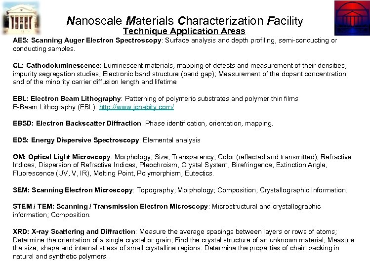 Nanoscale Materials Characterization Facility Technique Application Areas AES: Scanning Auger Electron Spectroscopy: Surface analysis and depth profiling, semi-conducting or conducting samples. CL: Cathodoluminescence: Luminescent materials, mapping of defects and measurement of their densities, impurity segregation studies; Electronic band structure (band gap); Measurement of the dopant concentration and of the minority carrier diffusion length and lifetime EBL: Electron Beam Lithography: Patterning of polymeric substrates and polymer thin films E-Beam Lithography (EBL): http: //www. jcnabity. com/ EBSD: Electron Backscatter Diffraction: Phase identification, orientation, mapping. EDS: Energy Dispersive Spectroscopy: Elemental analysis OM: Optical Light Microscopy: Morphology; Size; Transparency; Color (reflected and transmitted), Refractive Indices, Dispersion of Refractive Indices, Pleochroism, Crystal System, Birefringence, Extinction Angle, Fluorescence (UV, V, IR), Melting Point, Polymorphism, Eutectics. SEM: Scanning Electron Microscopy: Topography; Morphology; Composition; Crystallographic Information. STEM / TEM: Scanning / Transmission Electron Microscopy: Microstructural and crystallographic information; Composition. XRD: X-ray Scattering and Diffraction: Measure the average spacings between layers or rows of atoms; Determine the orientation of a single crystal or grain; Find the crystal structure of an unknown material; Measure the size, shape and internal stress of small crystalline regions. Determine the properties of chain packing in natural and synthetic polymers.
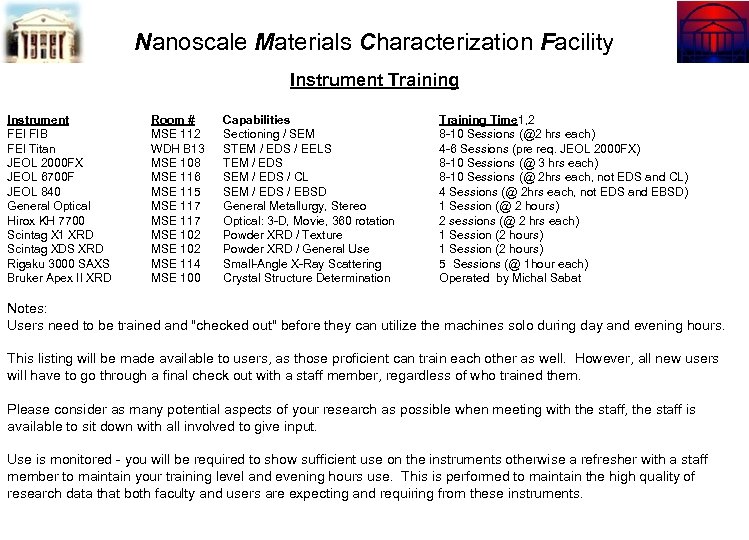 Nanoscale Materials Characterization Facility Instrument Training Instrument FEI FIB FEI Titan JEOL 2000 FX JEOL 6700 F JEOL 840 General Optical Hirox KH 7700 Scintag X 1 XRD Scintag XDS XRD Rigaku 3000 SAXS Bruker Apex II XRD Room # MSE 112 WDH B 13 MSE 108 MSE 116 MSE 115 MSE 117 MSE 102 MSE 114 MSE 100 Capabilities Sectioning / SEM STEM / EDS / EELS TEM / EDS SEM / EDS / CL SEM / EDS / EBSD General Metallurgy, Stereo Optical: 3 -D, Movie, 360 rotation Powder XRD / Texture Powder XRD / General Use Small-Angle X-Ray Scattering Crystal Structure Determination Training Time 1, 2 8 -10 Sessions (@2 hrs each) 4 -6 Sessions (pre req. JEOL 2000 FX) 8 -10 Sessions (@ 3 hrs each) 8 -10 Sessions (@ 2 hrs each, not EDS and CL) 4 Sessions (@ 2 hrs each, not EDS and EBSD) 1 Session (@ 2 hours) 2 sessions (@ 2 hrs each) 1 Session (2 hours) 5 Sessions (@ 1 hour each) Operated by Michal Sabat Notes: Users need to be trained and "checked out" before they can utilize the machines solo during day and evening hours. This listing will be made available to users, as those proficient can train each other as well. However, all new users will have to go through a final check out with a staff member, regardless of who trained them. Please consider as many potential aspects of your research as possible when meeting with the staff, the staff is available to sit down with all involved to give input. Use is monitored - you will be required to show sufficient use on the instruments otherwise a refresher with a staff member to maintain your training level and evening hours use. This is performed to maintain the high quality of research data that both faculty and users are expecting and requiring from these instruments.
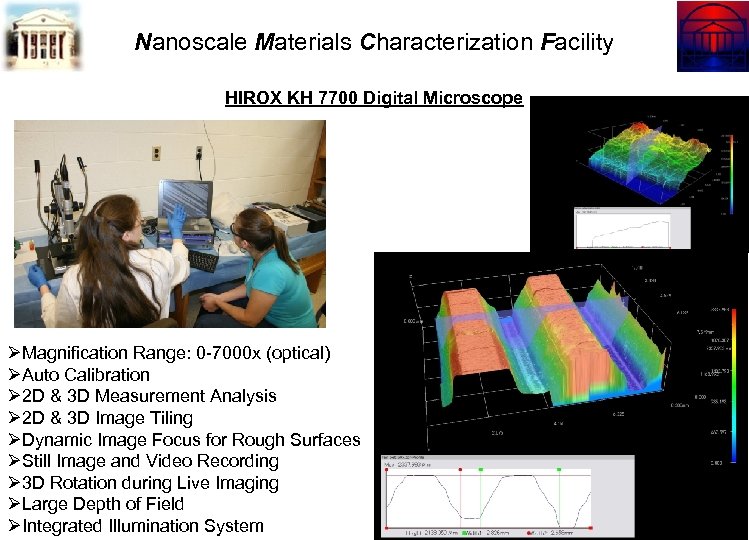 Nanoscale Materials Characterization Facility HIROX KH 7700 Digital Microscope ØMagnification Range: 0 -7000 x (optical) ØAuto Calibration Ø 2 D & 3 D Measurement Analysis Ø 2 D & 3 D Image Tiling ØDynamic Image Focus for Rough Surfaces ØStill Image and Video Recording Ø 3 D Rotation during Live Imaging ØLarge Depth of Field ØIntegrated Illumination System
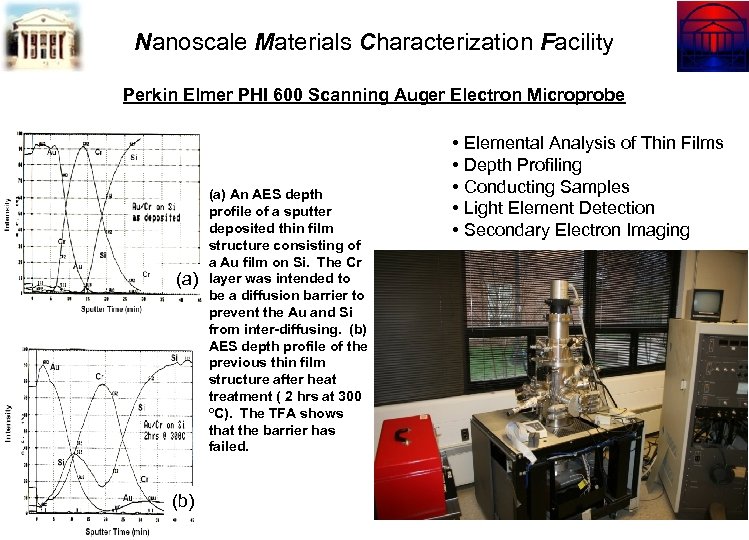 Nanoscale Materials Characterization Facility Perkin Elmer PHI 600 Scanning Auger Electron Microprobe (a) (b) (a) An AES depth profile of a sputter deposited thin film structure consisting of a Au film on Si. The Cr layer was intended to be a diffusion barrier to prevent the Au and Si from inter-diffusing. (b) AES depth profile of the previous thin film structure after heat treatment ( 2 hrs at 300 ºC). The TFA shows that the barrier has failed. • Elemental Analysis of Thin Films • Depth Profiling • Conducting Samples • Light Element Detection • Secondary Electron Imaging
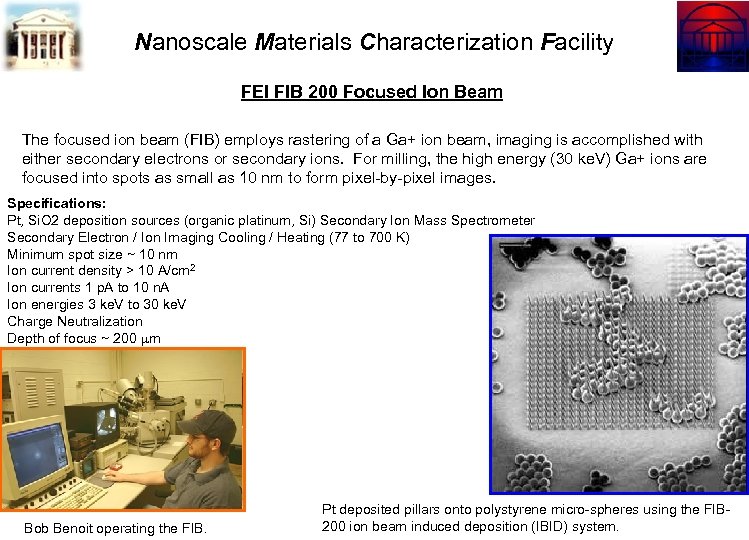 Nanoscale Materials Characterization Facility FEI FIB 200 Focused Ion Beam The focused ion beam (FIB) employs rastering of a Ga+ ion beam, imaging is accomplished with either secondary electrons or secondary ions. For milling, the high energy (30 ke. V) Ga+ ions are focused into spots as small as 10 nm to form pixel-by-pixel images. Specifications: Pt, Si. O 2 deposition sources (organic platinum, Si) Secondary Ion Mass Spectrometer Secondary Electron / Ion Imaging Cooling / Heating (77 to 700 K) Minimum spot size ~ 10 nm Ion current density > 10 A/cm 2 Ion currents 1 p. A to 10 n. A Ion energies 3 ke. V to 30 ke. V Charge Neutralization Depth of focus ~ 200 m Bob Benoit operating the FIB. Pt deposited pillars onto polystyrene micro-spheres using the FIB 200 ion beam induced deposition (IBID) system.
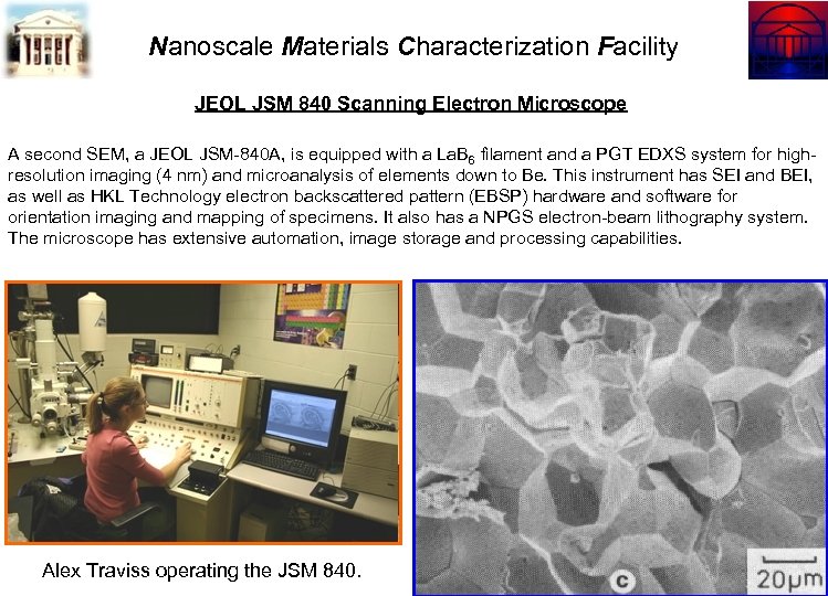 Nanoscale Materials Characterization Facility JEOL JSM 840 Scanning Electron Microscope A second SEM, a JEOL JSM-840 A, is equipped with a La. B 6 filament and a PGT EDXS system for highresolution imaging (4 nm) and microanalysis of elements down to Be. This instrument has SEI and BEI, as well as HKL Technology electron backscattered pattern (EBSP) hardware and software for orientation imaging and mapping of specimens. It also has a NPGS electron-beam lithography system. The microscope has extensive automation, image storage and processing capabilities. Alex Traviss operating the JSM 840.
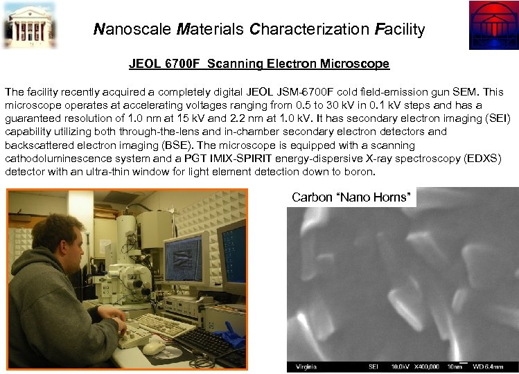 Nanoscale Materials Characterization Facility JEOL 6700 F Scanning Electron Microscope The facility recently acquired a completely digital JEOL JSM-6700 F cold field-emission gun SEM. This microscope operates at accelerating voltages ranging from 0. 5 to 30 k. V in 0. 1 k. V steps and has a guaranteed resolution of 1. 0 nm at 15 k. V and 2. 2 nm at 1. 0 k. V. It has secondary electron imaging (SEI) capability utilizing both through-the-lens and in-chamber secondary electron detectors and backscattered electron imaging (BSE). The microscope is equipped with a scanning cathodoluminescence system and a PGT IMIX-SPIRIT energy-dispersive X-ray spectroscopy (EDXS) detector with an ultra-thin window for light element detection down to boron. Carbon “Nano Horns”
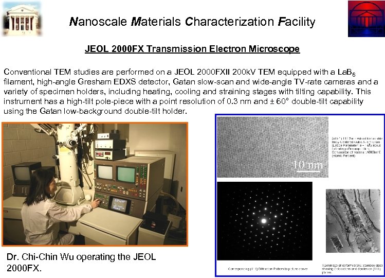 Nanoscale Materials Characterization Facility JEOL 2000 FX Transmission Electron Microscope Conventional TEM studies are performed on a JEOL 2000 FXII 200 k. V TEM equipped with a La. B 6 filament, high-angle Gresham EDXS detector, Gatan slow-scan and wide-angle TV-rate cameras and a variety of specimen holders, including heating, cooling and straining stages with tilting capability. This instrument has a high-tilt pole-piece with a point resolution of 0. 3 nm and ± 60° double-tilt capability using the Gatan low-background double-tilt holder. Dr. Chi-Chin Wu operating the JEOL 2000 FX.
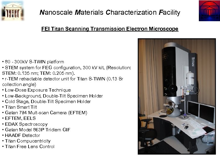 Nanoscale Materials Characterization Facility FEI Titan Scanning Transmission Electron Microscope • 80 - 300 k. V S-TWIN platform • STEM system for FEG configuration, 300 k. V kit, (Resolution: STEM: 0. 135 nm; TEM: 0. 205 nm). • r-TEM retractable detector unit for Titan S-TWIN (0. 13 Sr collection angle) • Low-Dose Exposure Technique • Low-Background, Double-Tilt Specimen Holder • Cold Stage, Double-Tilt Specimen Holder • Titan Smart Tilt • Gatan 794 Mult-scan Camera (EFTEM) • EFTEM, EELS • EDAX Spectroscopy • Gatan Model 863 P Tridiem GIF • HAADF Detector • Titan Compucentricity • Titan Free Lens Control
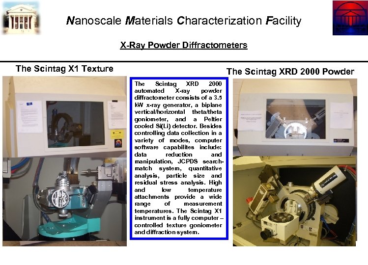 Nanoscale Materials Characterization Facility X-Ray Powder Diffractometers The Scintag X 1 Texture The Scintag XRD 2000 Powder The Scintag XRD 2000 automated X-ray powder diffractometer consists of a 3. 5 k. W x-ray generator, a biplane vertical/horizontal theta/theta goniometer, and a Peltier cooled Si(Li) detector. Besides controlling data collection in a variety of modes, computer software capabilites include: data reduction and manipulation, JCPDS searchmatch system, quantitative analysis, particle size and residual stress analysis. High and low temperature attachments provide a wide range of measurement temperatures. The Scintag X 1 instrument is a fully computer – controlled texture goniometer and diffraction system.
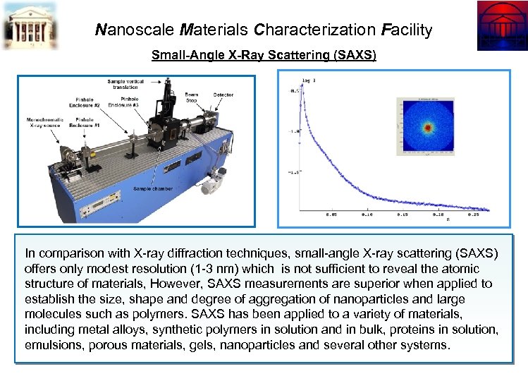 Nanoscale Materials Characterization Facility Small-Angle X-Ray Scattering (SAXS) In comparison with X-ray diffraction techniques, small-angle X-ray scattering (SAXS) offers only modest resolution (1 -3 nm) which is not sufficient to reveal the atomic structure of materials, However, SAXS measurements are superior when applied to establish the size, shape and degree of aggregation of nanoparticles and large molecules such as polymers. SAXS has been applied to a variety of materials, including metal alloys, synthetic polymers in solution and in bulk, proteins in solution, emulsions, porous materials, gels, nanoparticles and several other systems.
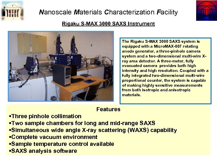 Nanoscale Materials Characterization Facility Rigaku S-MAX 3000 SAXS Instrument The Rigaku S-MAX 3000 SAXS system is equipped with a Micro. MAX-007 rotating anode generator, a three-pinhole camera system and a two-dimensional multi-wire Xray area detector. A three-meter, fully evacuated camera provides both high intensity and high resolution. Coupled with a fully integrated two-dimensional multi-wire proportional counter, the system is capable of making highly sensitive measurements from both isotropic and anisotropic materials. Features §Three pinhole collimation §Two sample chambers for long and mid-range SAXS §Simultaneous wide angle X-ray scattering (WAXS) capability §Complete vacuum environment §Sample temperature control available §SAXS analysis software
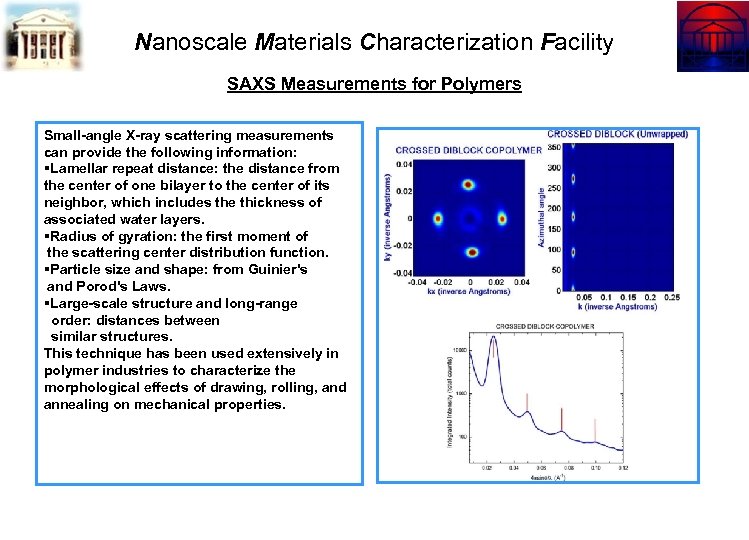 Nanoscale Materials Characterization Facility SAXS Measurements for Polymers Small-angle X-ray scattering measurements can provide the following information: §Lamellar repeat distance: the distance from the center of one bilayer to the center of its neighbor, which includes the thickness of associated water layers. §Radius of gyration: the first moment of the scattering center distribution function. §Particle size and shape: from Guinier's and Porod's Laws. §Large-scale structure and long-range order: distances between similar structures. This technique has been used extensively in polymer industries to characterize the morphological effects of drawing, rolling, and annealing on mechanical properties.
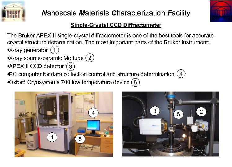 Nanoscale Materials Characterization Facility Single-Crystal CCD Diffractometer The Bruker APEX II single-crystal diffractometer is one of the best tools for accurate crystal structure determination. The most important parts of the Bruker instrument: • X-ray generator 1 • X-ray source-ceramic Mo tube 2 • APEX II CCD detector 3 • PC computer for data collection control and structure determination 4 • Oxford Cryosystems 700 low temperature device 5 4 1 5 3 5 2
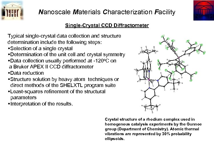 Nanoscale Materials Characterization Facility Single-Crystal CCD Diffractometer Typical single-crystal data collection and structure determination include the following steps: §Selection of a single crystal §Determination of the unit cell and crystal symmetry §Data collection usually performed at -120 o. C on a Bruker APEX II CCD diffractometer §Data reduction §Structure solution by heavy atom techniques or direct methods of the SHELXTL program suite §Least-squares refinement of the structural parameters §Interpretation of the results. Crystal structure of a rhodium complex used in homogenous catalysis experiments by the Gunnoe group (Department of Chemistry). Atomic thermal vibrations are represented by 30% probability ellipsoids.
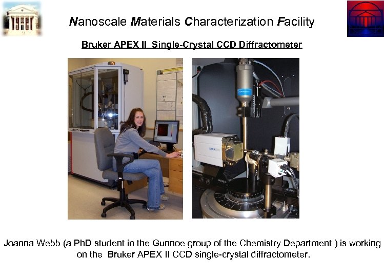 Nanoscale Materials Characterization Facility Bruker APEX II Single-Crystal CCD Diffractometer Joanna Webb (a Ph. D student in the Gunnoe group of the Chemistry Department ) is working on the Bruker APEX II CCD single-crystal diffractometer.
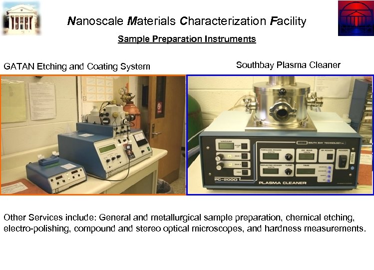 Nanoscale Materials Characterization Facility Sample Preparation Instruments GATAN Etching and Coating System Southbay Plasma Cleaner Other Services include: General and metallurgical sample preparation, chemical etching, electro-polishing, compound and stereo optical microscopes, and hardness measurements.
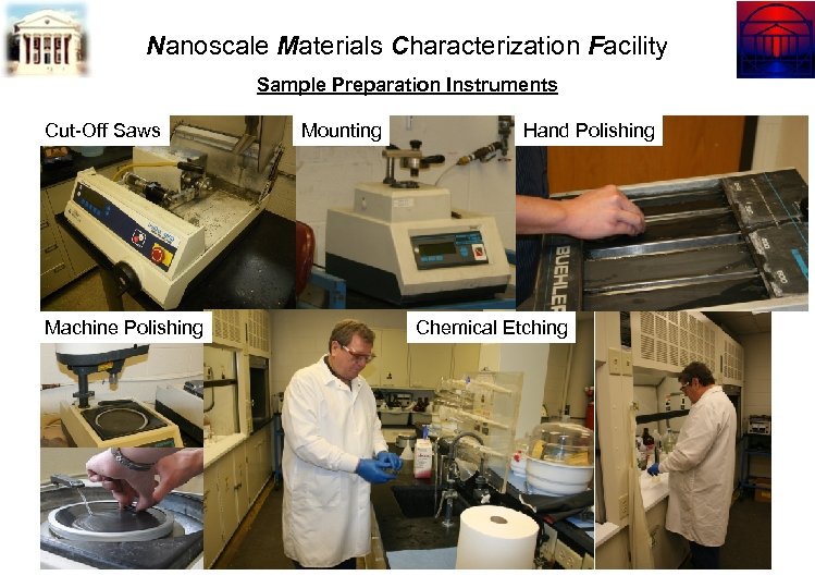 Nanoscale Materials Characterization Facility Sample Preparation Instruments Cut-Off Saws Machine Polishing Mounting Hand Polishing Chemical Etching
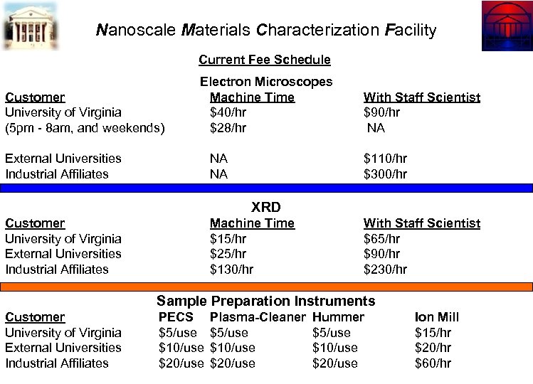 Nanoscale Materials Characterization Facility Current Fee Schedule Customer University of Virginia (5 pm - 8 am, and weekends) Electron Microscopes Machine Time $40/hr $28/hr External Universities Industrial Affiliates NA NA With Staff Scientist $90/hr NA $110/hr $300/hr XRD Customer University of Virginia External Universities Industrial Affiliates Machine Time $15/hr $25/hr $130/hr With Staff Scientist $65/hr $90/hr $230/hr Sample Preparation Instruments Customer University of Virginia External Universities Industrial Affiliates PECS $5/use $10/use $20/use Plasma-Cleaner $5/use $10/use $20/use Hummer $5/use $10/use $20/use Ion Mill $15/hr $20/hr $60/hr


