58eaa733b9b799c7273b324887bb5caa.ppt
- Количество слайдов: 76
Nanoscale Device Modelling: CMOS and beyond G. Iannaccone Università di Pisa and IU. NET [Italian Universities Nanoelectronics Consortium] Via Caruso 16, I-56122, Pisa, Italy. g. iannaccone@iet. unipi. it G. Iannaccone Università di Pisa
Acknowledgments n People that did (are doing) the “real” work w A. Campera, P. Coli, G. Curatola, G. Fiori, F. Crupi, G. Mugnaini, A. Nannipieri, F. Nardi, M. Pala, L. Perniola n Partners w IMEC, LETI, STM, Silvaco (EU Fin. Flash Project) w Univ. Wuerzburg, ETH Zurich, TU Vienna, MPG Stuttgart, NMRC Cork (EU Nano. TCAD Project) w EU Sinano No. E (43 partners) Next: Pull. NANO IP w IU. NET Italian Universities Nanoelectronics Corsortium w Univ. Bologna, Univ. Udine, Univ. Roma (PRIN Programme) w Philips Research Leuven, Purdue University, Univ. Illinois at Urbana Champaign, Samsung n Funding (past and present) w European Commission, Italian Ministry of University, Italian National Research Council, Foundation of Pisa Savings Bank, Silvaco International G. Iannaccone Università di Pisa
The Problem “Yesterday’s technology modeled tomorrow” (M. E. Law, 2004) TCAD and numerical modeling tools – both for process and device simulation – are accurate, or “predictive”, only for a sufficiently stable and “mature” technology, and after a lengthy calibration procedure. G. Iannaccone Università di Pisa

Modeling as a Strategic Activity Modeling is a strategic activity because it enables to early evaluation of technology options make choices and cut unpromising initiatives strategically position and focus R&D efforts n perform an n n Modeling supports the definition and the implementation of a R&D strategy G. Iannaccone Università di Pisa
Present activity in Pisa ITRS Roadmap Issues n Quantum ballistic and quasiballistic modeling of nanoscale MOSFETs (2 D-3 D) n Alternative device structures (DG MOSFETs, FINFETs, SNWTs) n Tunneling currents through oxides and high-k gate stacks, also in the presence of defects (SILCs, etc. ) n Atomistic effects in nanoscale MOSFETs n Compact modeling of nanoscale MOSFETs G. Iannaccone Emerging Research Devices n Nanocrystal and discrete trap flash memories n Quantum dots and single electron transistors n CNT-FETs n Resonant Tunneling Devices Fundamentals of Nanoelectronics n Decoherence and dephasing n Spin-dependent transport n Mesoscopic transport Università di Pisa
Present activity in Pisa ITRS Roadmap Issues n Quantum ballistic and quasiballistic modeling of nanoscale MOSFETs (2 D-3 D) n Alternative device structures (DG MOSFETs, FINFETs, SNWTs) n Tunneling currents through oxides and high-k gate stacks, also in the presence of defects (SILCs, etc. ) n Atomistic effects in nanoscale MOSFETs n Compact modeling of nanoscale MOSFETs G. Iannaccone Emerging Research Devices n Nanocrystal and discrete trap flash memories n Quantum dots and single electron transistors n CNT-FETs n Resonant Tunneling Devices Fundamentals of Nanoelectronics n Decoherence and dephasing n Spin-dependent transport n Mesoscopic transport Università di Pisa
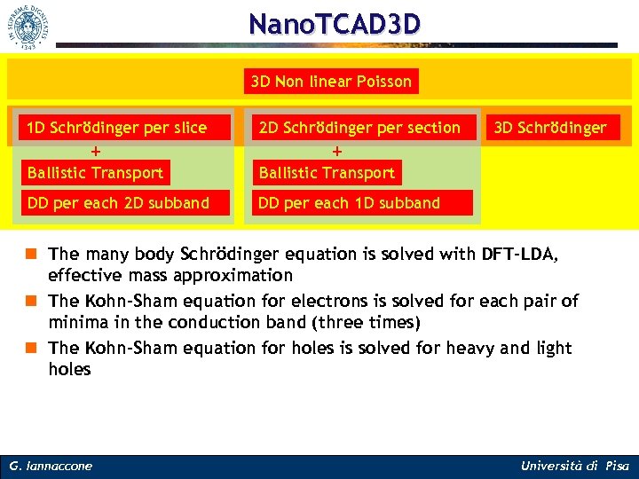
Nano. TCAD 3 D 3 D Non linear Poisson 1 D Schrödinger per slice + 2 D Schrödinger per section 3 D Schrödinger + Ballistic Transport DD per each 2 D subband DD per each 1 D subband n The many body Schrödinger equation is solved with DFT-LDA, effective mass approximation n The Kohn-Sham equation for electrons is solved for each pair of minima in the conduction band (three times) n The Kohn-Sham equation for holes is solved for heavy and light holes G. Iannaccone Università di Pisa
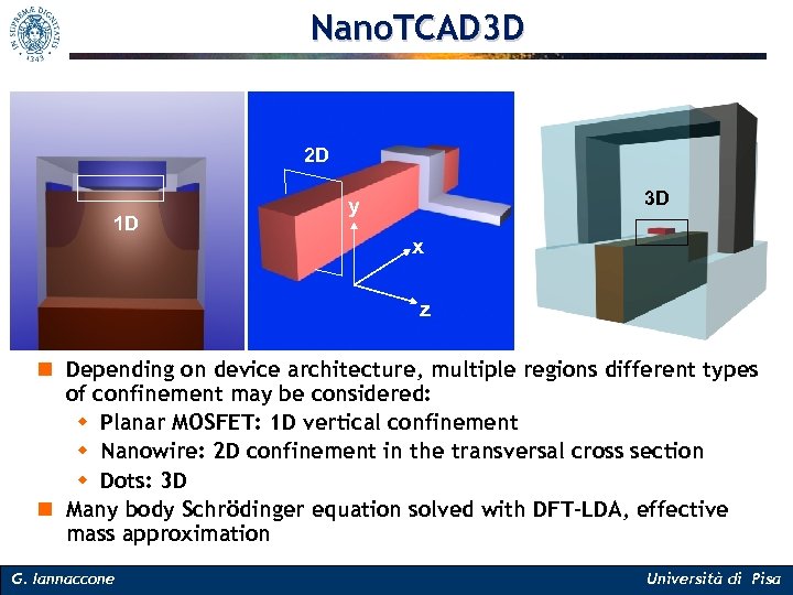
Nano. TCAD 3 D 2 D 1 D 3 D y x z n Depending on device architecture, multiple regions different types of confinement may be considered: w Planar MOSFET: 1 D vertical confinement w Nanowire: 2 D confinement in the transversal cross section w Dots: 3 D n Many body Schrödinger equation solved with DFT-LDA, effective mass approximation G. Iannaccone Università di Pisa
Quantum ballistic and quasiballistic modeling of nanoscale MOSFETs (3 D) Lead: G. Fiori G. Iannaccone Università di Pisa
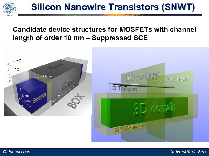
Silicon Nanowire Transistors (SNWT) Candidate device structures for MOSFETs with channel length of order 10 nm – Suppressed SCE G. Iannaccone Università di Pisa

Transport models in the 1 D subbands Two models for current 1. Ballistic transport in each subband (including tunneling) 2. Drift-Diffusion transport in each 1 D subband (Ei). (note: The mobility model must be improved). 1 D subband profiles 4 th The 3 D electron density is obtained as : 3 rd 2 nd 1 st G. Iannaccone Università di Pisa
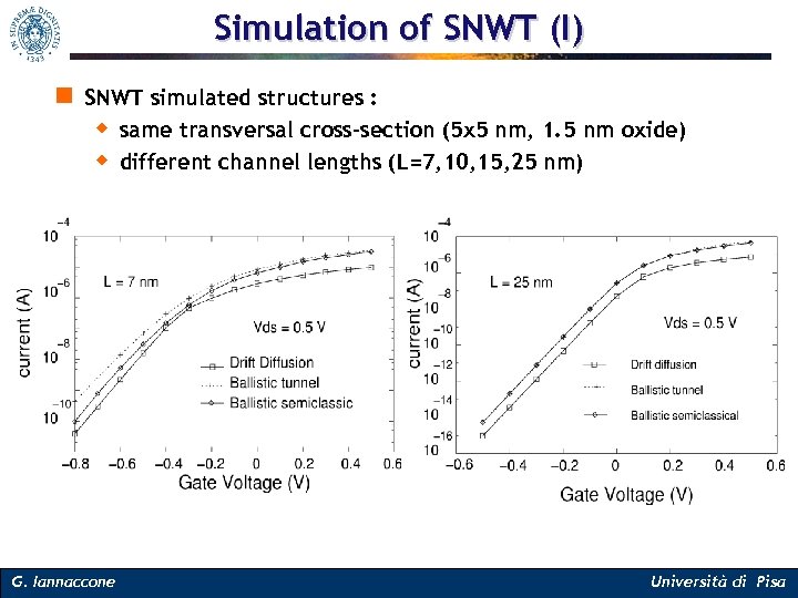
Simulation of SNWT (I) n SNWT simulated structures : w same transversal cross-section (5 x 5 nm, 1. 5 nm oxide) w different channel lengths (L=7, 10, 15, 25 nm) G. Iannaccone Università di Pisa
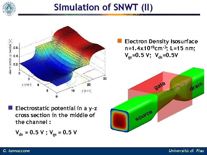
Simulation of SNWT (II) n Electron Density Isosurface n=1. 4 x 1019 cm-3; L=15 nm; Vgs=0. 5 V; Vds=0. 5 V ate g n Electrostatic potential in a y-z cross section in the middle of the channel : rai d n rce ou s Vds = 0. 5 V ; Vgs = 0. 5 V G. Iannaccone Università di Pisa
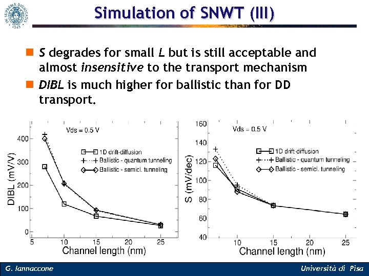
Simulation of SNWT (III) n S degrades for small L but is still acceptable and almost insensitive to the transport mechanism n DIBL is much higher for ballistic than for DD transport. G. Iannaccone Università di Pisa
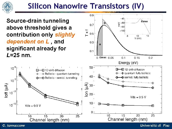
Silicon Nanowire Transistors (IV) Source-drain tunneling above threshold gives a contribution only slightly dependent on L , and significant already for L=25 nm. G. Iannaccone Università di Pisa
High-k dielectrics Lead: Andrea Campera G. Iannaccone Università di Pisa
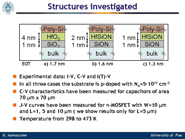
Structures investigated 4 nm 1 nm Poly-Si Hf. O 2 Si. O 2 bulk EOT a) 1. 7 nm Poly-Si 2 nm Hf. Si. ON 1 nm Si. ON bulk Poly-Si 1 nm Hf. Si. ON 1 nm Si. ON bulk b) 1. 6 nm c) 1. 3 nm n Experimental data: I-V, C-V and I(T)-V n In all three cases the substrate is p-doped with NA=5∙ 1017 cm-3 n C-V characteristics have been measured for capacitors of area 70 µm x 70 µm n J-V curves have been measured for n-MOSFET with W=10 µm and L=1, 5 and 10 µm ( we show results only for L=5 µm) n Temperature from 298 to 473 K G. Iannaccone Università di Pisa
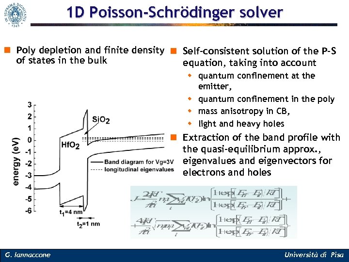
1 D Poisson-Schrödinger solver n Poly depletion and finite density n Self-consistent solution of the P-S of states in the bulk equation, taking into account w quantum confinement at the emitter, w quantum confinement in the poly w mass anisotropy in CB, w light and heavy holes n Extraction of the band profile with the quasi-equilibrium approx. , eigenvalues and eigenvectors for electrons and holes G. Iannaccone Università di Pisa
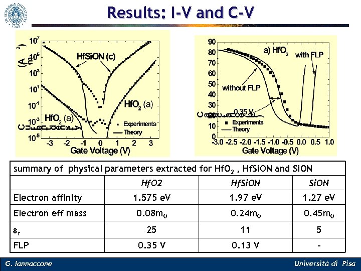
Results: I-V and C-V summary of physical parameters extracted for Hf. O 2 , Hf. Si. ON and Si. ON Hf. O 2 Hf. Si. ON Electron affinity 1. 575 e. V 1. 97 e. V 1. 27 e. V Electron eff mass 0. 08 m 0 0. 24 m 0 0. 45 m 0 25 11 5 0. 35 V 0. 13 V - er FLP G. Iannaccone Università di Pisa
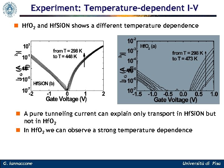
Experiment: Temperature-dependent I-V n Hf. O 2 and Hf. Si. ON shows a different temperature dependence n A pure tunneling current can explain only transport in Hf. Si. ON but not in Hf. O 2 n In Hf. O 2 we can observe a strong temperature dependence G. Iannaccone Università di Pisa
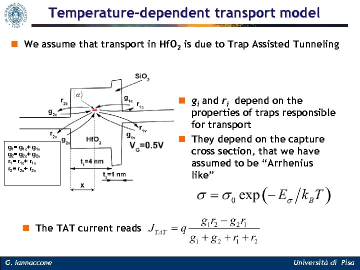
Temperature-dependent transport model n We assume that transport in Hf. O 2 is due to Trap Assisted Tunneling g 1= g 1 c+ g 1 v g 2= g 2 c+ g 2 v r 1= r 1 c+ r 1 v r 2= r 2 c+ r 2 v n gi and ri depend on the properties of traps responsible for transport n They depend on the capture cross section, that we have assumed to be “Arrhenius like” n The TAT current reads G. Iannaccone Università di Pisa
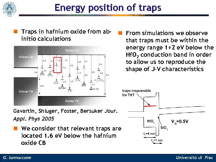
Energy position of traps n Traps in hafnium oxide from ab- n From simulations we observe initio calculations that traps must be within the energy range 1÷ 2 e. V below the Hf. O 2 conduction band in order to allow us to reproduce the shape of J-V characteristics Gavartin, Shluger, Foster, Bersuker Jour. Appl. Phys 2005 n We consider that relevant traps are located 1. 6 e. V below the hafnium oxide CB G. Iannaccone Università di Pisa
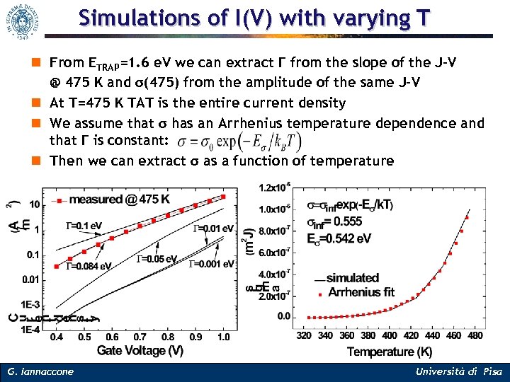
Simulations of I(V) with varying T n From ETRAP=1. 6 e. V we can extract Г from the slope of the J-V @ 475 K and σ(475) from the amplitude of the same J-V n At T=475 K TAT is the entire current density n We assume that σ has an Arrhenius temperature dependence and that Г is constant: n Then we can extract σ as a function of temperature G. Iannaccone Università di Pisa
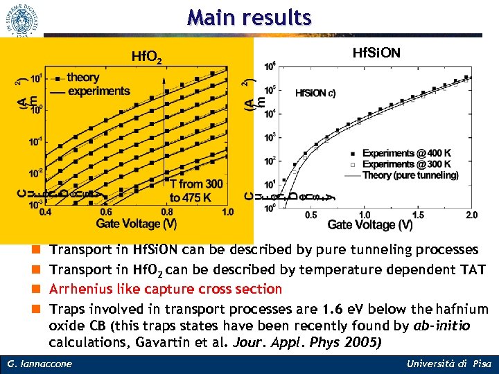
Main results Hf. O 2 n n Hf. Si. ON Transport in Hf. Si. ON can be described by pure tunneling processes Transport in Hf. O 2 can be described by temperature dependent TAT Arrhenius like capture cross section Traps involved in transport processes are 1. 6 e. V below the hafnium oxide CB (this traps states have been recently found by ab-initio calculations, Gavartin et al. Jour. Appl. Phys 2005) G. Iannaccone Università di Pisa
Decoherence and dephasing Lead: Marco Pala* M. Pala, G. Iannaccone, PRB vol. 69, 235304 (2004) M. Pala, G. Iannaccone, PRL vol. 93, 256803 (2004) * now with IMEP-CNRS, Grenoble G. Iannaccone Università di Pisa
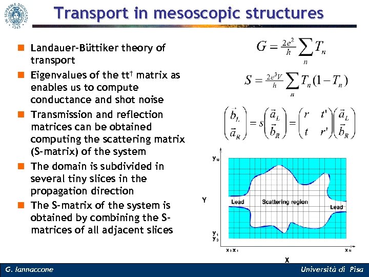
Transport in mesoscopic structures n Landauer-Büttiker theory of transport n Eigenvalues of the tt† matrix as enables us to compute conductance and shot noise n Transmission and reflection matrices can be obtained computing the scattering matrix (S-matrix) of the system n The domain is subdivided in several tiny slices in the propagation direction n The S-matrix of the system is obtained by combining the Smatrices of all adjacent slices G. Iannaccone Università di Pisa
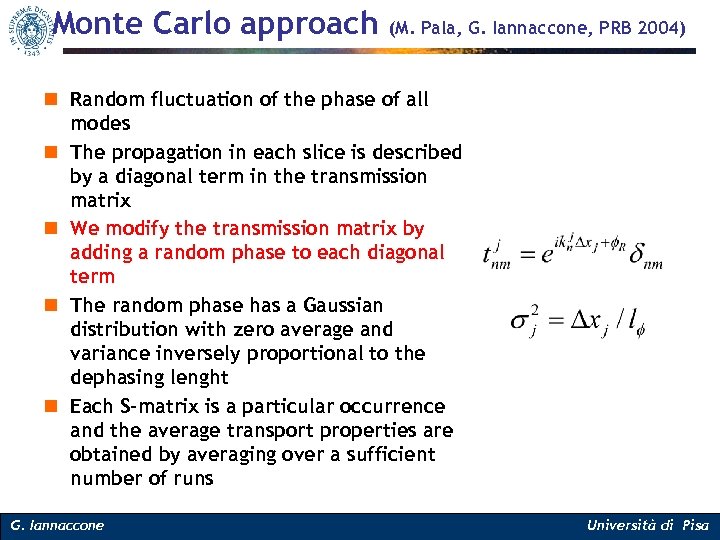
Monte Carlo approach (M. Pala, G. Iannaccone, PRB 2004) n Random fluctuation of the phase of all modes n The propagation in each slice is described by a diagonal term in the transmission matrix n We modify the transmission matrix by adding a random phase to each diagonal term n The random phase has a Gaussian distribution with zero average and variance inversely proportional to the dephasing lenght n Each S-matrix is a particular occurrence and the average transport properties are obtained by averaging over a sufficient number of runs G. Iannaccone Università di Pisa
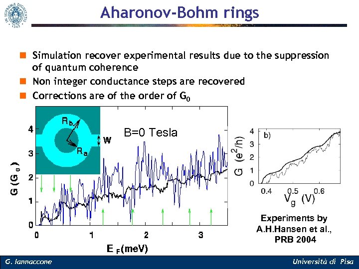
Aharonov-Bohm rings n Simulation recover experimental results due to the suppression of quantum coherence n Non integer conductance steps are recovered n Corrections are of the order of G 0 B=0 Tesla Experiments by A. H. Hansen et al. , PRB 2004 G. Iannaccone Università di Pisa
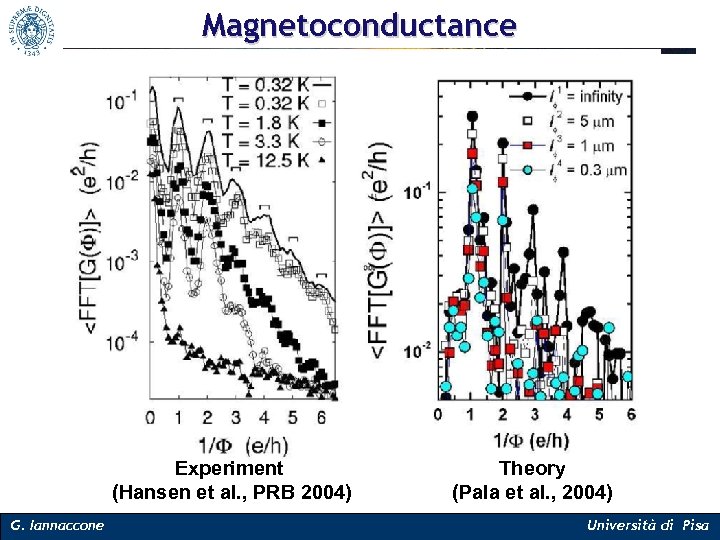
Magnetoconductance Experiment (Hansen et al. , PRB 2004) G. Iannaccone Theory (Pala et al. , 2004) Università di Pisa
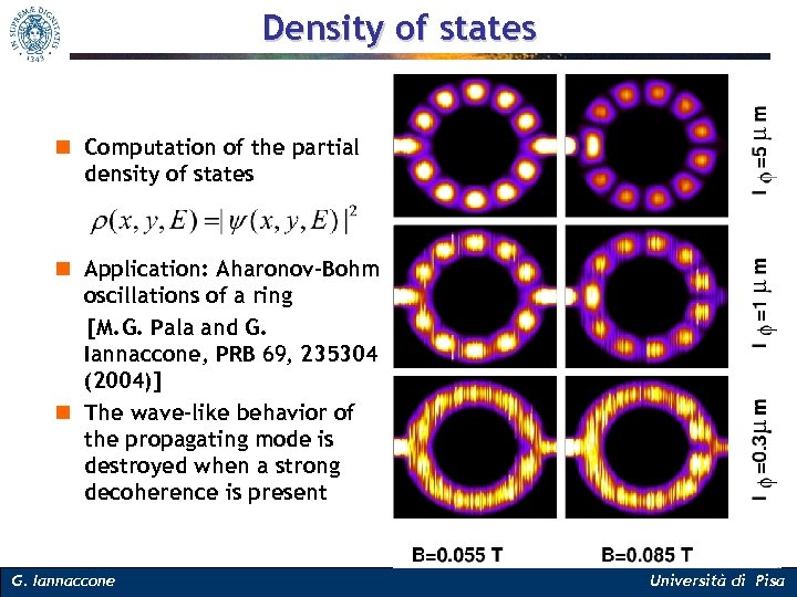
Density of states n Computation of the partial density of states n Application: Aharonov-Bohm oscillations of a ring [M. G. Pala and G. Iannaccone, PRB 69, 235304 (2004)] n The wave-like behavior of the propagating mode is destroyed when a strong decoherence is present G. Iannaccone Università di Pisa
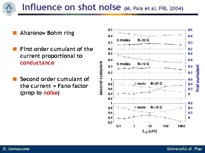
Influence on shot noise (M. Pala et al. PRL 2004) n Aharonov Bohm ring n First order cumulant of the current proportional to conductance n Second order cumulant of the current = Fano factor (prop to noise) G. Iannaccone Università di Pisa
Perspectives of Carbon Nanotube Field Effect Transistors Lead: G. Fiori Collaboration with Purdue University, G. Fiori et al. , IEDM 2005 – to be published on IEEETED, new results at ESSDERC 2006 G. Iannaccone Università di Pisa
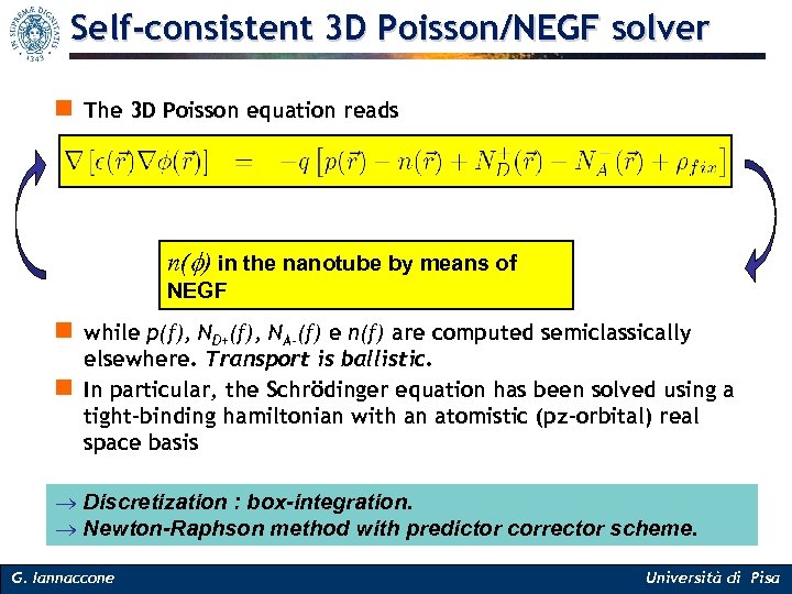
Self-consistent 3 D Poisson/NEGF solver n The 3 D Poisson equation reads n(f) in the nanotube by means of NEGF n while p(f), ND+(f), NA-(f) e n(f) are computed semiclassically n elsewhere. Transport is ballistic. In particular, the Schrödinger equation has been solved using a tight-binding hamiltonian with an atomistic (pz-orbital) real space basis ® Discretization : box-integration. ® Newton-Raphson method with predictor corrector scheme. G. Iannaccone Università di Pisa
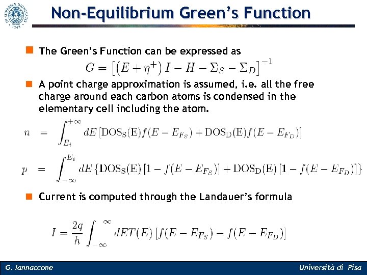
Non-Equilibrium Green’s Function n The Green’s Function can be expressed as n A point charge approximation is assumed, i. e. all the free charge around each carbon atoms is condensed in the elementary cell including the atom. n Current is computed through the Landauer’s formula G. Iannaccone Università di Pisa
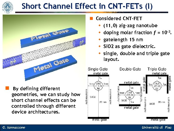
Short Channel Effect in CNT-FETs (I) n Considered CNT-FET w (11, 0) zig-zag nanotube w doping molar fraction f = 10 -3. w gatelength 15 nm w Si. O 2 as gate dielectric. w single, double and triple gate layout. n By defining different geometries, we can study how short channel effects can be controlled through different device architectures. G. Iannaccone Università di Pisa
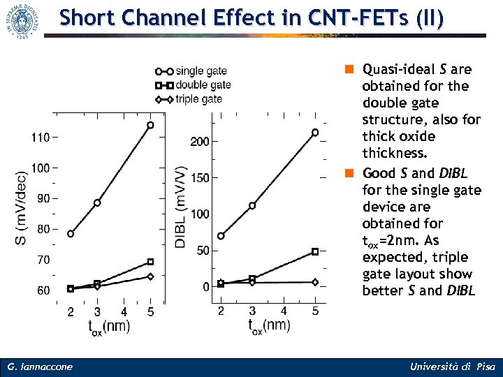
Short Channel Effect in CNT-FETs (II) n Quasi-ideal S are obtained for the double gate structure, also for thick oxide thickness. n Good S and DIBL for the single gate device are obtained for tox=2 nm. As expected, triple gate layout show better S and DIBL G. Iannaccone Università di Pisa
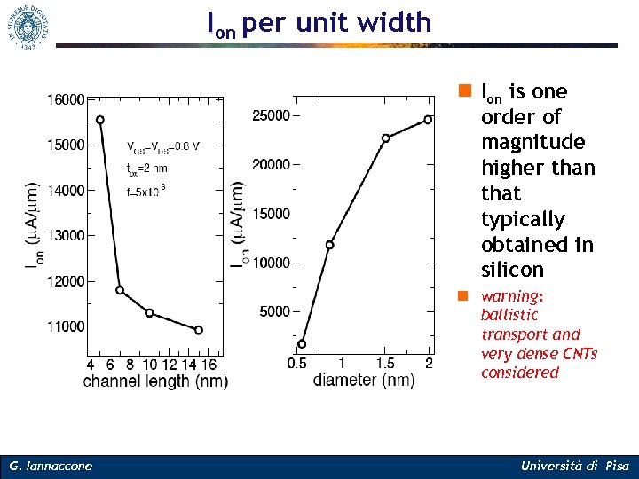
Ion per unit width n Ion is one order of magnitude higher than that typically obtained in silicon n warning: ballistic transport and very dense CNTs considered G. Iannaccone Università di Pisa
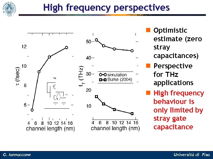
High frequency perspectives n Optimistic estimate (zero stray capacitances) n Perspective for THz applications n High frequency behaviour is only limited by stray gate capacitance G. Iannaccone Università di Pisa
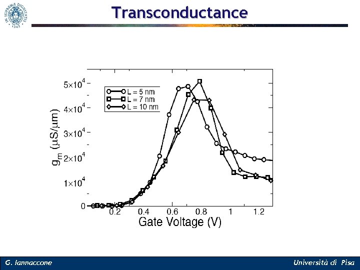
Transconductance G. Iannaccone Università di Pisa
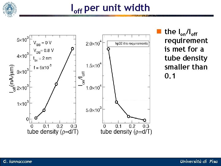
Ioff per unit width n the Ion/Ioff requirement is met for a tube density smaller than 0. 1 G. Iannaccone Università di Pisa
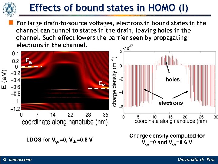
Effects of bound states in HOMO (I) n For large drain-to-source voltages, electrons in bound states in the channel can tunnel to states in the drain, leaving holes in the channel. Such effect lowers the barrier seen by propagating electrons in the channel. Efs Efd holes electrons LDOS for Vgs=0, Vds=0. 6 V G. Iannaccone Charge density computed for Vgs=0 and Vds=0. 6 V Università di Pisa
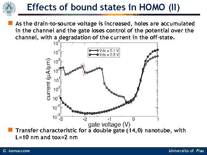
Effects of bound states in HOMO (II) n As the drain-to-source voltage is increased, holes are accumulated in the channel and the gate loses control of the potential over the channel, with a degradation of the current in the off-state. n Transfer characteristic for a double gate (14, 0) nanotube, with L=10 nm and tox=2 nm G. Iannaccone Università di Pisa

Work in Progress G. Iannaccone Università di Pisa
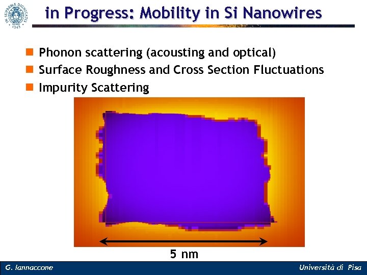
in Progress: Mobility in Si Nanowires n Phonon scattering (acousting and optical) n Surface Roughness and Cross Section Fluctuations n Impurity Scattering 5 nm G. Iannaccone Università di Pisa
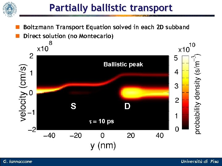
Partially ballistic transport n Boltzmann Transport Equation solved in each 2 D subband n Direct solution (no Montecarlo) Ballistic peak S D t = 10 ps G. Iannaccone Università di Pisa
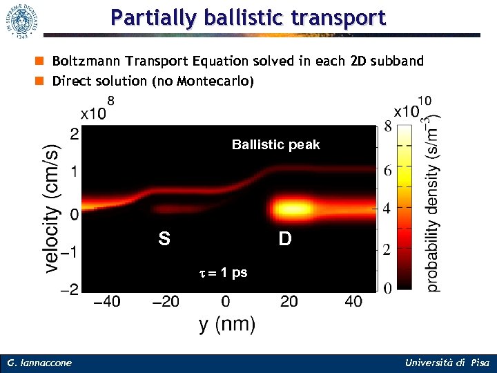
Partially ballistic transport n Boltzmann Transport Equation solved in each 2 D subband n Direct solution (no Montecarlo) Ballistic peak S D t = 1 ps G. Iannaccone Università di Pisa
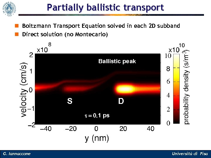
Partially ballistic transport n Boltzmann Transport Equation solved in each 2 D subband n Direct solution (no Montecarlo) Ballistic peak S D t = 0. 1 ps G. Iannaccone Università di Pisa
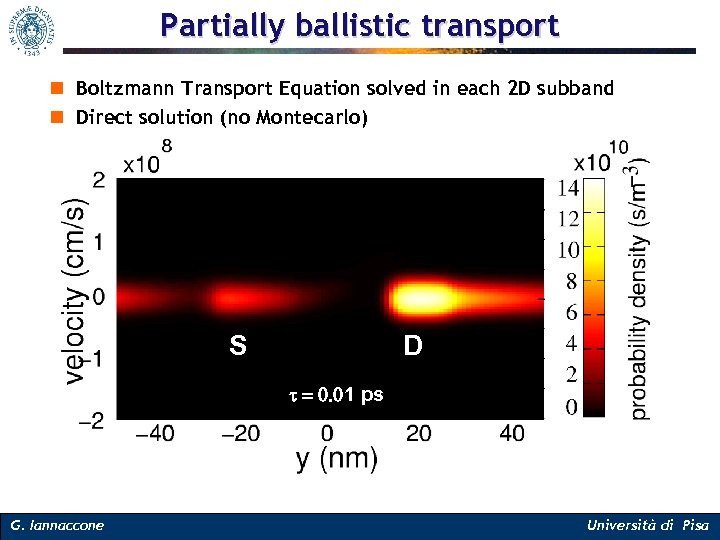
Partially ballistic transport n Boltzmann Transport Equation solved in each 2 D subband n Direct solution (no Montecarlo) S D t = 0. 01 ps G. Iannaccone Università di Pisa
Personal Conclusion n Critical objectives of nanoscale device modeling: w Provide useful insights of device behavior, w helping us to understand § what are the relevant physical aspects for the issues at hand § what are the main trends § what we should focus on and what we should stop. n Such mission does not requires huge do-it-all tools, but simulation tools with different degrees of sophistication, tailored to the particular problem at hand. G. Iannaccone Università di Pisa
Modeling of ballistic and quasi-ballistic MOSFETs Lead: G. Curatola* In collaboration with Philips Research Leuven, G. Curatola et al. IEEE-TED vol. 52, p. 1851 -1858, 2005 * now with Philips Research Leuven G. Iannaccone Università di Pisa
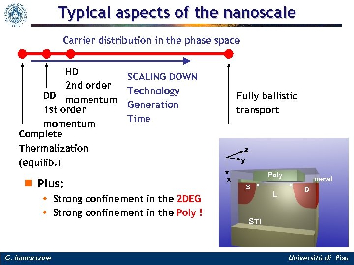
Typical aspects of the nanoscale Carrier distribution in the phase space HD 2 nd order DD momentum 1 st order momentum Complete Thermalization (equilib. ) SCALING DOWN Technology Generation Time n Plus: w Strong confinement in the 2 DEG w Strong confinement in the Poly ! G. Iannaccone Fully ballistic transport z y Poly x S L metal D STI Università di Pisa
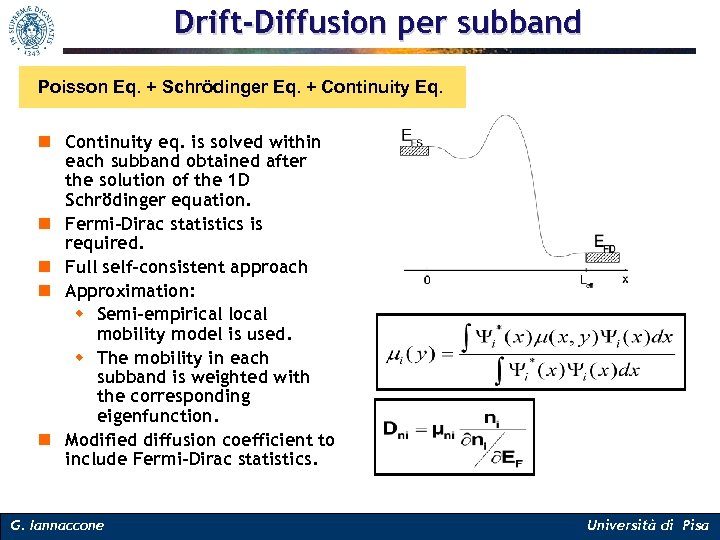
Drift-Diffusion per subband Poisson Eq. + Schrödinger Eq. + Continuity Eq. n Continuity eq. is solved within each subband obtained after the solution of the 1 D Schrödinger equation. n Fermi-Dirac statistics is required. n Full self-consistent approach n Approximation: w Semi-empirical local mobility model is used. w The mobility in each subband is weighted with the corresponding eigenfunction. n Modified diffusion coefficient to include Fermi-Dirac statistics. G. Iannaccone Università di Pisa
Bulk n. MOSFETs: Inverse Modelling n Data (PLI 1043 process) from Philips Research Leuven: w Doping profile obtained with TSUPREM 4 w Oxide thickness Tox=1. 5 nm w C-V and I-V characteristics w Set of devices with different gate length! n Several Unknowns: w Gate length (dispersion with respect to nominal value) w Channel doping w Polysilicon Doping w LDD, HDD, pocket implant doping G. Iannaccone Università di Pisa
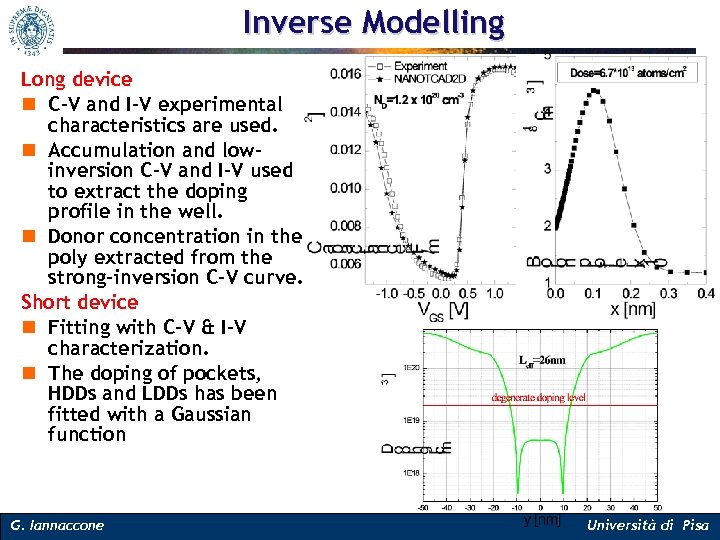
Inverse Modelling Long device n C-V and I-V experimental characteristics are used. n Accumulation and lowinversion C-V and I-V used to extract the doping profile in the well. n Donor concentration in the poly extracted from the strong-inversion C-V curve. Short device n Fitting with C-V & I-V characterization. n The doping of pockets, HDDs and LDDs has been fitted with a Gaussian function G. Iannaccone Università di Pisa
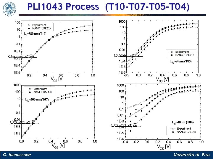
PLI 1043 Process (T 10 -T 07 -T 05 -T 04) G. Iannaccone Università di Pisa
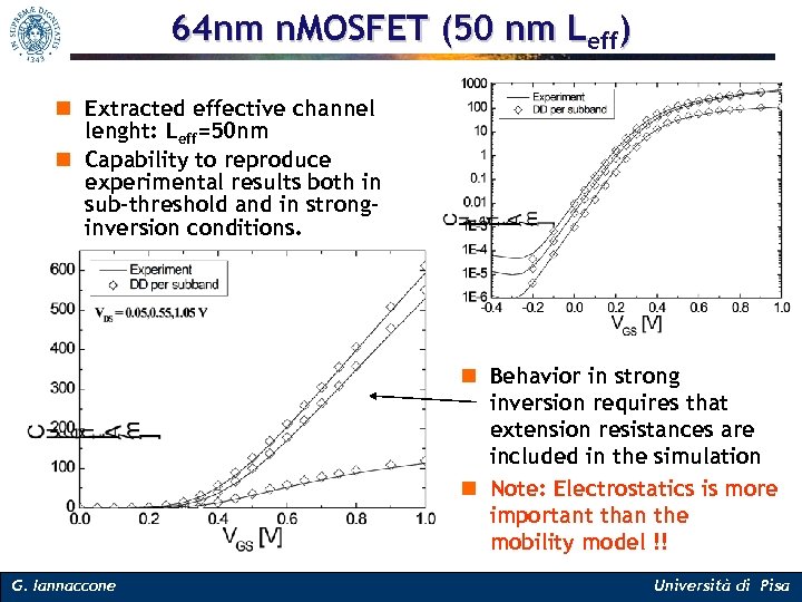
64 nm n. MOSFET (50 nm Leff) n Extracted effective channel lenght: Leff=50 nm n Capability to reproduce experimental results both in sub-threshold and in stronginversion conditions. n Behavior in strong inversion requires that extension resistances are included in the simulation n Note: Electrostatics is more important than the mobility model !! G. Iannaccone Università di Pisa
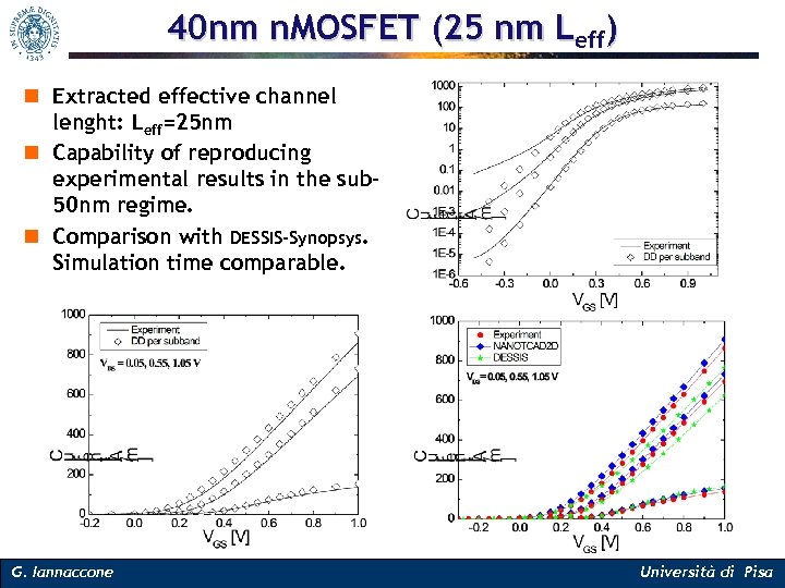
40 nm n. MOSFET (25 nm Leff) n Extracted effective channel lenght: Leff=25 nm n Capability of reproducing experimental results in the sub 50 nm regime. n Comparison with DESSIS-Synopsys. Simulation time comparable. G. Iannaccone Università di Pisa
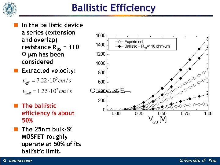
Ballistic Efficiency n In the ballistic device a series (extension and overlap) resistance RDS = 110 W m has been considered n Extracted velocity: n The ballistic efficiency is about 50% n The 25 nm bulk-Si MOSFET roughly operate at 50% of its ballistic limit. G. Iannaccone Università di Pisa
Nanocrystal and discrete-trap Flash memories Lead: G. Fiori et al. , APL, vol. 86, 113502 (2005) In collaboration with LETI, IMEC, STM (now in the Fin. Flash project) G. Iannaccone Università di Pisa
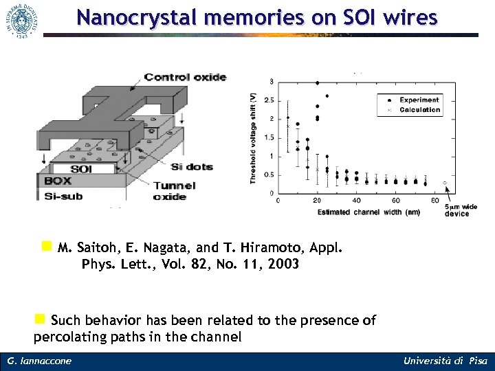
Nanocrystal memories on SOI wires n M. Saitoh, E. Nagata, and T. Hiramoto, Appl. Phys. Lett. , Vol. 82, No. 11, 2003 n Such behavior has been related to the presence of percolating paths in the channel G. Iannaccone Università di Pisa
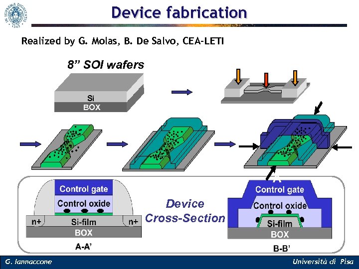
Device fabrication Realized by G. Molas, B. De Salvo, CEA-LETI 8” SOI wafers DUV E-beam DUV Si BOX A’ B B’ A Device Cross-Section G. Iannaccone Università di Pisa
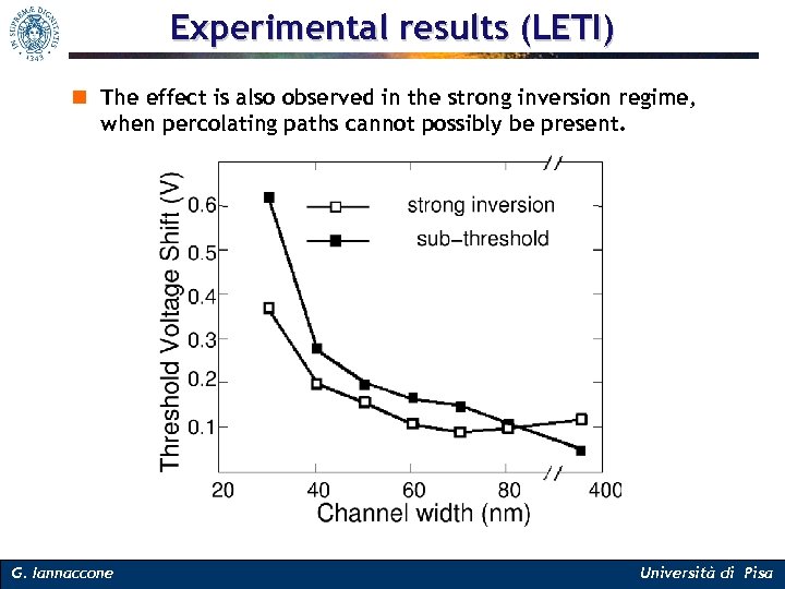
Experimental results (LETI) n The effect is also observed in the strong inversion regime, when percolating paths cannot possibly be present. G. Iannaccone Università di Pisa
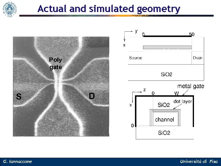
Actual and simulated geometry Poly gate S S G. Iannaccone W D D Università di Pisa
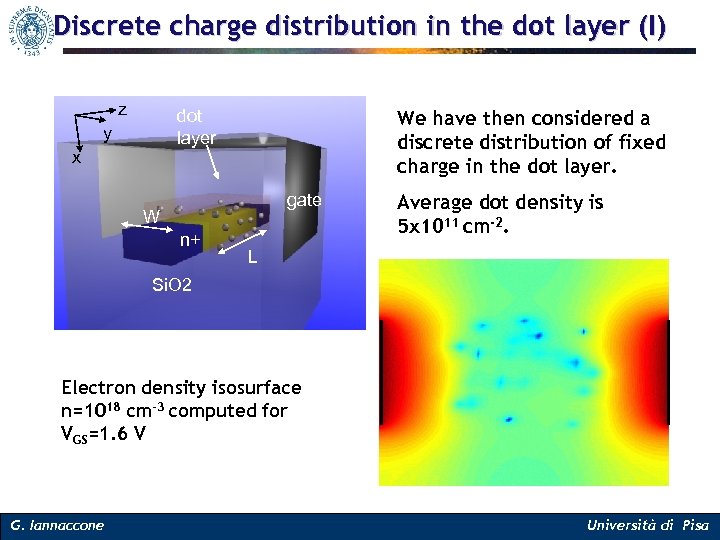
Discrete charge distribution in the dot layer (I) z dot layer y x We have then considered a discrete distribution of fixed charge in the dot layer. gate W n+ Average dot density is 5 x 1011 cm-2. L Si. O 2 Electron density isosurface n=1018 cm-3 computed for VGS=1. 6 V G. Iannaccone Università di Pisa
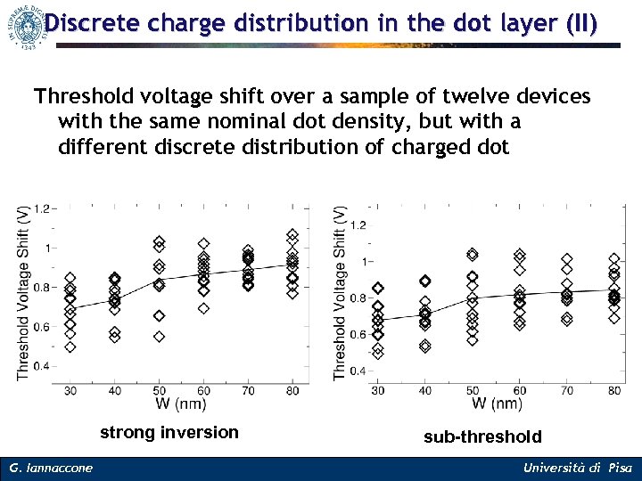
Discrete charge distribution in the dot layer (II) Threshold voltage shift over a sample of twelve devices with the same nominal dot density, but with a different discrete distribution of charged dot strong inversion G. Iannaccone sub-threshold Università di Pisa
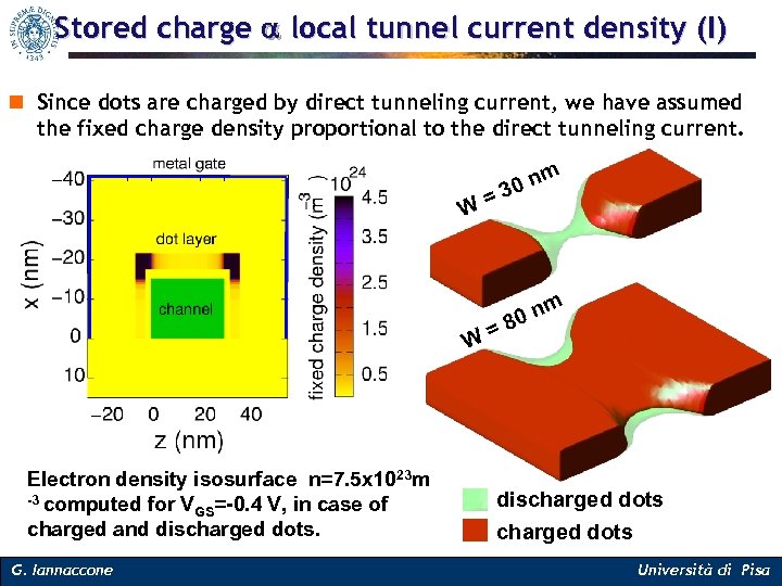
Stored charge local tunnel current density (I) n Since dots are charged by direct tunneling current, we have assumed the fixed charge density proportional to the direct tunneling current. m W= W Electron density isosurface n=7. 5 x 10²³ m -3 computed for V =-0. 4 V, in case of GS charged and discharged dots. G. Iannaccone n 30 nm 0 =8 discharged dots Università di Pisa
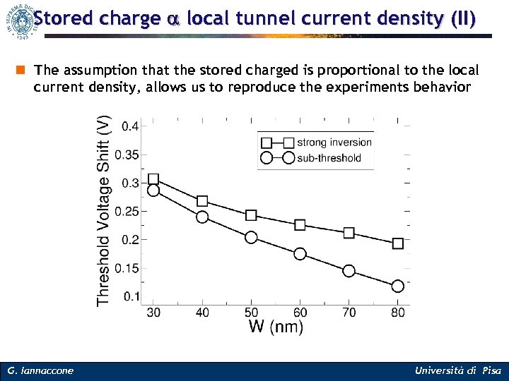
Stored charge local tunnel current density (II) n The assumption that the stored charged is proportional to the local current density, allows us to reproduce the experiments behavior G. Iannaccone Università di Pisa
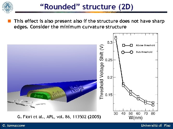
“Rounded” structure (2 D) n This effect is also present also if the structure does not have sharp edges. Consider the minimum curvature structure Above threshold Sub-threshold G. Fiori et al. , APL, vol. 86, 113502 (2005) G. Iannaccone Università di Pisa
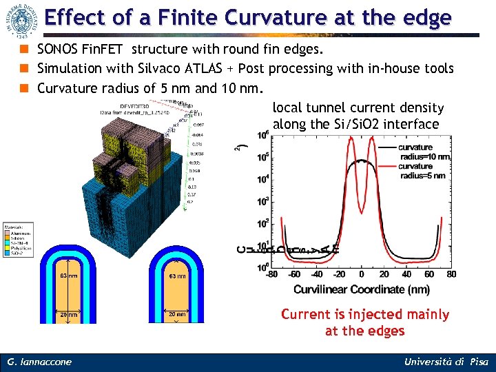
Effect of a Finite Curvature at the edge n SONOS Fin. FET structure with round fin edges. n Simulation with Silvaco ATLAS + Post processing with in-house tools n Curvature radius of 5 nm and 10 nm. local tunnel current density along the Si/Si. O 2 interface Current is injected mainly at the edges G. Iannaccone Università di Pisa
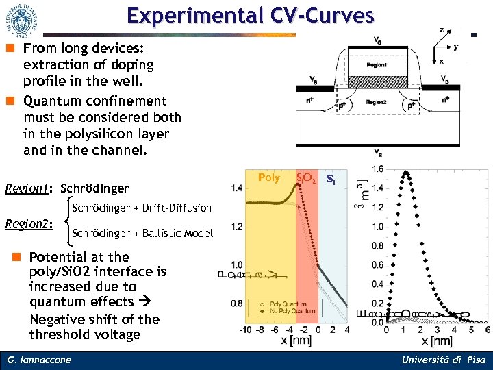
Experimental CV-Curves n From long devices: extraction of doping profile in the well. n Quantum confinement must be considered both in the polysilicon layer and in the channel. Region 1: Schrödinger Poly Si O 2 Si Schrödinger + Drift-Diffusion Region 2: Schrödinger + Ballistic Model n Potential at the poly/Si. O 2 interface is increased due to quantum effects Negative shift of the threshold voltage G. Iannaccone Università di Pisa
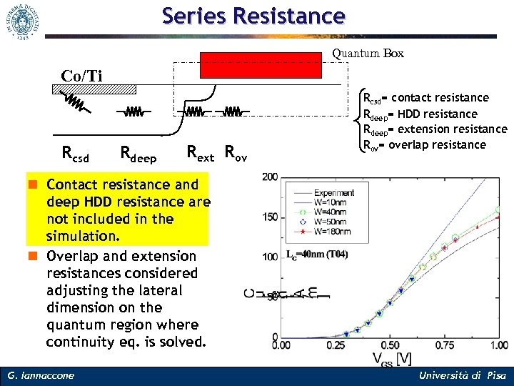
Series Resistance Quantum Box Co/Ti Rcsd Rdeep Rext Rov Rcsd= contact resistance Rdeep= HDD resistance Rdeep= extension resistance Rov= overlap resistance n Contact resistance and deep HDD resistance are not included in the simulation. n Overlap and extension resistances considered adjusting the lateral dimension on the quantum region where continuity eq. is solved. G. Iannaccone Università di Pisa
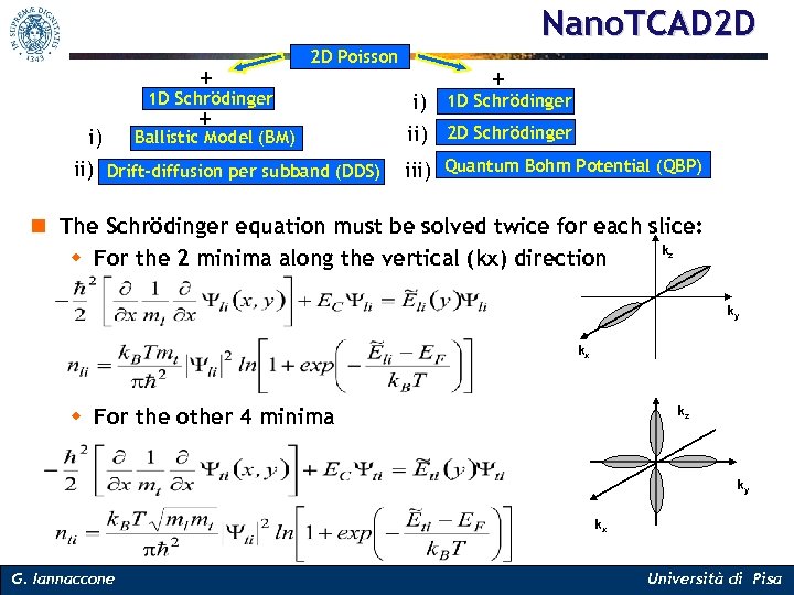
Nano. TCAD 2 D + 2 D Poisson 1 D Schrödinger + i) Ballistic Model (BM) ii) Drift-diffusion per subband (DDS) + i) ii) 1 D Schrödinger iii) Quantum Bohm Potential (QBP) 2 D Schrödinger n The Schrödinger equation must be solved twice for each slice: k w For the 2 minima along the vertical (kx) direction z ky kx w For the other 4 minima kz ky kx G. Iannaccone Università di Pisa
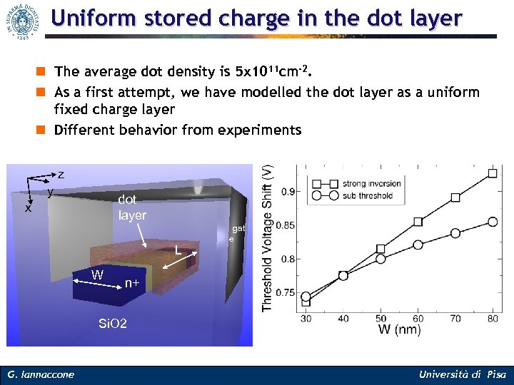
Uniform stored charge in the dot layer n The average dot density is 5 x 1011 cm-2. n As a first attempt, we have modelled the dot layer as a uniform fixed charge layer n Different behavior from experiments z y dot layer x L W gat e n+ Si. O 2 G. Iannaccone Università di Pisa
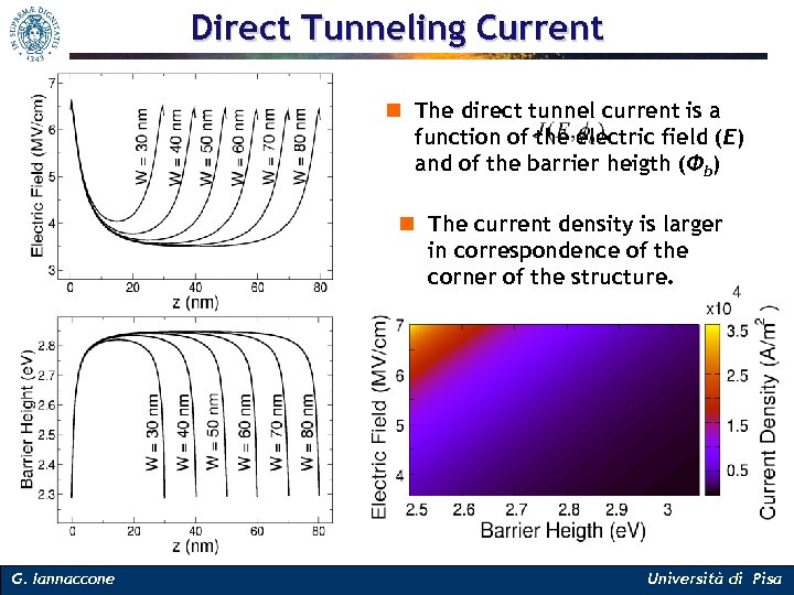
Direct Tunneling Current n The direct tunnel current is a function of the electric field (E) and of the barrier heigth (Φb) n The current density is larger in correspondence of the corner of the structure. G. Iannaccone Università di Pisa
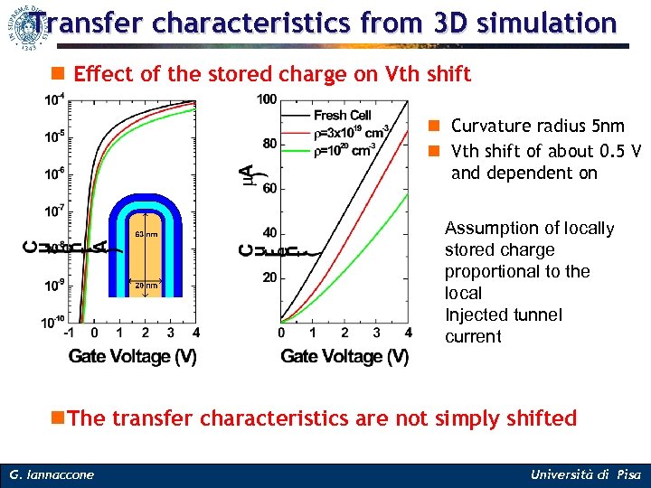
Transfer characteristics from 3 D simulation n Effect of the stored charge on Vth shift n Curvature radius 5 nm n Vth shift of about 0. 5 V and dependent on Assumption of locally stored charge proportional to the local Injected tunnel current n. The transfer characteristics are not simply shifted G. Iannaccone Università di Pisa
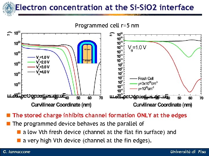
Electron concentration at the Si-Si. O 2 interface Programmed cell r=5 nm n The stored charge inhibits channel formation ONLY at the edges n The programmed device behaves as the parallel of n a low Vth fresh device (channel at the flat fin surface) and n a very high Vth device (channel at the fin edges). G. Iannaccone Università di Pisa
58eaa733b9b799c7273b324887bb5caa.ppt