86e5db27df5ce0caa4e9adaa83d03510.ppt
- Количество слайдов: 99
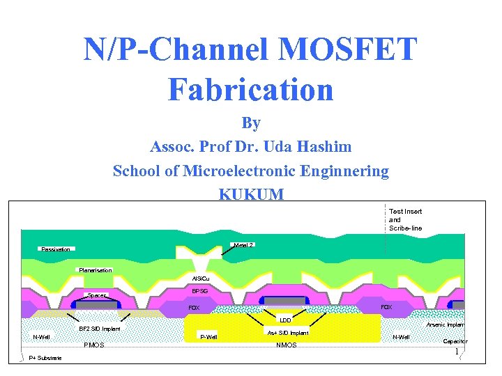
N/P-Channel MOSFET Fabrication By Assoc. Prof Dr. Uda Hashim School of Microelectronic Enginnering KUKUM Test Insert and Scribe-line Metal 2 Passivation Planarisation Al. Si. Cu Spacer BPSG FOX LDD BF 2 S/D Implant N-Well PMOS P+ Substrate As+ S/D Implant NMOS Arsenic Implant N-Well Capacitor 1
Overview • • • Integrated Circuit Manufacturing Process Mask Design and Layout Main Fabrication Process Transistor Fabrication Step by Step Electrical Characterization and Testing Fabrication Documents (Runcard) Preparation 2
The making of transistor • • • Circuit design Mask/layout design Mask making and artwork Fabrication process Device testing – for parametric and functional test • Packaging and Reliability Test 3
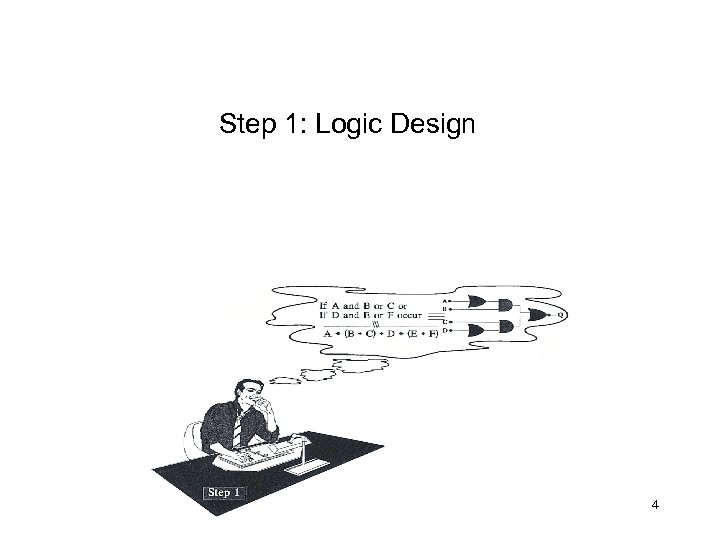
Step 1: Logic Design 4
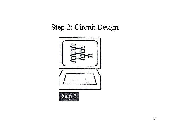
Step 2: Circuit Design 5
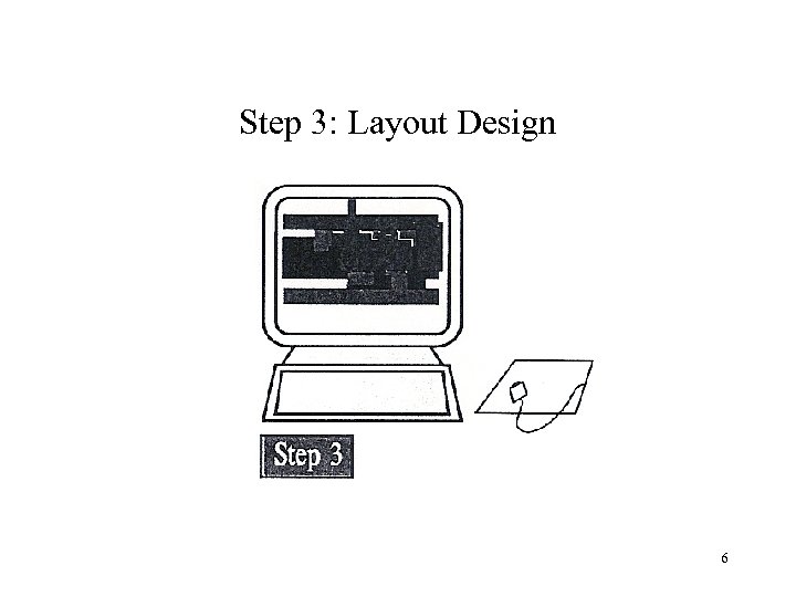
Step 3: Layout Design 6
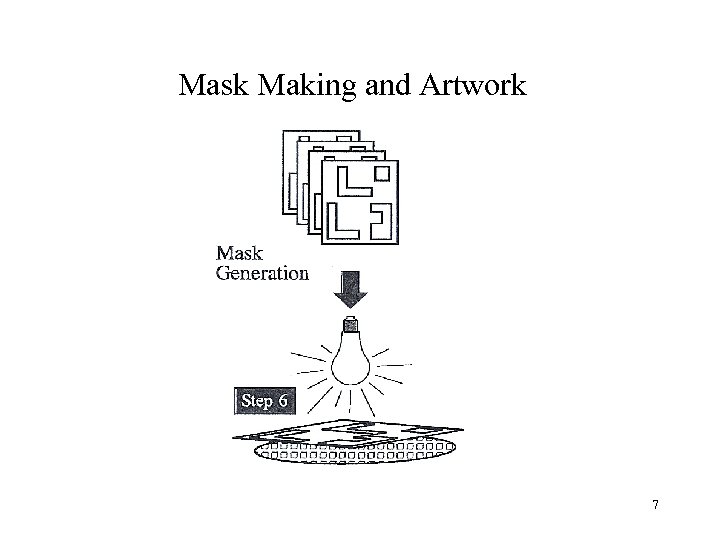
Mask Making and Artwork 7
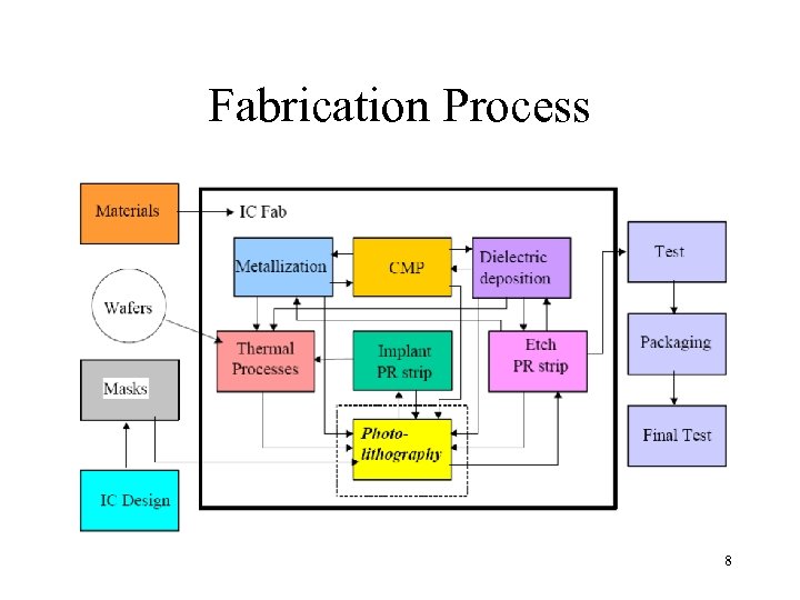
Fabrication Process 8
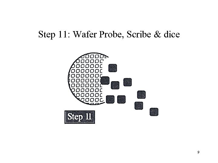
Step 11: Wafer Probe, Scribe & dice 9
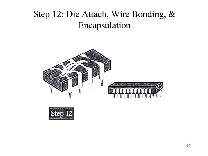
Step 12: Die Attach, Wire Bonding, & Encapsulation 10
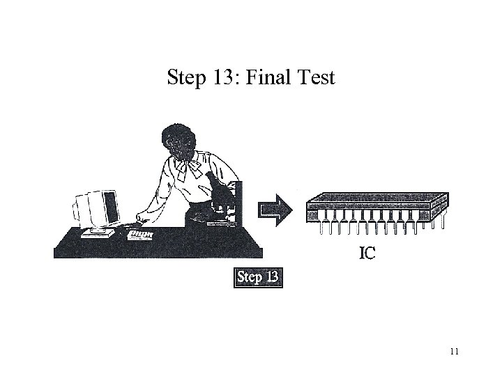
Step 13: Final Test 11

Mask Design 12
MOSFET Masking Step • • Mask 1: Source Drain Mask 2: Gate Mask 3: Contact mask Mask 4: Metallization Mask 13
Introduction • Mask design is very important before fabrication process can be done. • Design rules must be followed to prevent defect in the process. • In this design, gate length is varied from 30 um, 50 um, 100 um, 150 um, 200 um and 300 um. • Different gate length will have different gate mask and different distance from source to drain. • The smaller the gate size, the better the transistor in speed. 14
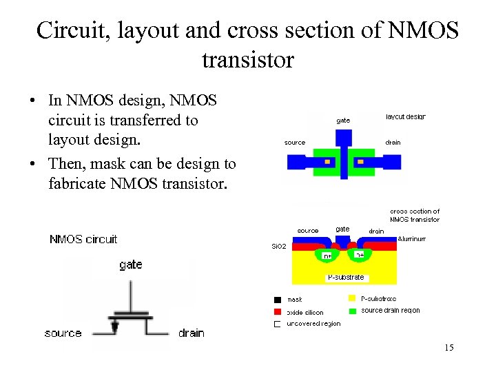
Circuit, layout and cross section of NMOS transistor • In NMOS design, NMOS circuit is transferred to layout design. • Then, mask can be design to fabricate NMOS transistor. 15
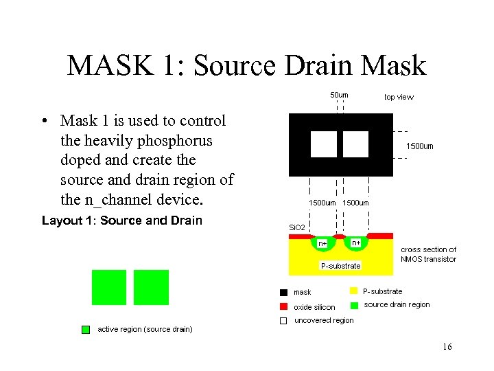
MASK 1: Source Drain Mask • Mask 1 is used to control the heavily phosphorus doped and create the source and drain region of the n_channel device. Layout 1: Source and Drain 16
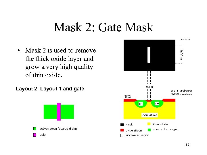
Mask 2: Gate Mask • Mask 2 is used to remove thick oxide layer and grow a very high quality of thin oxide. Layout 2: Layout 1 and gate 17
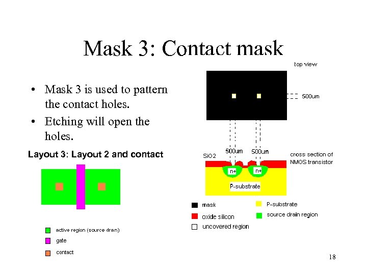
Mask 3: Contact mask • Mask 3 is used to pattern the contact holes. • Etching will open the holes. Layout 3: Layout 2 and contact 18
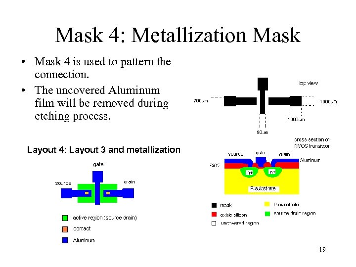
Mask 4: Metallization Mask • Mask 4 is used to pattern the connection. • The uncovered Aluminum film will be removed during etching process. Layout 4: Layout 3 and metallization 19

Mask Design (Step by Step) 20
Photo Mask Preparation • Apply Auto. CAD to design the masks • Transfer the pattern to high resolution printer 21
Mask Design Step • Step 1: Set frame and wafer size dimension • Step 2: Design alignment mark • Step 3: Design source and drain mask (Mask 1) block and duplicate to the whole wafer. • Step 4: Design gate mask (Mask 2) block and duplicate to the whole wafer. Then, inverse the alignment mark to change the polarity. 22
• Step 5: Design contact mask (Mask 3) block and duplicate to the whole wafer. • Step 6: Design Metallization mask (Mask 4) block and duplicate to the whole mask. • Step 7: Print on transparency film using high resolution printer. 23
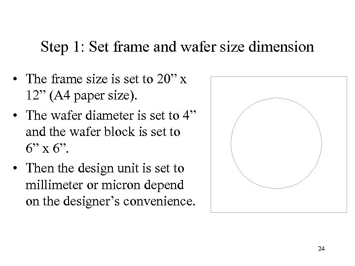
Step 1: Set frame and wafer size dimension • The frame size is set to 20” x 12” (A 4 paper size). • The wafer diameter is set to 4” and the wafer block is set to 6” x 6”. • Then the design unit is set to millimeter or micron depend on the designer’s convenience. 24
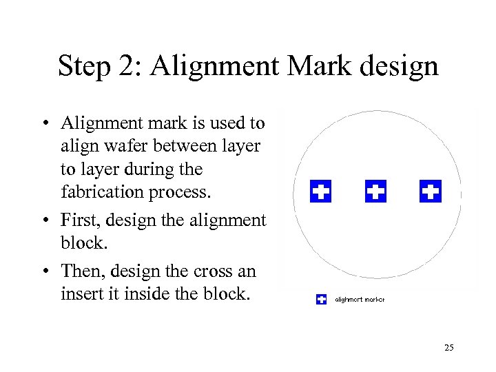
Step 2: Alignment Mark design • Alignment mark is used to align wafer between layer to layer during the fabrication process. • First, design the alignment block. • Then, design the cross an insert it inside the block. 25
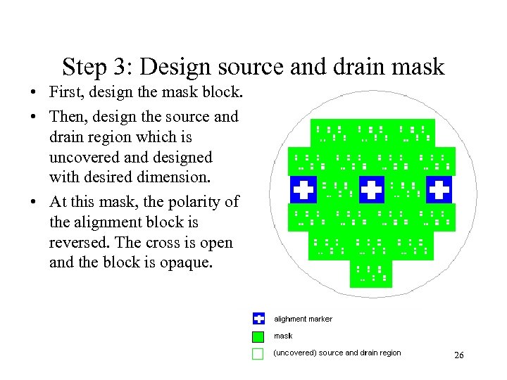
Step 3: Design source and drain mask • First, design the mask block. • Then, design the source and drain region which is uncovered and designed with desired dimension. • At this mask, the polarity of the alignment block is reversed. The cross is open and the block is opaque. 26
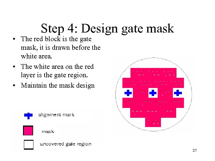
Step 4: Design gate mask • The red block is the gate mask, it is drawn before the white area. • The white area on the red layer is the gate region. • Maintain the mask design 27
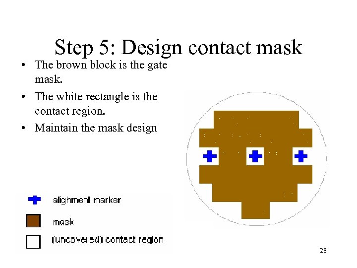
Step 5: Design contact mask • The brown block is the gate mask. • The white rectangle is the contact region. • Maintain the mask design 28
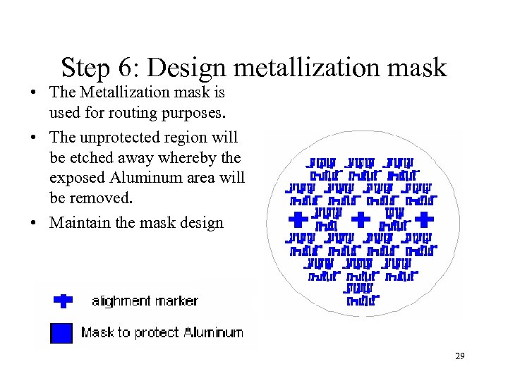
Step 6: Design metallization mask • The Metallization mask is used for routing purposes. • The unprotected region will be etched away whereby the exposed Aluminum area will be removed. • Maintain the mask design 29

Actual Transparency Masks 30

Q & A 31
EQUIPMENTS AND CONSUMABLES 32
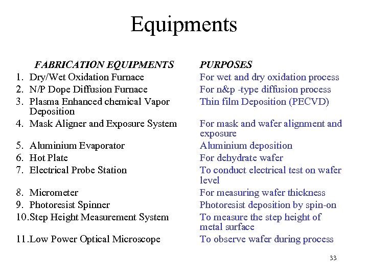
Equipments 1. 2. 3. 4. FABRICATION EQUIPMENTS Dry/Wet Oxidation Furnace N/P Dope Diffusion Furnace Plasma Enhanced chemical Vapor Deposition Mask Aligner and Exposure System 5. Aluminium Evaporator 6. Hot Plate 7. Electrical Probe Station 8. Micrometer 9. Photoresist Spinner 10. Step Height Measurement System 11. Low Power Optical Microscope PURPOSES For wet and dry oxidation process For n&p -type diffusion process Thin film Deposition (PECVD) For mask and wafer alignment and exposure Aluminium deposition For dehydrate wafer To conduct electrical test on wafer level For measuring wafer thickness Photoresist deposition by spin-on To measure the step height of metal surface To observe wafer during process 33
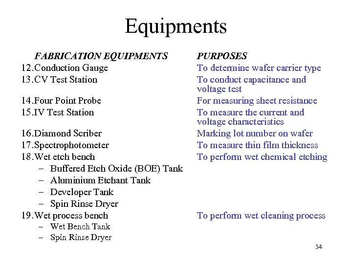
Equipments FABRICATION EQUIPMENTS 12. Conduction Gauge 13. CV Test Station 14. Four Point Probe 15. IV Test Station 16. Diamond Scriber 17. Spectrophotometer 18. Wet etch bench – Buffered Etch Oxide (BOE) Tank – Aluminium Etchant Tank – Developer Tank – Spin Rinse Dryer 19. Wet process bench PURPOSES To determine wafer carrier type To conduct capacitance and voltage test For measuring sheet resistance To measure the current and voltage characteristics Marking lot number on wafer To measure thin film thickness To perform wet chemical etching To perform wet cleaning process – Wet Bench Tank – Spin Rinse Dryer 34
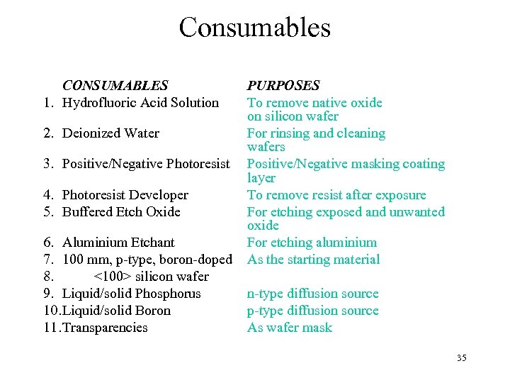
Consumables CONSUMABLES 1. Hydrofluoric Acid Solution PURPOSES To remove native oxide on silicon wafer 2. Deionized Water For rinsing and cleaning wafers 3. Positive/Negative Photoresist Positive/Negative masking coating layer 4. Photoresist Developer To remove resist after exposure 5. Buffered Etch Oxide For etching exposed and unwanted oxide 6. Aluminium Etchant For etching aluminium 7. 100 mm, p-type, boron-doped As the starting material 8. <100> silicon wafer 9. Liquid/solid Phosphorus n-type diffusion source 10. Liquid/solid Boron p-type diffusion source 11. Transparencies As wafer mask 35
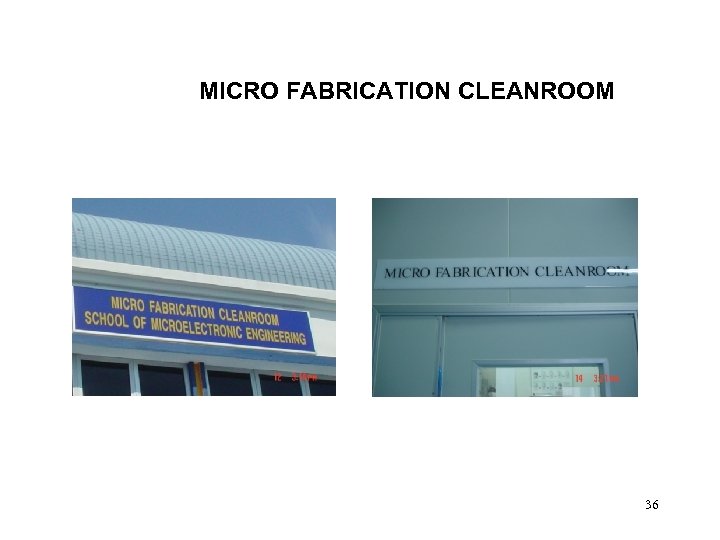
MICRO FABRICATION CLEANROOM 36
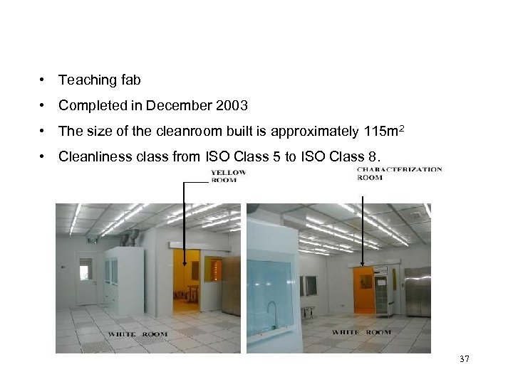
• Teaching fab • Completed in December 2003 • The size of the cleanroom built is approximately 115 m 2 • Cleanliness class from ISO Class 5 to ISO Class 8. 37
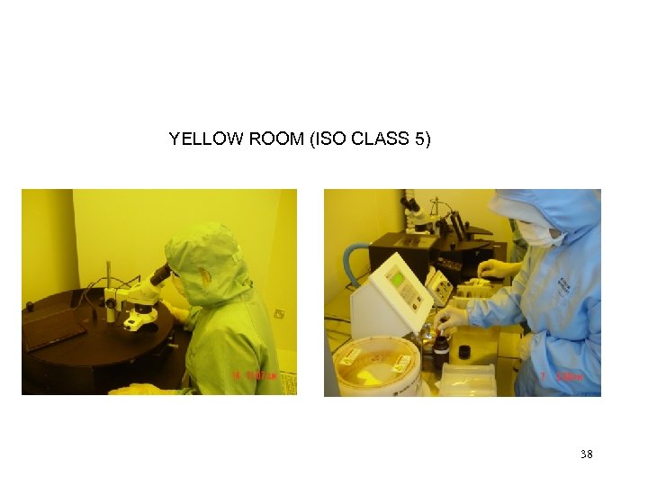
YELLOW ROOM (ISO CLASS 5) 38
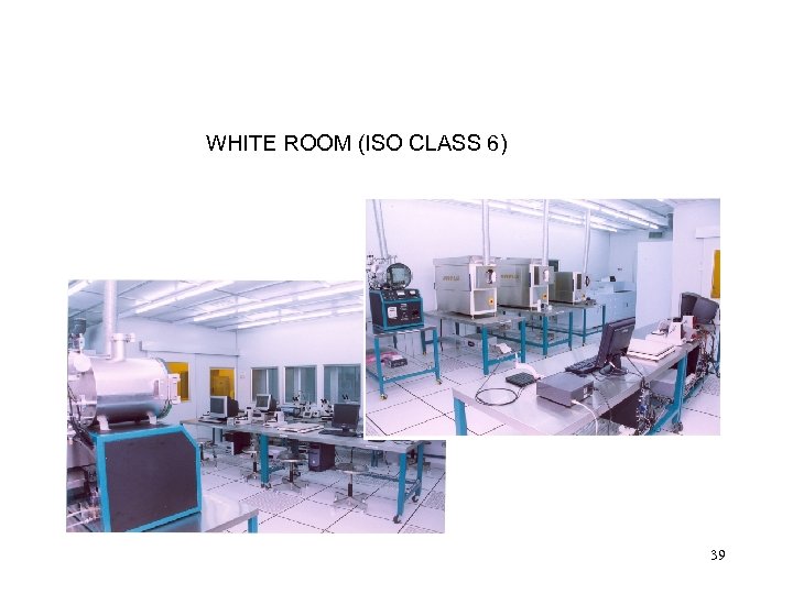
WHITE ROOM (ISO CLASS 6) 39
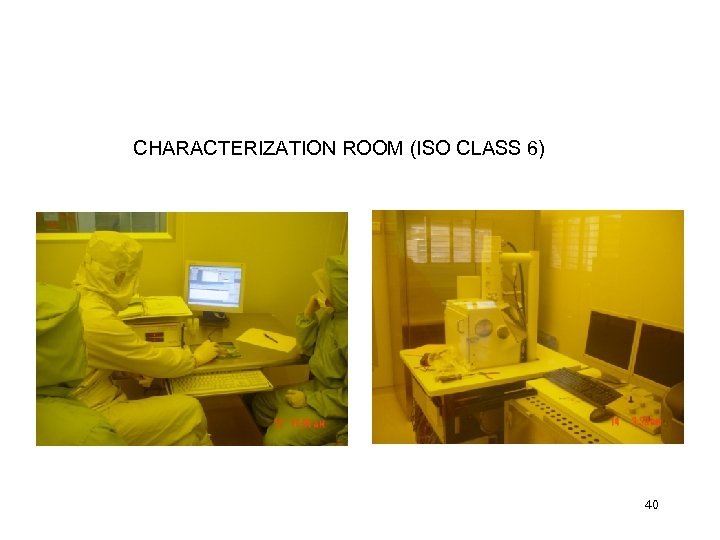
CHARACTERIZATION ROOM (ISO CLASS 6) 40
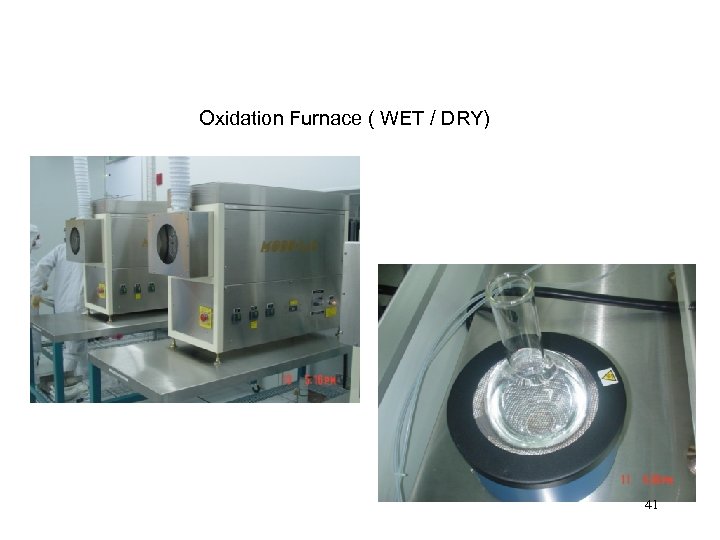
Oxidation Furnace ( WET / DRY) 41
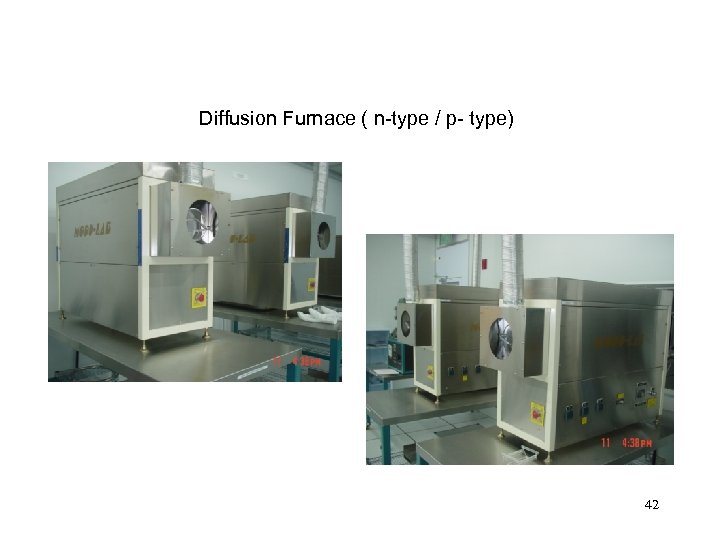
Diffusion Furnace ( n-type / p- type) 42
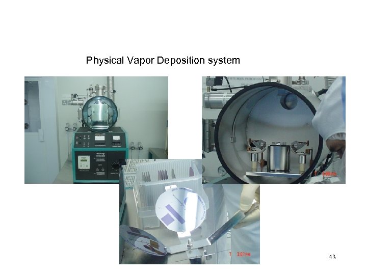
Physical Vapor Deposition system 43
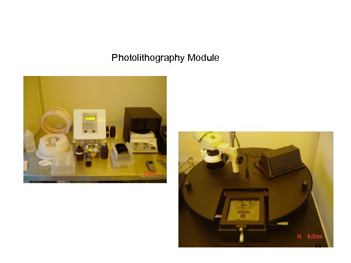
Photolithography Module 44
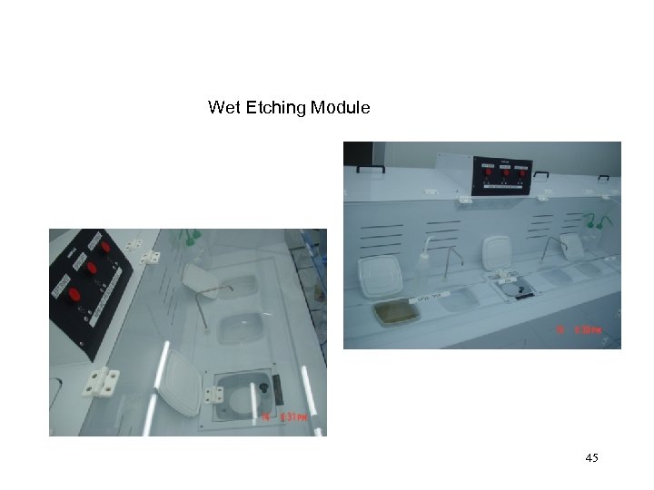
Wet Etching Module 45
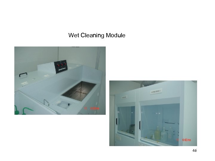
Wet Cleaning Module 46
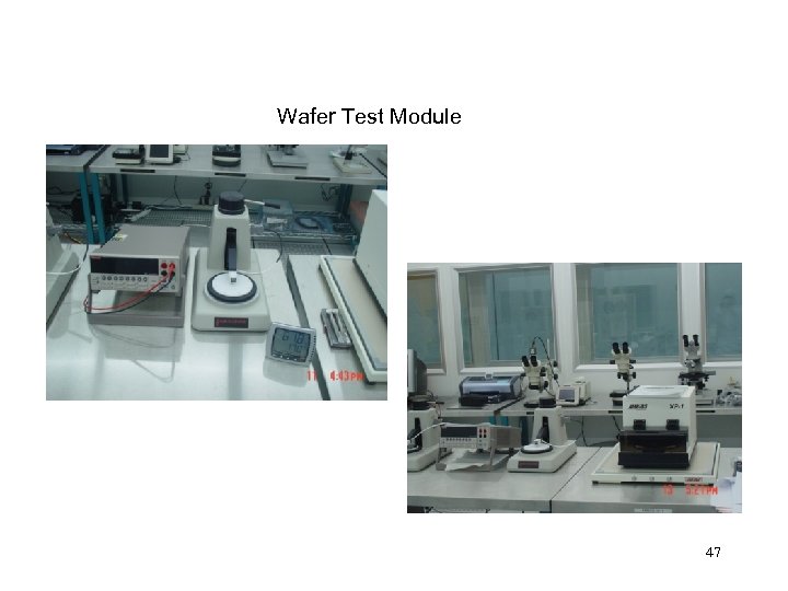
Wafer Test Module 47
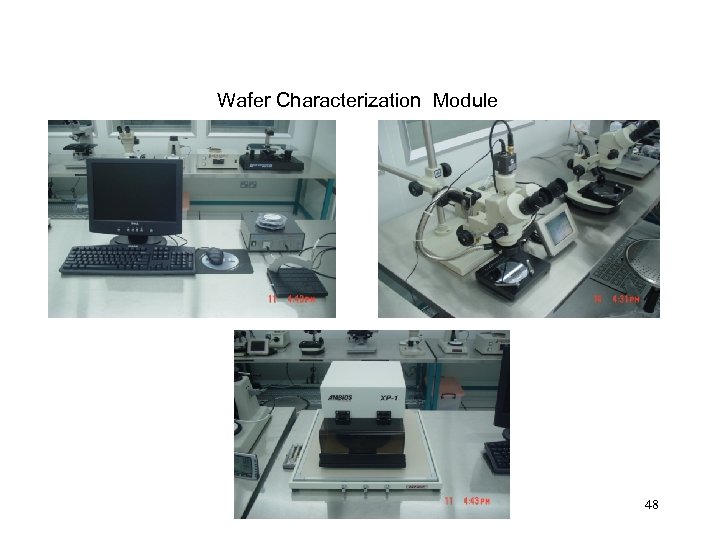
Wafer Characterization Module 48
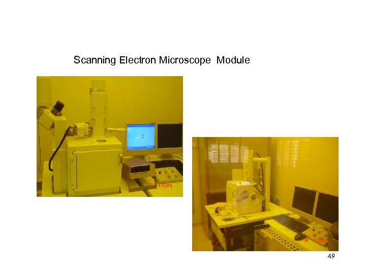
Scanning Electron Microscope Module 49
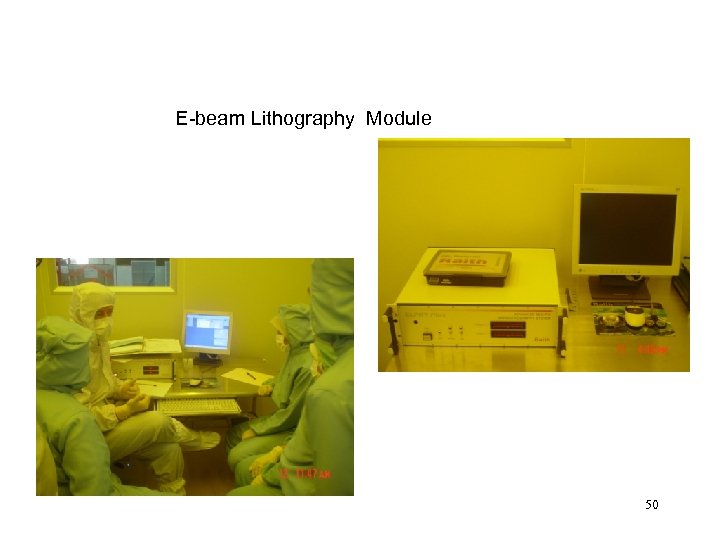
E-beam Lithography Module 50
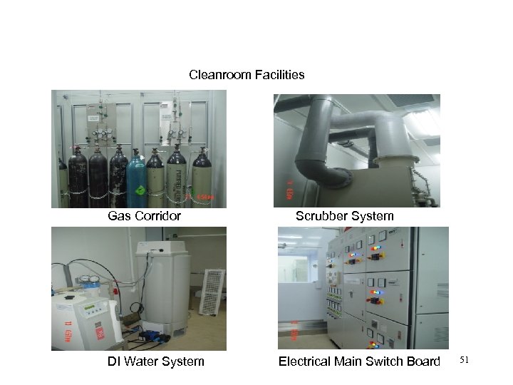
Cleanroom Facilities Gas Corridor DI Water System Scrubber System Electrical Main Switch Board 51
Main Fabrication Process 52
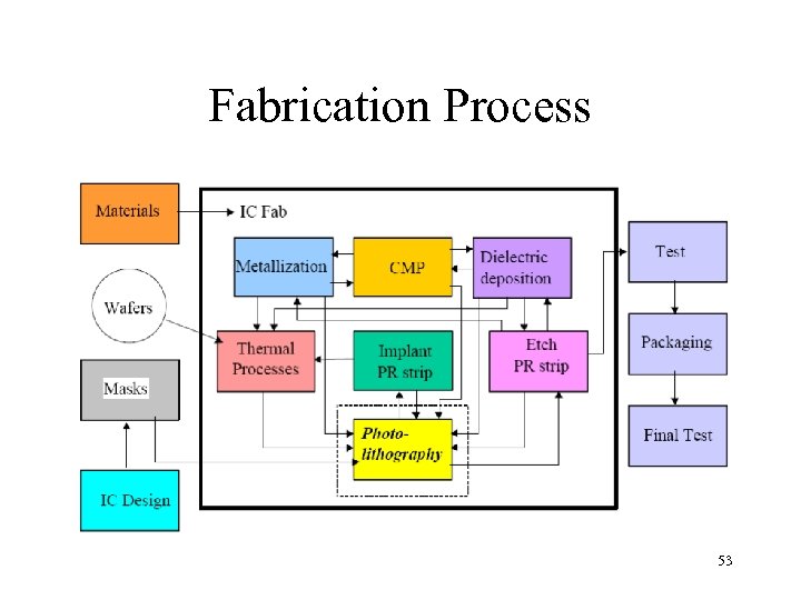
Fabrication Process 53
Pre-Oxidation Clean Cycle • The SC-1 (RCA) clean is used to remove particles and organic materials by oxidizing the particle • NH 4 OH : H 2 O 2 : H 2 O with the ratio 1 : 4 : 50 • Temperature ~75℃ with 10 minutes duration and rinse by DI water ~3 minutes 54
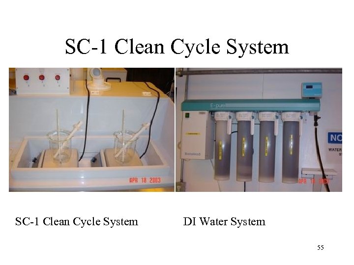
SC-1 Clean Cycle System DI Water System 55
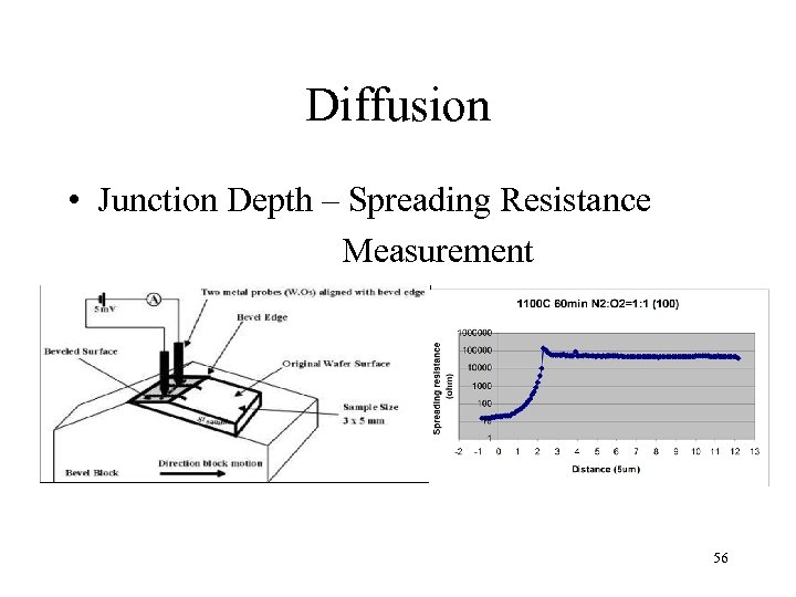
Diffusion • Junction Depth – Spreading Resistance Measurement 56
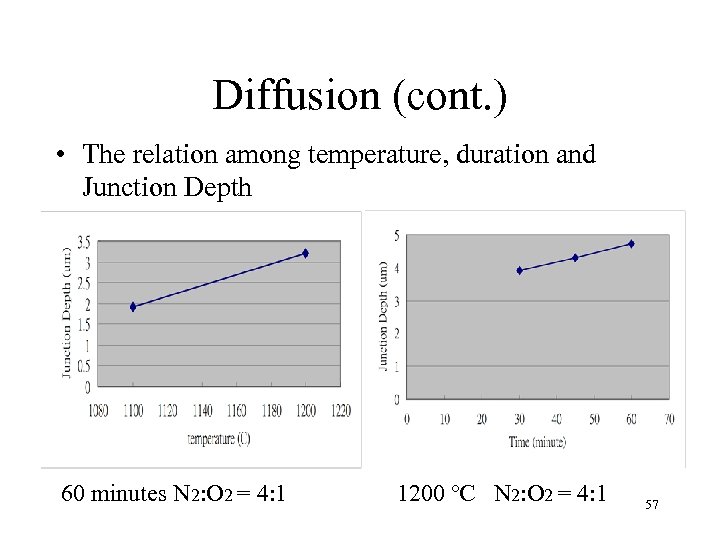
Diffusion (cont. ) • The relation among temperature, duration and Junction Depth 60 minutes N 2: O 2 = 4: 1 1200 ℃ N 2: O 2 = 4: 1 57
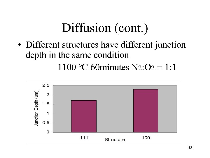
Diffusion (cont. ) • Different structures have different junction depth in the same condition 1100 ℃ 60 minutes N 2: O 2 = 1: 1 58
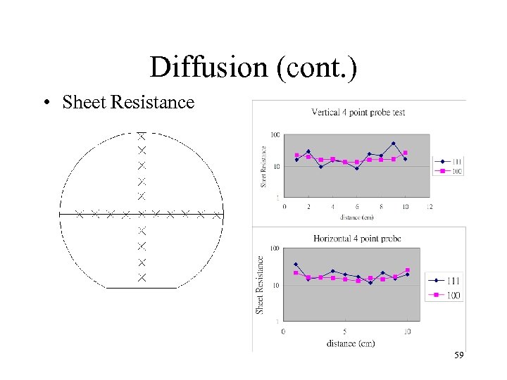
Diffusion (cont. ) • Sheet Resistance 59
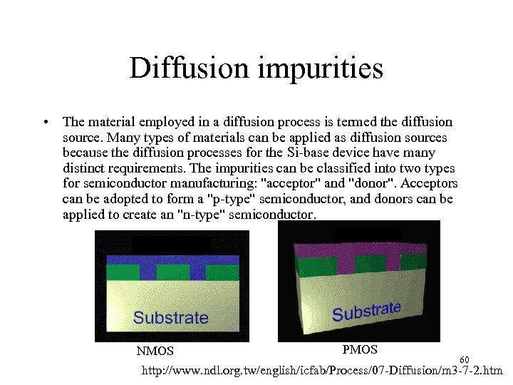
Diffusion impurities • The material employed in a diffusion process is termed the diffusion source. Many types of materials can be applied as diffusion sources because the diffusion processes for the Si-base device have many distinct requirements. The impurities can be classified into two types for semiconductor manufacturing: "acceptor" and "donor". Acceptors can be adopted to form a "p-type" semiconductor, and donors can be applied to create an "n-type" semiconductor. PMOS NMOS 60 http: //www. ndl. org. tw/english/icfab/Process/07 -Diffusion/m 3 -7 -2. htm
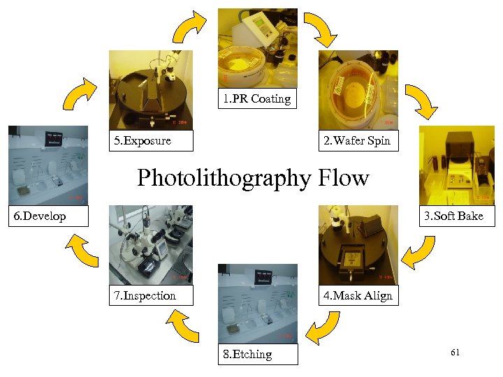
1. PR Coating 2. Wafer Spin 5. Exposure Photolithography Flow 6. Develop 3. Soft Bake 4. Mask Align 7. Inspection 8. Etching 61
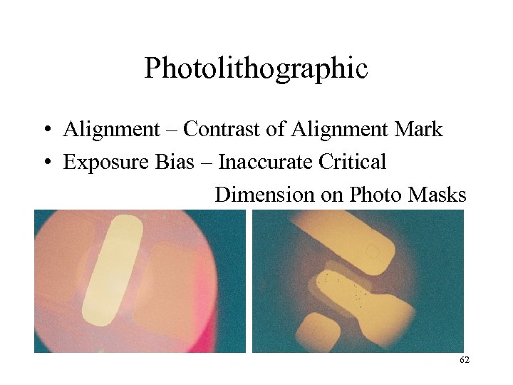
Photolithographic • Alignment – Contrast of Alignment Mark • Exposure Bias – Inaccurate Critical Dimension on Photo Masks 62
Transistor Fabrication (Step by Step Process) 63
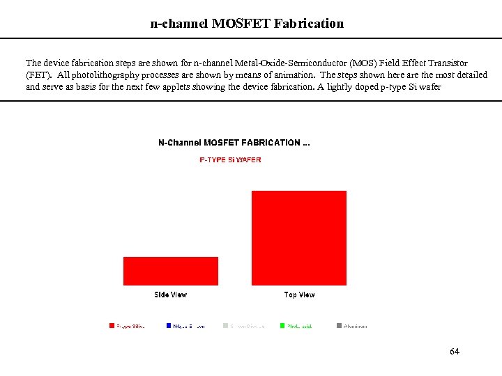
n-channel MOSFET Fabrication The device fabrication steps are shown for n-channel Metal-Oxide-Semiconductor (MOS) Field Effect Transistor (FET). All photolithography processes are shown by means of animation. The steps shown here are the most detailed and serve as basis for the next few applets showing the device fabrication. A lightly doped p-type Si wafer 64
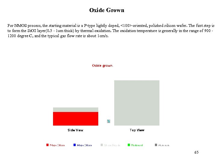
Oxide Grown For NMOS process, the starting material is a P-type lightly doped, <100>-oriented, polished silicon wafer. The first step is to form the Si. O 2 layer(0. 5 - 1 um thick) by thermal oxidation. The oxidation temperature is generally in the range of 900 - 1200 degree C, and the typical gas flow rate is about 1 cm/s. 65
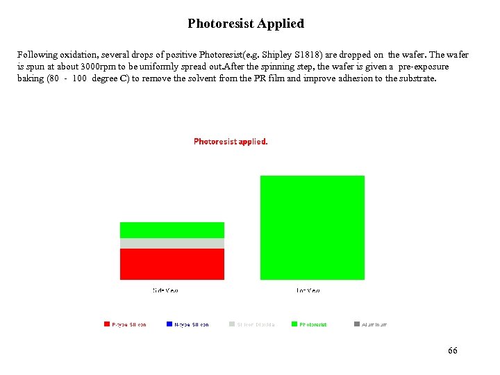
Photoresist Applied Following oxidation, several drops of positive Photoresist(e. g. Shipley S 1818) are dropped on the wafer. The wafer is spun at about 3000 rpm to be uniformly spread out. After the spinning step, the wafer is given a pre-exposure baking (80 - 100 degree C) to remove the solvent from the PR film and improve adhesion to the substrate. 66
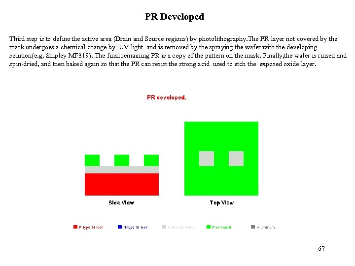
PR Developed Third step is to define the active area (Drain and Source regions) by photolithography. The PR layer not covered by the mask undergoes a chemical change by UV light and is removed by the spraying the wafer with the developing solution(e. g. Shipley MF 319). The final remaining PR is a copy of the pattern on the mask. Finally, the wafer is rinsed and spin-dried, and then baked again so that the PR can resist the strong acid used to etch the exposed oxide layer. 67
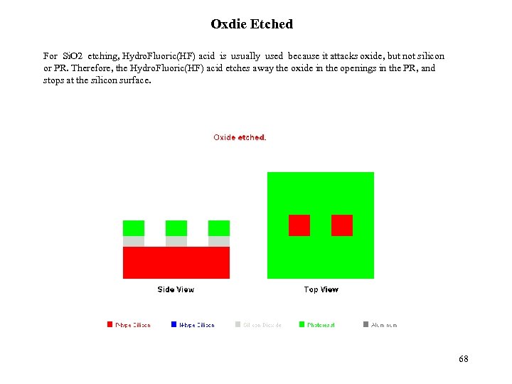
Oxdie Etched For Si. O 2 etching, Hydro. Fluoric(HF) acid is usually used because it attacks oxide, but not silicon or PR. Therefore, the Hydro. Fluoric(HF) acid etches away the oxide in the openings in the PR, and stops at the silicon surface. 68
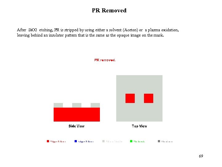
PR Removed After Si. O 2 etching, PR is stripped by using either a solvent (Aceton) or a plasma oxidation, leaving behind an insulator pattern that is the same as the opaque image on the mask. 69
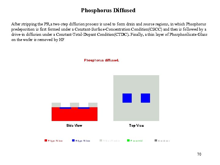
Phosphorus Diffused After stripping the PR, a two-step diffusion process is used to form drain and source regions, in which Phosphorus predeposition is first formed under a Constant-Surface-Concentration Condition(CSCC) and then is followed by a drive-in diffusion under a Constant-Total-Dopant Condition(CTDC). Finally, a thin layer of Phosphosilicate Glass on the wafer is removed by HF 70
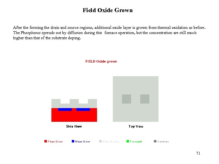
Field Oxide Grown After the forming the drain and source regions, additional oxide layer is grown from thermal oxidation as before. The Phosphorus spreads out by diffusion during this furnace operation, but the concentration are still much higher than that of the substrate doping. 71
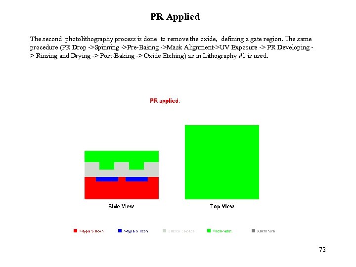
PR Applied The second photolithography process is done to remove the oxide, defining a gate region. The same procedure (PR Drop ->Spinning ->Pre-Baking ->Mask Alignment->UV Exposure -> PR Developing > Rinsing and Drying -> Post-Baking -> Oxide Etching) as in Lithography #1 is used. 72

PR Developed The second photolithography process is done to remove the oxide, defining a gate region. The same procedure (PR Drop ->Spinning ->Pre-Baking ->Mask Alignment->UV Exposure -> PR Developing > Rinsing and Drying -> Post-Baking -> Oxide Etching) as in Lithography #1 is used. 73
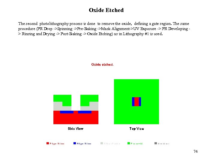
Oxide Etched The second photolithography process is done to remove the oxide, defining a gate region. The same procedure (PR Drop ->Spinning ->Pre-Baking ->Mask Alignment->UV Exposure -> PR Developing > Rinsing and Drying -> Post-Baking -> Oxide Etching) as in Lithography #1 is used. 74
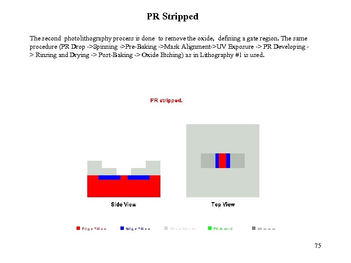
PR Stripped The second photolithography process is done to remove the oxide, defining a gate region. The same procedure (PR Drop ->Spinning ->Pre-Baking ->Mask Alignment->UV Exposure -> PR Developing > Rinsing and Drying -> Post-Baking -> Oxide Etching) as in Lithography #1 is used. 75
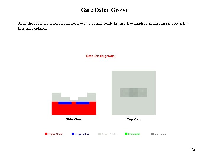
Gate Oxide Grown After the second photolithography, a very thin gate oxide layer(a few hundred angstroms) is grown by thermal oxidation. 76
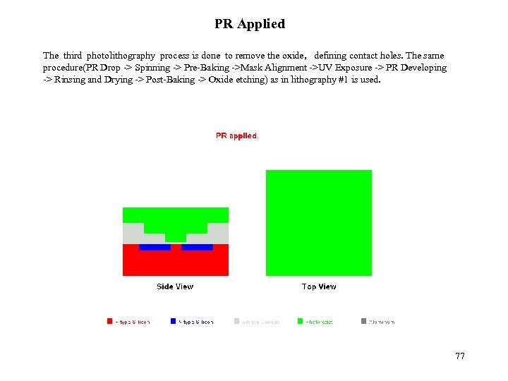
PR Applied The third photolithography process is done to remove the oxide, defining contact holes. The same procedure(PR Drop -> Spinning -> Pre-Baking ->Mask Alignment ->UV Exposure -> PR Developing -> Rinsing and Drying -> Post-Baking -> Oxide etching) as in lithography #1 is used. 77
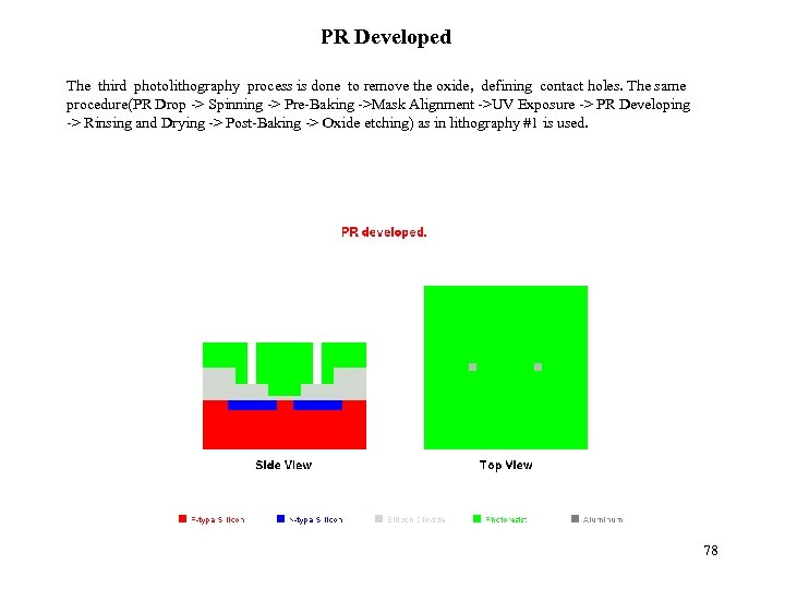
PR Developed The third photolithography process is done to remove the oxide, defining contact holes. The same procedure(PR Drop -> Spinning -> Pre-Baking ->Mask Alignment ->UV Exposure -> PR Developing -> Rinsing and Drying -> Post-Baking -> Oxide etching) as in lithography #1 is used. 78

Oxide Etched The third photolithography process is done to remove the oxide, defining contact holes. The same procedure(PR Drop -> Spinning -> Pre-Baking ->Mask Alignment ->UV Exposure -> PR Developing -> Rinsing and Drying -> Post-Baking -> Oxide etching) as in lithography #1 is used. 79
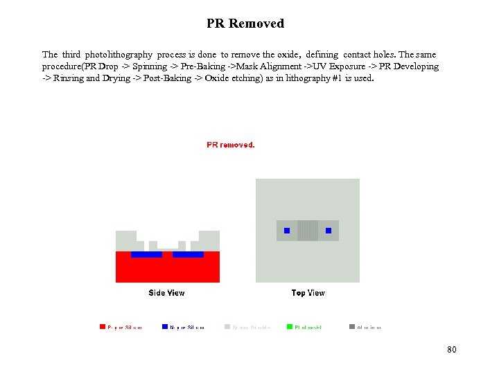
PR Removed The third photolithography process is done to remove the oxide, defining contact holes. The same procedure(PR Drop -> Spinning -> Pre-Baking ->Mask Alignment ->UV Exposure -> PR Developing -> Rinsing and Drying -> Post-Baking -> Oxide etching) as in lithography #1 is used. 80
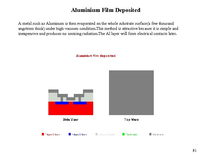
Aluminium Film Deposited A metal such as Aluminum is then evaporated on the whole substrate surface(a few thousand angstrom thick) under high-vacuum condition. This method is attractive because it is simple and inexpensive and produces no ionizing radiation. The Al layer will form electrical contacts later. 81
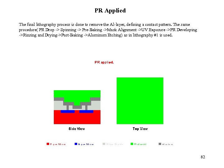
PR Applied The final lithography process is done to remove the Al-layer, defining a contact pattern. The same procedure( PR Drop -> Spinning -> Pre-Baking ->Mask Alignment ->UV Exposure ->PR Developing ->Rinsing and Drying->Post-Baking ->Aluminum Etching) as in lithography #1 is used. 82
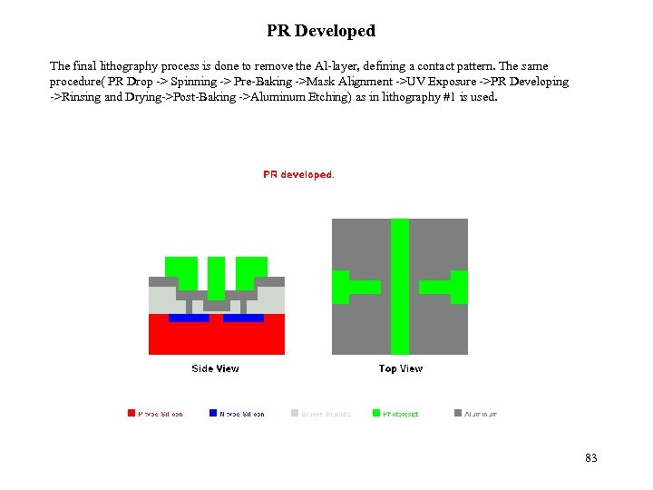
PR Developed The final lithography process is done to remove the Al-layer, defining a contact pattern. The same procedure( PR Drop -> Spinning -> Pre-Baking ->Mask Alignment ->UV Exposure ->PR Developing ->Rinsing and Drying->Post-Baking ->Aluminum Etching) as in lithography #1 is used. 83
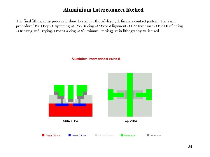
Aluminium Interconnect Etched The final lithography process is done to remove the Al-layer, defining a contact pattern. The same procedure( PR Drop -> Spinning -> Pre-Baking ->Mask Alignment ->UV Exposure ->PR Developing ->Rinsing and Drying->Post-Baking ->Aluminum Etching) as in lithography #1 is used. 84
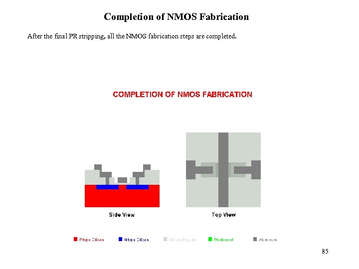
Completion of NMOS Fabrication After the final PR stripping, all the NMOS fabrication steps are completed. 85
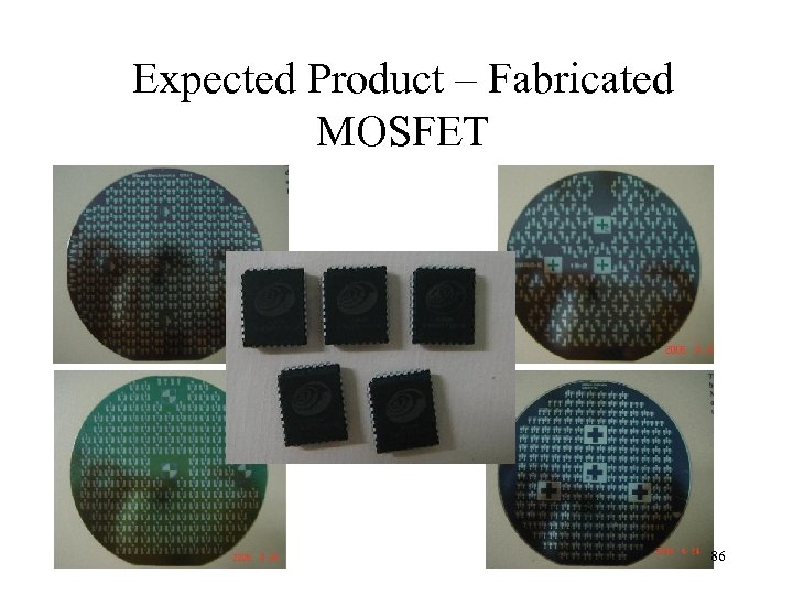
Expected Product – Fabricated MOSFET 86
Electrical Characterization and Testing 87
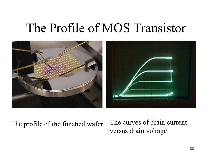
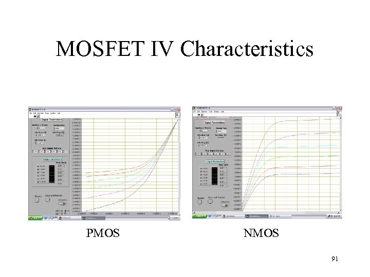
The Profile of MOS Transistor The profile of the finished wafer The curves of drain current versus drain voltage 88
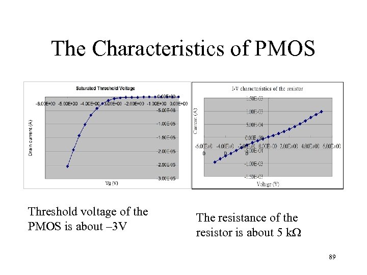
The Characteristics of PMOS Threshold voltage of the PMOS is about – 3 V The resistance of the resistor is about 5 kΩ 89
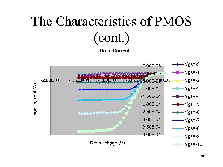
The Characteristics of PMOS (cont. ) 90
MOSFET IV Characteristics PMOS NMOS 91
Fabrication Documents (Runcard) Preparation 92
Process Flow Development Diagram 93
Runcard Checklist • • Process runcard Measurement sheet Rework sheet Equipments list Consumables list Design specification Complete Mask Design 94
Process Runcard • No. of process steps = 71 • No of process module = 11 • Shall include the following information; – – – Step number Equipment ID Wafer out Time in/out Date out Remarks 95
Measurement sheet • • • Total Number of measurement = 35 Sheet Resistance Measurement = 6 Oxide Thickness Measurement = 9 Resist Thickness Measurement = 4 CD Measurement = 7 96
Rework sheet • Only for lithography process 97
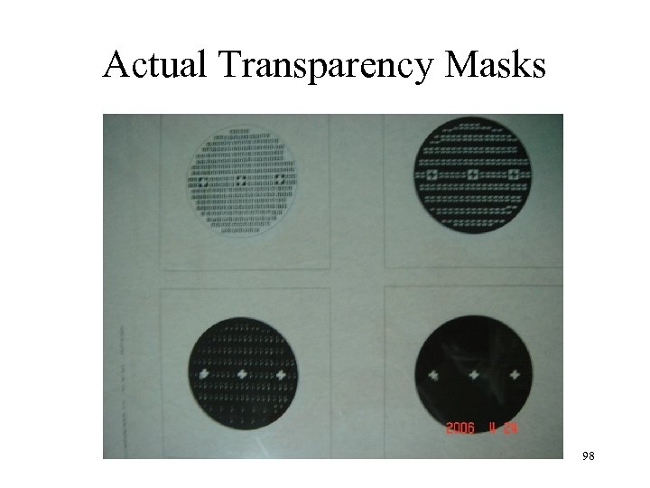
Actual Transparency Masks 98

Thanks 99
86e5db27df5ce0caa4e9adaa83d03510.ppt