ac15cc7ebff202d89491e34cd230b138.ppt
- Количество слайдов: 172
 Multithreaded Processors Dezső Sima Spring 2007 (Ver. 2. 1) Dezső Sima, 2007
 Overview • 1. Introduction • 2. Overview of multithreaded cores • 3. Thread scheduling • 4. Case examples • 4. 1. Coarse grained multithreaded cores • 4. 2. Fine grained multithreaded cores • 4. 3. SMT cores
 1. Introduction
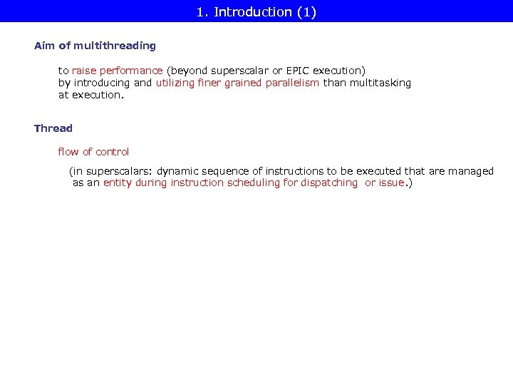 1. Introduction (1) Aim of multithreading to raise performance (beyond superscalar or EPIC execution) by introducing and utilizing finer grained parallelism than multitasking at execution. Thread flow of control (in superscalars: dynamic sequence of instructions to be executed that are managed as an entity during instruction scheduling for dispatching or issue. )
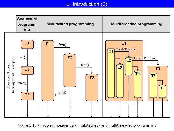 1. Introduction (2) Sequential programm ing P 1 Multitasked programming P 1 Multithreaded programming P 1 fork() Process / Thread Management Example T 1 Create. Thread() P 2 exec() T 2 fork() Create Process() T 3 P 2 P 3 P 2 T 4 T 5 exec() T 6 P 3 join() Figure 1. 1: Principle of sequential-, multitasked- and multithreaded programming
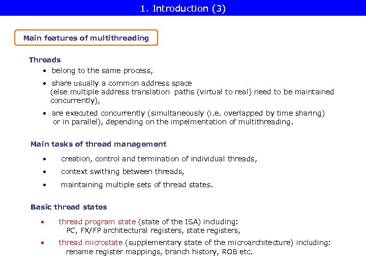 1. Introduction (3) Main features of multithreading Threads • belong to the same process, • share usually a common address space (else multiple address translation paths (virtual to real) need to be maintained concurrently), • are executed concurrently (simultaneously (i. e. overlapped by time sharing) or in parallel), depending on the impelmentation of multithreading. Main tasks of thread management • creation, control and termination of individual threads, • context swithing between threads, • maintaining multiple sets of thread states. Basic thread states • thread program state (state of the ISA) including: PC, FX/FP architectural registers, state registers, • thread microstate (supplementary state of the microarchitecture) including: rename register mappings, branch history, ROB etc.
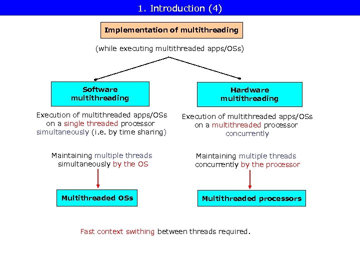 1. Introduction (4) Implementation of multithreading (while executing multithreaded apps/OSs) Software multithreading Hardware multithreading Execution of multithreaded apps/OSs on a single threaded processor simultaneously (i. e. by time sharing) Execution of multithreaded apps/OSs on a multithreaded processor concurrently Maintaining multiple threads simultaneously by the OS Maintaining multiple threads concurrently by the processor Multithreaded OSs Multithreaded processors Fast context swithing between threads required.
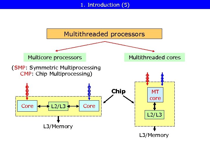 1. Introduction (5) Multithreaded processors Multicore processors Multithreaded cores (SMP: Symmetric Multiprocessing CMP: Chip Multiprocessing) Chip Core L 2/L 3 MT core Core L 2/L 3 L 3/Memory
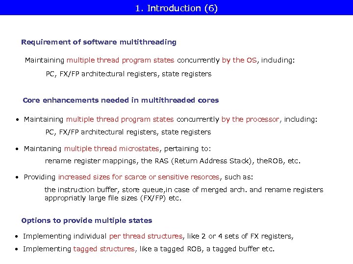 1. Introduction (6) Requirement of software multithreading Maintaining multiple thread program states concurrently by the OS, including: PC, FX/FP architectural registers, state registers Core enhancements needed in multithreaded cores • Maintaining multiple thread program states concurrently by the processor, including: PC, FX/FP architectural registers, state registers • Maintaning multiple thread microstates, pertaining to: rename register mappings, the RAS (Return Address Stack), the. ROB, etc. • Providing increased sizes for scarce or sensitive resorces, such as: the instruction buffer, store queue, in case of merged arch. and rename registers appropriatly large file sizes (FX/FP) etc. Options to provide multiple states • Implementing individual per thread structures, like 2 or 4 sets of FX registers, • Implementing tagged structures, like a tagged ROB, a tagged buffer etc.
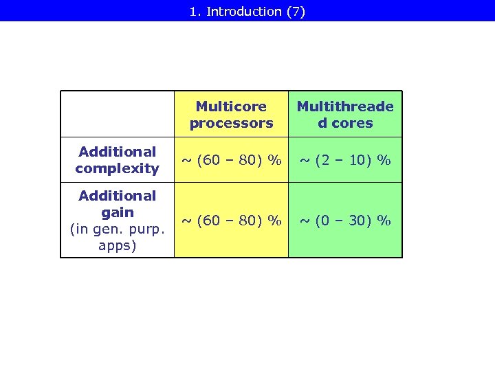 1. Introduction (7) Multicore processors Multithreade d cores Additional complexity ~ (60 – 80) % ~ (2 – 10) % Additional gain (in gen. purp. apps) ~ (60 – 80) % ~ (0 – 30) %
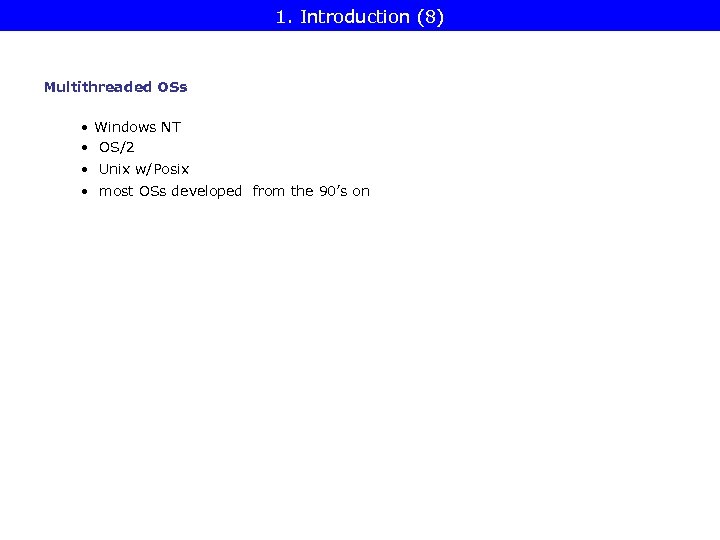 1. Introduction (8) Multithreaded OSs • Windows NT • OS/2 • Unix w/Posix • most OSs developed from the 90’s on
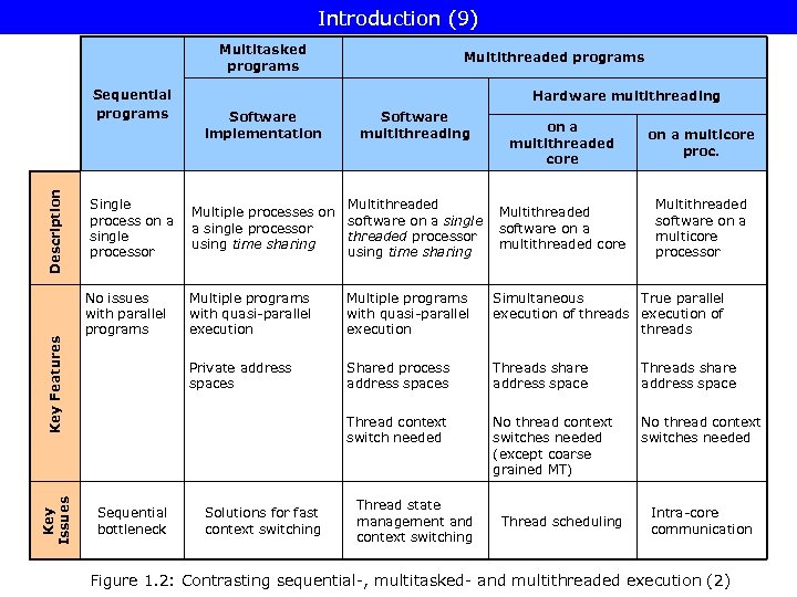 Introduction (9) Multitasked programs Key Issues Key Features Description Sequential programs Single process on a single processor No issues with parallel programs Multithreaded programs Hardware multithreading Software implementation Software multithreading Multithreaded Multiple processes on software on a single processor threaded processor using time sharing on a multithreaded core on a multicore proc. Multithreaded software on a multithreaded core Multithreaded software on a multicore processor Multiple programs with quasi-parallel execution Simultaneous True parallel execution of threads Private address spaces Shared process address spaces Threads share address space Thread context switch needed Sequential bottleneck Multiple programs with quasi-parallel execution No thread context switches needed (except coarse grained MT) No thread context switches needed Solutions for fast context switching Thread state management and context switching Thread scheduling Intra-core communication Figure 1. 2: Contrasting sequential-, multitasked- and multithreaded execution (2)
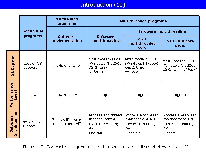 Introduction (10) Multitasked programs Software multithreading Legacy OS support Traditional Unix Most modern OS’s (Windows NT/2000, OS/2, Unix w/Posix) Low-medium Higher Highest Process and thread management API Explicit threading API Open. MP Software Development Software implementation OS Support Hardware multithreading Performance Level Sequential programs Multithreaded programs No API level support Process life cycle management API on a multithreaded core on a multicore proc. Most modern OS’s (Windows NT/2000, OS/2, Unix w/Posix) Figure 1. 3: Contrasting sequential-, multitasked- and multithreaded execution (2)
 2. Overview of multithreaded cores
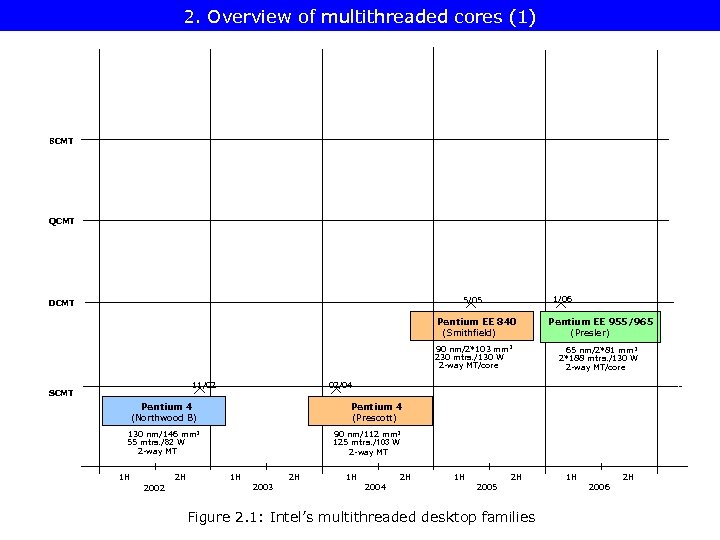 2. Overview of multithreaded cores (1) 8 CMT QCMT 1/06 5/05 DCMT Pentium EE 840 (Smithfield) 90 nm/2*103 mm 2 230 mtrs. /130 W 2 -way MT/core 11/02 SCMT Pentium EE 955/965 (Presler) 65 nm/2*81 mm 2 2*188 mtrs. /130 W 2 -way MT/core 02/04 Pentium 4 (Northwood B) Pentium 4 (Prescott) 130 nm/146 mm 2 55 mtrs. /82 W 2 -way MT 90 nm/112 mm 2 125 mtrs. /103 W 2 -way MT 1 H 2 H 2002 1 H 2 H 2003 1 H 2 H 2004 1 H 2 H 2005 Figure 2. 1: Intel’s multithreaded desktop families 1 H 2 H 2006
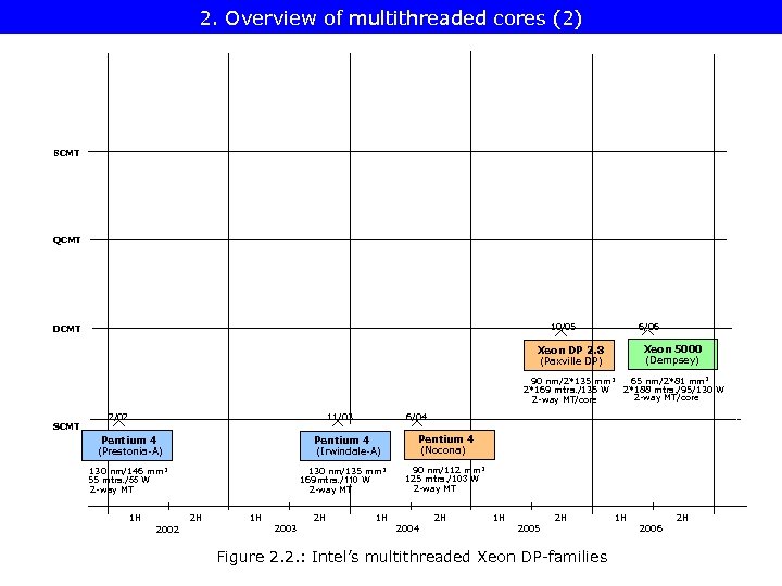 2. Overview of multithreaded cores (2) 8 CMT QCMT 6/06 10/05 DCMT Xeon 5000 (Dempsey) Xeon DP 2. 8 (Paxville DP) 65 nm/2*81 mm 2 90 nm/2*135 mm 2 2*188 mtrs. /95/130 W 2*169 mtrs. /135 W 2 -way MT/core SCMT 2/02 11/03 Pentium 4 (Prestonia-A) Pentium 4 (Irwindale-A) 130 nm/146 mm 2 55 mtrs. /55 W 2 -way MT 1 H 130 nm/135 mm 2 169 mtrs. /110 W 2 -way MT 2 H 2002 6/04 1 H 2 H 2003 Pentium 4 (Nocona) 90 nm/112 mm 2 125 mtrs. /103 W 2 -way MT 1 H 2 H 2004 1 H 2 H 2005 Figure 2. 2. : Intel’s multithreaded Xeon DP-families 1 H 2 H 2006
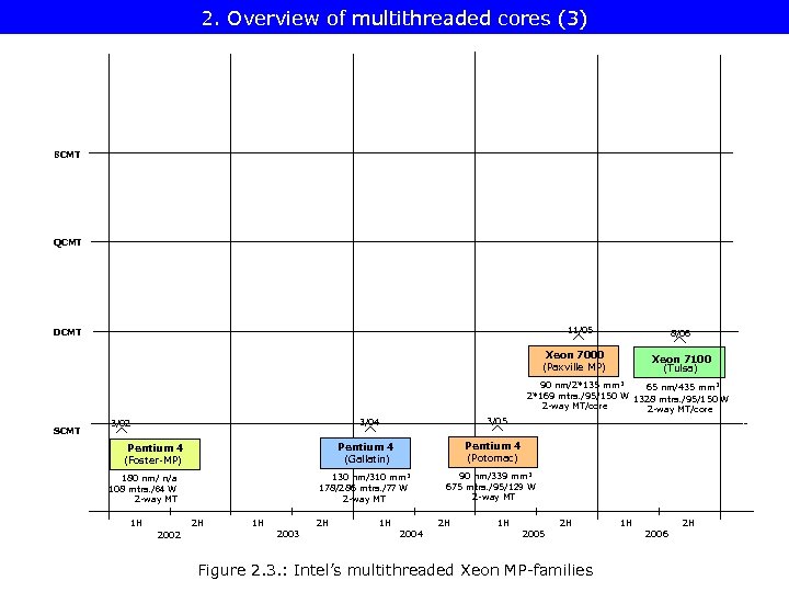 2. Overview of multithreaded cores (3) 8 CMT QCMT 11/05 DCMT 8/06 Xeon 7000 (Paxville MP) Xeon 7100 (Tulsa) 90 nm/2*135 mm 2 65 nm/435 mm 2 2*169 mtrs. /95/150 W 1328 mtrs. /95/150 W 2 -way MT/core SCMT 3/05 3/04 3/02 Pentium 4 (Gallatin) Pentium 4 (Potomac) 130 nm/310 mm 2 178/286 mtrs. /77 W 2 -way MT 90 nm/339 mm 2 675 mtrs. /95/129 W 2 -way MT Pentium 4 (Foster-MP) 180 nm/ n/a 108 mtrs. /64 W 2 -way MT 1 H 2 H 2002 1 H 2 H 2003 1 H 2 H 2004 1 H 2 H 2005 Figure 2. 3. : Intel’s multithreaded Xeon MP-families 1 H 2 H 2006
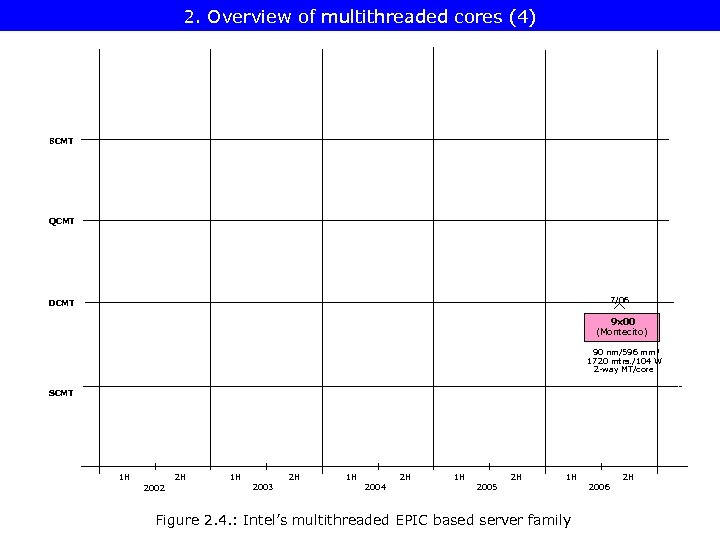 2. Overview of multithreaded cores (4) 8 CMT QCMT 7/06 DCMT 9 x 00 (Montecito) 90 nm/596 mm 2 1720 mtrs. /104 W 2 -way MT/core SCMT 1 H 2 H 2002 1 H 2 H 2003 1 H 2 H 2004 1 H 2 H 1 H 2005 Figure 2. 4. : Intel’s multithreaded EPIC based server family 2 H 2006
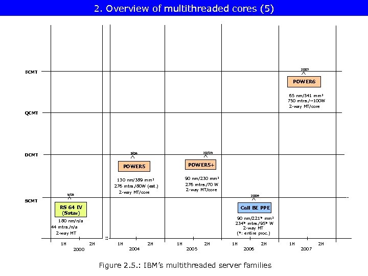 2. Overview of multithreaded cores (5) 2007 8 CMT POWER 6 65 nm/341 mm 2 750 mtrs. /~100 W 2 -way MT/core QCMT 10/05 5/04 DCMT POWER 5+ POWER 5 90 nm/230 mm 2 276 mtrs. /70 W 2 -way MT/core 130 nm/389 mm 2 276 mtrs. /80 W (est. ) 2 -way MT/core 5/04 2006 SCMT RS 64 IV (Sstar) Cell BE PPE 90 nm/221* mm 2 234* mtrs. /95* W 2 -way MT (*: entire proc. ) 180 nm/n/a 44 mtrs. /n/a 2 -way MT 1 H 2 H 2000 ~ ~ 1 H 2 H 2004 1 H 2 H 2005 1 H 2 H 2006 Figure 2. 5. : IBM’s multithreaded server families 1 H 2 H 2007
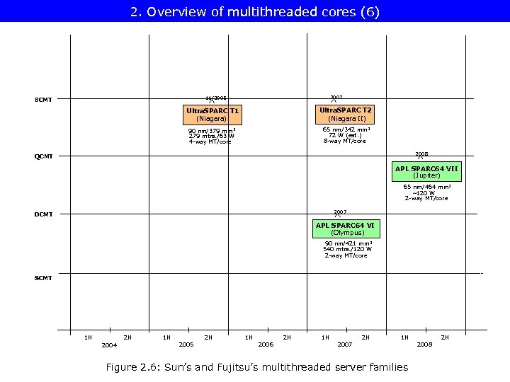 2. Overview of multithreaded cores (6) 2007 11/2005 8 CMT Ultra. SPARC T 1 (Niagara) Ultra. SPARC T 2 (Niagara II) 90 nm/379 mm 2 279 mtrs. /63 W 4 -way MT/core 65 nm/342 mm 2 72 W (est. ) 8 -way MT/core 2008 QCMT APL SPARC 64 VII (Jupiter) 65 nm/464 mm 2 ~120 W 2 -way MT/core 2007 DCMT APL SPARC 64 VI (Olympus) 90 nm/421 mm 2 540 mtrs. /120 W 2 -way MT/core SCMT 1 H 2 H 2004 1 H 2 H 2005 1 H 2 H 2006 1 H 2 H 1 H 2007 Figure 2. 6: Sun’s and Fujitsu’s multithreaded server families 2 H 2008
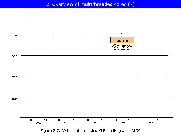 2. Overview of multithreaded cores (7) 5/05 8 CMT XLR 5 xx 90 nm/~220 mm 2 333 mtrs. /10 -50 W 4 -way MT/core QCMT DCMT SCMT 1 H 2 H 2002 1 H 2 H 2003 1 H 2 H 2004 1 H 2 H 2005 Figure 2. 7: RMI’s multithreaded XLR family (scalar RISC) 1 H 2 H 2006
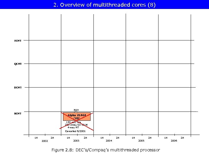 2. Overview of multithreaded cores (8) 8 CMT QCMT DCMT 2003 SCMT Alpha 21464 (V 8) 130 nm/ n/a 250 mtrs. /10 -50 W 4 -way MT Cancelled 6/2001 1 H 2 H 2002 1 H 2 H 2003 1 H 2 H 2004 1 H 2 H 2005 Figure 2. 8: DEC’s/Compaq’s multithreaded processor 1 H 2 H 2006
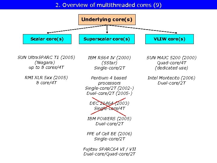 2. Overview of multithreaded cores (9) Underlying core(s) Scalar core(s) Superscalar core(s) VLIW core(s) SUN Ultra. SPARC T 1 (2005) (Niagara) up to 8 cores/4 T IBM RS 64 IV (2000) (SStar) Single-core/2 T SUN MAJC 5200 (2000) Quad-core/4 T (dedicated use) RMI XLR 5 xx (2005) 8 core/4 T Pentium 4 based processors Single-core/2 T (2002 -) Dual-core/2 T (2005 -) Intel Montecito (2006) Dual-core/2 T DEC 21464 (2003) Single-core/4 T IBM POWER 5 (2005) Dual-core/2 T PPE of Cell BE (2006) Single-core/2 T Fujitsu SPARC 64 VI / VII Dual-core/Quad-core/2 T
 3. Thread scheduling
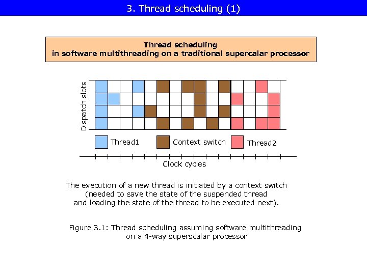 3. Thread scheduling (1) Dispatch slots Thread scheduling in software multithreading on a traditional supercalar processor Thread 1 Context switch Thread 2 Clock cycles The execution of a new thread is initiated by a context switch (needed to save the state of the suspended thread and loading the state of the thread to be executed next). Figure 3. 1: Thread scheduling assuming software multithreading on a 4 -way superscalar processor
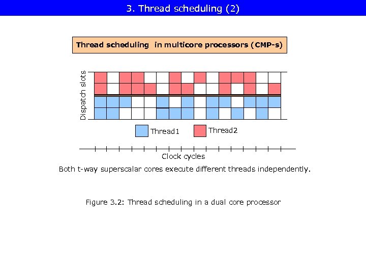 3. Thread scheduling (2) Dispatch slots Thread scheduling in multicore processors (CMP-s) Thread 1 Thread 2 Clock cycles Both t-way superscalar cores execute different threads independently. Figure 3. 2: Thread scheduling in a dual core processor
 3. Thread scheduling (3) Thread scheduling in multithreaded cores Coarse grained MT
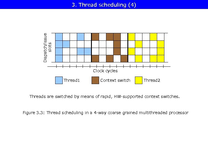 Dispatch/issue slots 3. Thread scheduling (4) Clock cycles Thread 1 Context switch Thread 2 Threads are switched by means of rapid, HW-supported context switches. Figure 3. 3: Thread scheduling in a 4 -way coarse grained multithreaded processor
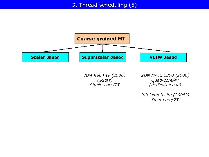 3. Thread scheduling (5) Coarse grained MT Scalar based Superscalar based IBM RS 64 IV (2000) (SStar) Single-core/2 T VLIW based SUN MAJC 5200 (2000) Quad-core/4 T (dedicated use) Intel Montecito (2006? ) Dual-core/2 T
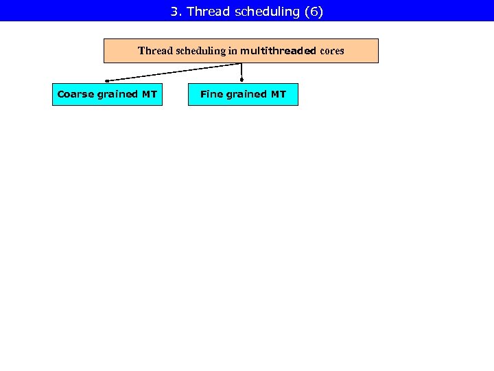 3. Thread scheduling (6) Thread scheduling in multithreaded cores Coarse grained MT Fine grained MT
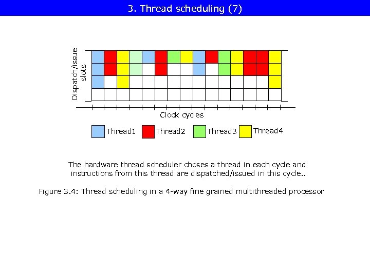 Dispatch/issue slots 3. Thread scheduling (7) Clock cycles Thread 1 Thread 2 Thread 3 Thread 4 The hardware thread scheduler choses a thread in each cycle and instructions from this thread are dispatched/issued in this cycle. . Figure 3. 4: Thread scheduling in a 4 -way fine grained multithreaded processor
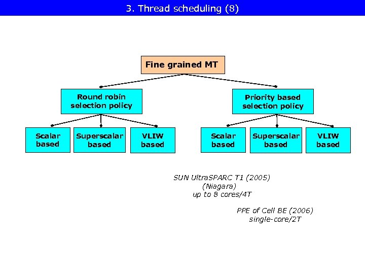 3. Thread scheduling (8) Fine grained MT Round robin selection policy Scalar based Superscalar based Priority based selection policy VLIW based Scalar based Superscalar based SUN Ultra. SPARC T 1 (2005) (Niagara) up to 8 cores/4 T PPE of Cell BE (2006) single-core/2 T VLIW based
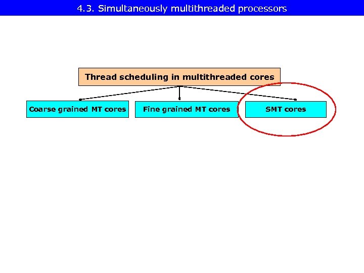
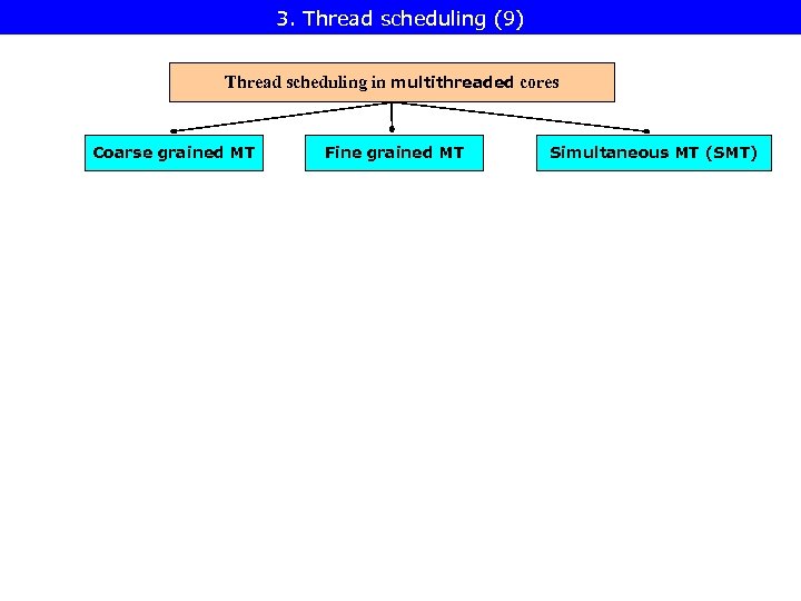 3. Thread scheduling (9) Thread scheduling in multithreaded cores Coarse grained MT Fine grained MT Simultaneous MT (SMT)
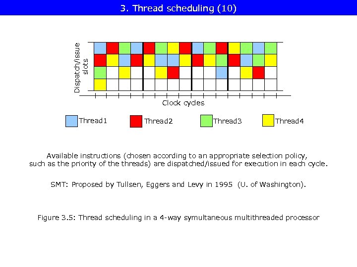 Dispatch/issue slots 3. Thread scheduling (10) Clock cycles Thread 1 Thread 2 Thread 3 Thread 4 Available instructions (chosen according to an appropriate selection policy, such as the priority of the threads) are dispatched/issued for execution in each cycle. SMT: Proposed by Tullsen, Eggers and Levy in 1995 (U. of Washington). Figure 3. 5: Thread scheduling in a 4 -way symultaneous multithreaded processor
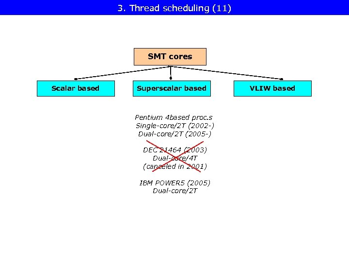 3. Thread scheduling (11) SMT cores Scalar based Superscalar based Pentium 4 based proc. s Single-core/2 T (2002 -) Dual-core/2 T (2005 -) DEC 21464 (2003) Dual-core/4 T (canceled in 2001) IBM POWER 5 (2005) Dual-core/2 T VLIW based
 4. Case examples 4. 1. Coarse grained multithreading 4. 2. Fine grained multithreading 4. 3. SMT multithreading
 4. 1 Coarse grained multithreaded processors 4. 1. 1. IBM RS 64 IV 4. 1. 2. SUN MAJC 5200 4. 1. 3. Intel Montecito
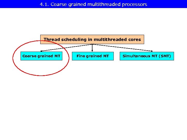 4. 1. Coarse grained multithreaded processors Thread scheduling in multithreaded cores Coarse grained MT Fine grained MT Simultaneous MT (SMT)
 4. 1. 1. IBM RS 64 IV (1) Microarchitecture 4 -way superscalar, dual-threaded. Used in IBM’s i. Series and p. Series commercial servers. Optimized for commercial server workloads, such as on-line transaction processing, Web-serving, ERP (Enterprise Resource Planning). Characteristics of server workloads: • • • large working sets, poor locality of references and frequently occurring task switches • high cache miss rates, • Memory bandwidth and latency strongly limits performance. need for wide instruction and data fetch bandwidth, need for large L 1 $s, using multithreading to hide memory latency.
 4. 1. 1. IBM RS 64 IV (2) Main microarchitectural features of the RS 64 IV to support commercial workloads: • 128 KB L 1 D$ and L 1 I$, • instruction fetch width: 8 instr. /cycle, • dual-threaded core.
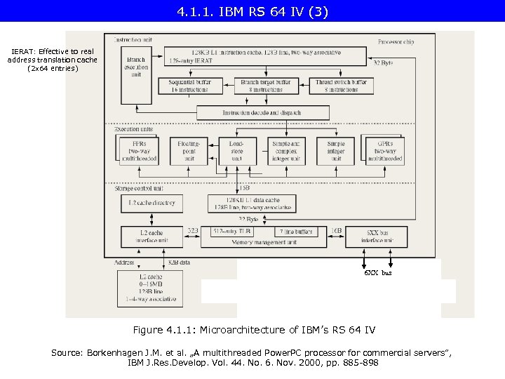 4. 1. 1. IBM RS 64 IV (3) IERAT: Effective to real address translation cache (2 x 64 entries) 6 XX bus Figure 4. 1. 1: Microarchitecture of IBM’s RS 64 IV Source: Borkenhagen J. M. et al. „A multithreaded Power. PC processor for commercial servers”, IBM J. Res. Develop. Vol. 44. No. 6. Nov. 2000, pp. 885 -898
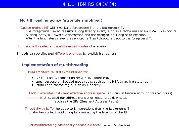 4. 1. 1. IBM RS 64 IV (4) Multithreading policy (strongly simplified) Coarse grained MT with two Ts; a foreground T and a background T. The foreground T executes until a long latency event, such as a cache miss or an IERAT miss occurs. Subsequently, a T switch is performed and the background T begins to execute. After the long latency event is serviced, a T switch occurs back to the foreground T. Both single threaded and multithreaded modes of execution. Threads can be allocated different priorities by explicit instructions. Implementation of multithreading Dual architectural states maintained for: • GPRs, FPRs, CR (condition reg. ), CTR (count reg. ), • spec. purpose priviledged mode reg. s, such as the MSR (machine state reg. . ) • status and control reg. s, such as T priority. Each T executes in its own effective address space (an unusual feature of multithreaded cores). Units used for address translation need to be duplicated, such as the SRs (Segment Address Reg. s) Thread Swith Buffer holds up to 8 instructions from the background T, to shorten context swithching by eliminating the latency of the I$ For multithreading additionally needed die area: ~ + 5 % die area
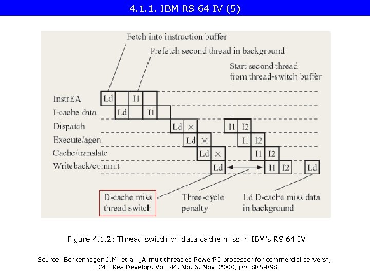 4. 1. 1. IBM RS 64 IV (5) Figure 4. 1. 2: Thread switch on data cache miss in IBM’s RS 64 IV Source: Borkenhagen J. M. et al. „A multithreaded Power. PC processor for commercial servers”, IBM J. Res. Develop. Vol. 44. No. 6. Nov. 2000, pp. 885 -898
 4. 1. 2. SUN MAJC 5200 (1) Aim: Dedicated use, high-end graphics, networking with wire-speed computational demands. Microarchitecture: • up to 4 processors on a die, • each processor has 4 FUs (Functional Units); 3 of them are identical, one is enhanced, • each FU has its private logic and register set (e. g. 32 or 64 regs. , • the 4 FUs of a processor share a set of global regs. , e. g. 64 regs. , • all registers are unified (not splitted to FX/FP files), • any FU can process any data type. Each processor is a 4 -wide VLIW and can be 4 -way multithreaded.
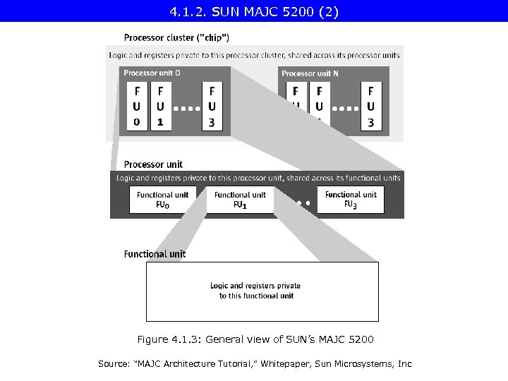 4. 1. 2. SUN MAJC 5200 (2) Figure 4. 1. 3: General view of SUN’s MAJC 5200 Source: “MAJC Architecture Tutorial, ” Whitepaper, Sun Microsystems, Inc
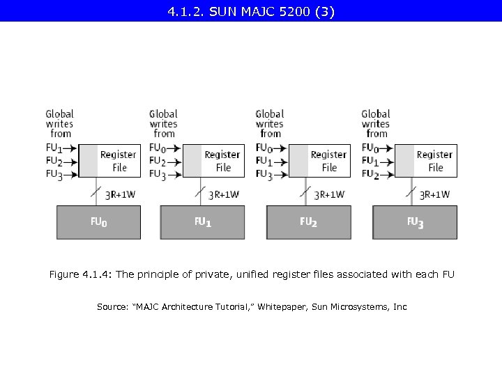 4. 1. 2. SUN MAJC 5200 (3) Figure 4. 1. 4: The principle of private, unified register files associated with each FU Source: “MAJC Architecture Tutorial, ” Whitepaper, Sun Microsystems, Inc
 4. 1. 2. SUN MAJC 5200 (4) Threading Each processor with its 4 FUs can be operated in a 4 -way multithreaded mode (called Vertical Multithreading by Sun) Implementation of 4 -way multithreading: by executing each T by one of the 4 FUs („Vertical multithreading”) Thread switch Following a cache miss, the processor saves the T state and begins to process the next T. Example Comparison of program execution without and with multithreading on a 4 -wide VLIW Considered program: • • It consists of 100 instructions, on average 2. 5 instrs. /cycle executed on average, giving birth to a cache miss after each 20 instructions. Latency of serving a cache miss: 75 cycles.
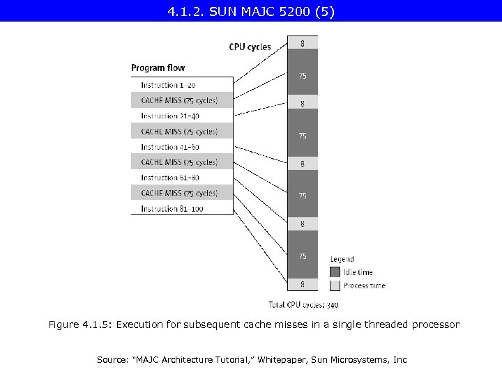 4. 1. 2. SUN MAJC 5200 (5) Figure 4. 1. 5: Execution for subsequent cache misses in a single threaded processor Source: “MAJC Architecture Tutorial, ” Whitepaper, Sun Microsystems, Inc
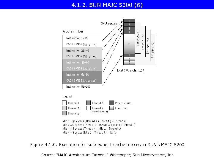 4. 1. 2. SUN MAJC 5200 (6) Figure 4. 1. 6: Execution for subsequent cache misses in SUN’s MAJC 5200 Source: “MAJC Architecture Tutorial, ” Whitepaper, Sun Microsystems, Inc
 4. 1. 3. Intel Montecito (1) Aim: High end servers Main differences between Itanium 2 and Montecito • • Split L 2 caches, larger unified L 3 cache, duplicated architectural states for FX/FP-registers, branch and predicate registers, next address register maintained. (Foxton technology for power management/frequency boost, planned but not implemented). Additional support for dual-threading (duplicated microarchitectural states) • • • the branch prediction structures provide T tagging, per thread return address stacks, per thread ALATs (Advance Load Address Table) Additional core area needed for multithreading: ~ 2 %.
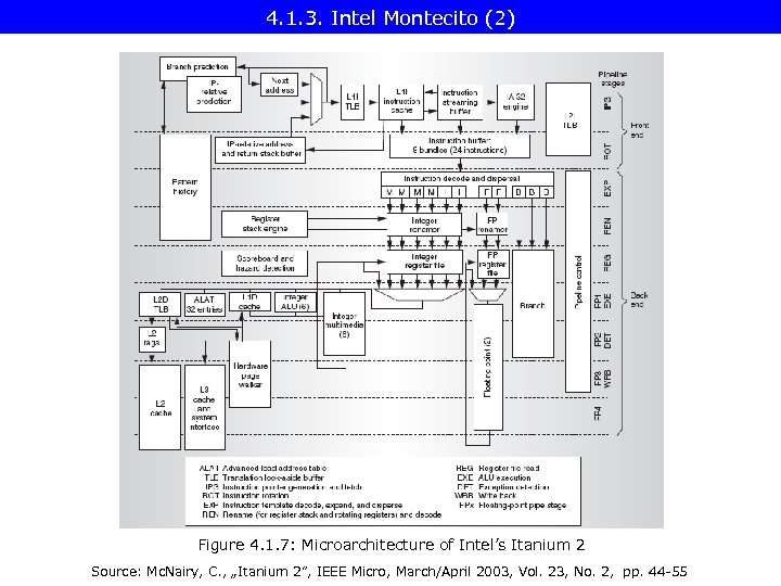 4. 1. 3. Intel Montecito (2) Figure 4. 1. 7: Microarchitecture of Intel’s Itanium 2 Source: Mc. Nairy, C. , „Itanium 2”, IEEE Micro, March/April 2003, Vol. 23, No. 2, pp. 44 -55
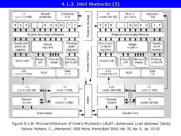 4. 1. 3. Intel Montecito (3) Figure 4. 1. 8: Microarchitecture of Intel’s Montecito (ALAT: Advanced Load Address Table) Source: Mc. Nairy, C. , „Montecito”, IEEE Micro, March/April 2005, Vol. 25, No. 2, pp. 10 -20
 4. 1. 3. Intel Montecito (4) Thread switches 5 event types cause thread switches, such as L 3 cache misses, programmed switched hints. Total switch penalty: 15 cycles Example for thread switching If control logic detects that a thread doesn’t make progress, a thread switch will be initiated.
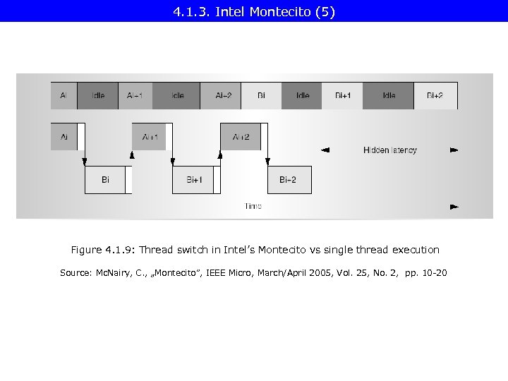 4. 1. 3. Intel Montecito (5) Figure 4. 1. 9: Thread switch in Intel’s Montecito vs single thread execution Source: Mc. Nairy, C. , „Montecito”, IEEE Micro, March/April 2005, Vol. 25, No. 2, pp. 10 -20
 4. 2 Fine grained multithreaded processors 4. 2. 1. SUN Ultrasparc T 1 4. 2. 2. PPE of Cell BE
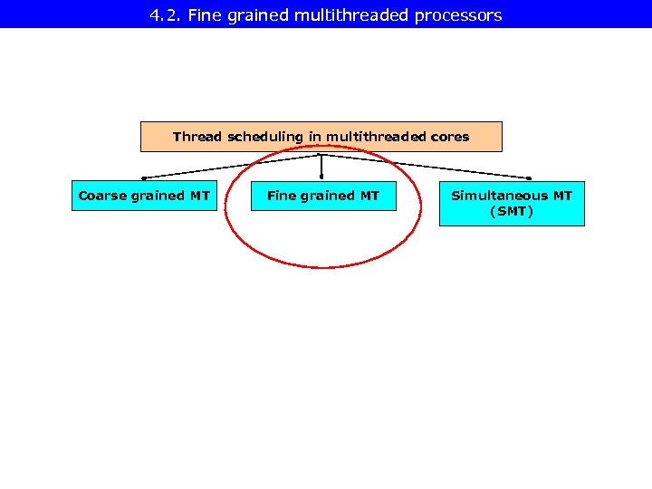 4. 2. Fine grained multithreaded processors Thread scheduling in multithreaded cores Coarse grained MT Fine grained MT Simultaneous MT (SMT)
 4. 2. 1. SUN Ultra. SPARC T 1 (1) Aim Commercial server applications, such as • • web servicing, transaction processing, ERP (Enterprise Resource Planning), DSS (Decision Support Systems) Characteristics of commercial server applications • large working sets, • poor locality of memory references. • high cache miss rates, • low prediction accuracy for data dependent branches. Memory latency strongly limits performance. Multithreading to hide memory latency.
 4. 2. 1. SUN Ultra. SPARC T 1 (2) Structure • 8 scalar cores, 4 -way multithreaded each. • All 32 threads share an L 2 cache of 3 MB, built up of 4 banks,
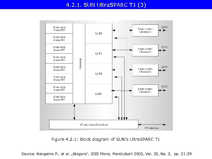 4. 2. 1. SUN Ultra. SPARC T 1 (3) Figure 4. 2. 1: Block diagram of SUN’s Ultra. SPARC T 1 Source: Kongetira P. , et al. „Niagara”, IEEE Micro, March/April 2005, Vol. 25, No. 2, pp. 21 -29
 4. 2. 1. SUN Ultra. SPARC T 1 (4) Structure • 8 scalar cores, 4 -way multithreaded each. • All 32 threads share an L 2 cache of 3 MB, built up of 4 banks, • 4 memory channels with on chip DDR 2 memory controllers. It runs under Solaris.
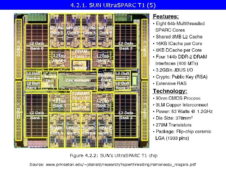 4. 2. 1. SUN Ultra. SPARC T 1 (5) Figure 4. 2. 2: SUN’s Ultra. SPARC T 1 chip Source: www. princeton. edu/~jdonald/research/hyperthreading/romanescu_niagara. pdf
 4. 2. 1. SUN Ultra. SPARC T 1 (6) Processor Elements (Sparc pipes): • Scalar FX-units, 6 -stage pipeline • all Processor Elements share a single FP-unit
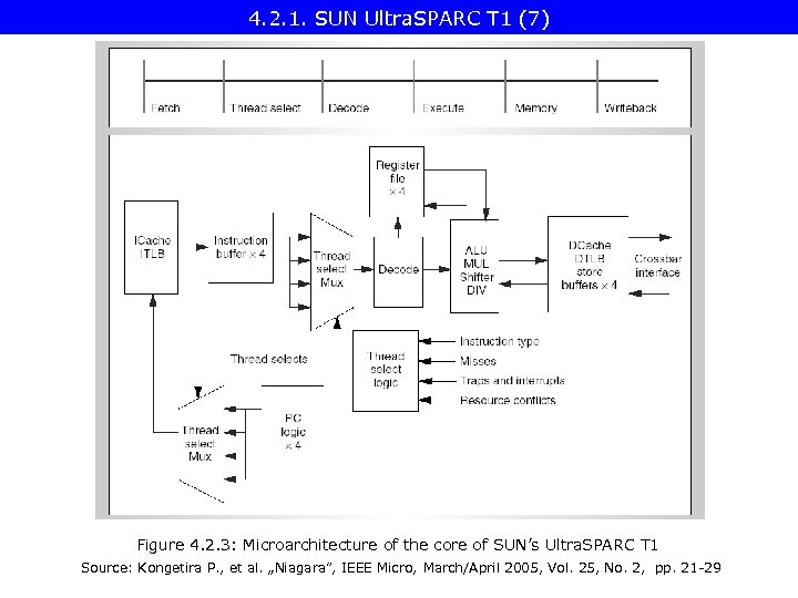 4. 2. 1. SUN Ultra. SPARC T 1 (7) Figure 4. 2. 3: Microarchitecture of the core of SUN’s Ultra. SPARC T 1 Source: Kongetira P. , et al. „Niagara”, IEEE Micro, March/April 2005, Vol. 25, No. 2, pp. 21 -29
 4. 2. 1. SUN Ultra. SPARC T 1 (8) Processor Elements (Sparc pipes): • Scalar FX-units, 6 -stage pipeline • all Processor Elements share a single FP-unit Each thread of a processor element has its private: • • PC-logic register file, instruction buffer, store buffer.
 4. 2. 1. SUN Ultra. SPARC T 1 (9) Figure 4. 2. 4: Microarchitecture of the core of SUN’s Ultra. SPARC T 1 Source: Kongetira P. , et al. „Niagara”, IEEE Micro, March/April 2005, Vol. 25, No. 2, pp. 21 -29
 4. 2. 1. SUN Ultra. SPARC T 1 (10) Processor Elements (Sparc pipes): • Scalar FX-units, 6 -stage pipeline • all Processor Elements share a single FP-unit Each thread of a processor element has its private: • • PC-logic, register file, instruction buffer, store buffer. No thread switch penalty!
 4. 2. 1. SUN Ultra. SPARC T 1 (11) Thread switch: Threads are switched on a per cycle basis. Selection of threads: In the thread select pipeline stage • the thread select multiplexer selects a thread from the set of available threads in each clock cycle and issues the subsequent instr. of this thread from the instruction buffer into the pipeline for execution, and • fetches the following instr. of the same thread into the instruction buffer.
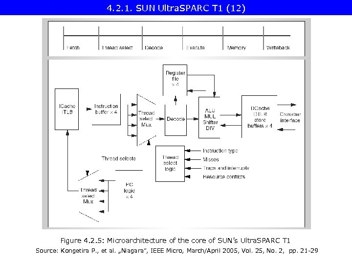 4. 2. 1. SUN Ultra. SPARC T 1 (12) Figure 4. 2. 5: Microarchitecture of the core of SUN’s Ultra. SPARC T 1 Source: Kongetira P. , et al. „Niagara”, IEEE Micro, March/April 2005, Vol. 25, No. 2, pp. 21 -29
 4. 2. 1. SUN Ultra. SPARC T 1 (13) Thread switch: Threads are switched on a per cycle basis. Selection of threads: In the thread select pipeline stage • the thread select multiplexer selects a thread from the set of available threads in each clock cycle and issues the subsequent instr. of this thread from the instruction buffer into the pipeline for execution, and • fetches the following instr. of the same thread into the instruction buffer. Thread selection policy: the least recently used policy. Threads become unavailable due to: • long-latency instructions, such as loads, branches, multiplies, divides, • pipeline stalls because of cache misses, traps, resource conflicts. 1. Example: • all 4 threads are available.
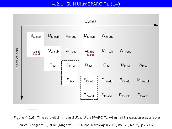 4. 2. 1. SUN Ultra. SPARC T 1 (14) t 0 -add t 1 -sub Figure 4. 2. 6: Thread switch in the SUN’s Ultra. SPARC T 1 when all threads are available Source: Kongetira P. , et al. „Niagara”, IEEE Micro, March/April 2005, Vol. 25, No. 2, pp. 21 -29
 4. 2. 1. SUN Ultra. SPARC T 1 (15) 2. Example: • There are only 2 threads available, • speculative execution of instructions following a load. (Data referenced by a load instruction arrive in the 3. cycle after decoding, assuming a cache hit. So, after issuing a load the thread becomes unavailable for the next two subsequent cycles. )
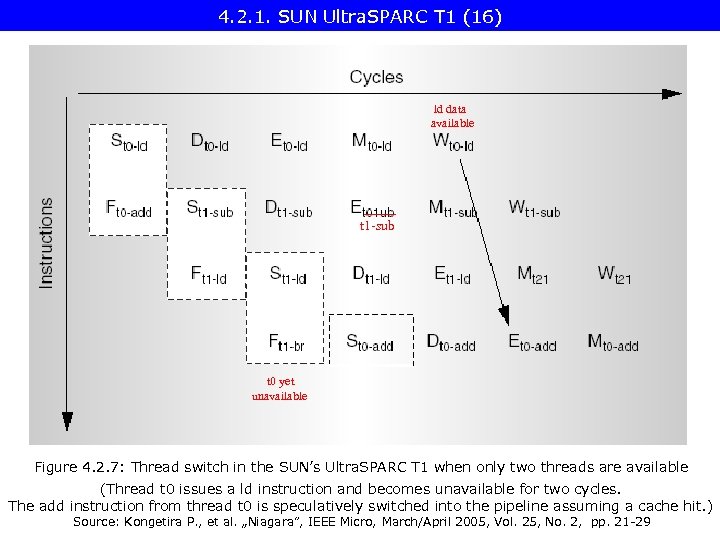 4. 2. 1. SUN Ultra. SPARC T 1 (16) ld data available t 1 -sub t 0 yet unavailable Figure 4. 2. 7: Thread switch in the SUN’s Ultra. SPARC T 1 when only two threads are available (Thread t 0 issues a ld instruction and becomes unavailable for two cycles. The add instruction from thread t 0 is speculatively switched into the pipeline assuming a cache hit. ) Source: Kongetira P. , et al. „Niagara”, IEEE Micro, March/April 2005, Vol. 25, No. 2, pp. 21 -29
 4. 2. 2. Cell BE Ø Overview of the Cell BE Ø Processor components Ø Multithreading the PPE Ø Programming models Ø Implementation of the Cell BE
 Overview of the Cell BE (1) Cell BE Objective: Speeding up game/multimedia apps. Used: In the Play. Station 3 (PS 3) and in the QS 20 Blade Server Goal: 100 times the PS 2 performance. History CELL BE: Collaborative effort from Sony, IBM and Toshiba Summer 2000: End 2000: March 2001: Spring 2004: Summer 2004: Febr. 2005: Oct. 2005: Nov. 2005: Febr. 2006: High level architectural discussions Architectural concept Design Center opened in Austin TX. Single Cell BE operational 2 -way SMP operational First technical disclosures Mercury announces Cell Blade Open Source SDK & Simulator published IBM announced Cell Blade QS 20 Cell BE at NIK May 2007: QS 20 arrives at NIK within IBM’s loan program
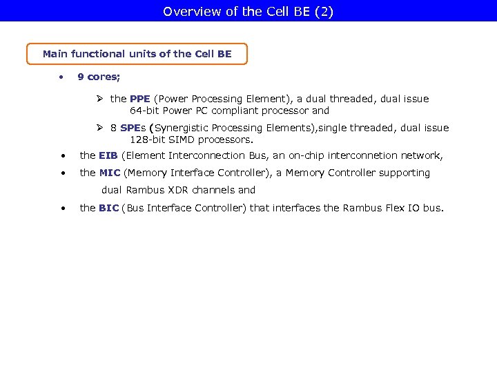 Overview of the Cell BE (2) Main functional units of the Cell BE • 9 cores; Ø the PPE (Power Processing Element), a dual threaded, dual issue 64 -bit Power PC compliant processor and Ø 8 SPEs (Synergistic Processing Elements), single threaded, dual issue 128 -bit SIMD processors. • the EIB (Element Interconnection Bus, an on-chip interconnetion network, • the MIC (Memory Interface Controller), a Memory Controller supporting dual Rambus XDR channels and • the BIC (Bus Interface Controller) that interfaces the Rambus Flex IO bus.
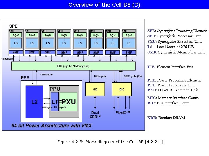 Overview of the Cell BE (3) SPE: Synergistic Procesing Element SPU: Synergistic Processor Unit SXU: Synergistic Execution Unit LS: Local Store of 256 KB SMF: Synergistic Mem. Flow Unit EIB: Element Interface Bus PPE: Power Processing Element PPU: Power Processing Unit PXU: POWER Execution Unit MIC: Memory Interface Contr. BIC: Bus Interface Contr. XDR: Rambus DRAM Figure 4. 2. 8: Block diagram of the Cell BE [4. 2. 2. 1]
 Overview of the Cell BE (4) Unique features of the Cell BE a) Heterogeneous MCP rather than being a symmetrical MCP (as usual implementations) The PPE • is optimized to run a 32/64 -bit OS • controls usually the SPEs, • complies with the 64 -bit Power. PC ISA. The SPEs • are optimized to run compute intensive SIMD apps. , • operate usually under the control of the PPE, • run their individual apps. (threads), • have full access to a coherent shared memory including the memory mapped I/O-space, • can be programmed in C/C++. Contrasting the PPE and the SPEs • the PPE is more adept at control-intensive tasks and quicker in task switching, • the SPEs are more adept at compute intensive tasks and slower at task switcing.
 Overview of the Cell BE (5) b) The SPEs have an unusual storage architecture, as • SPEs Ø operate in connection with a local store (LS) of 256 KB, i. e. o they fetch instructions from their private LS and o their Load/Store-instructions access their LS rather than the main store, • The LS Ø has no associated cache. • SPEs Ø access main memory (effective address space) by DMA commands, i. e. DMA commands move data and instructions between main store and the private LS, while Ø DMA commands can be batched (up to 16 commands).
 Overview of the Cell BE (6) Although the PPE and the SPEs have coherent access to main memory, the Cell BE is not a traditional shared-memory multiprocessor as SPEs operate in connnection with the LS rather than with the main memory.
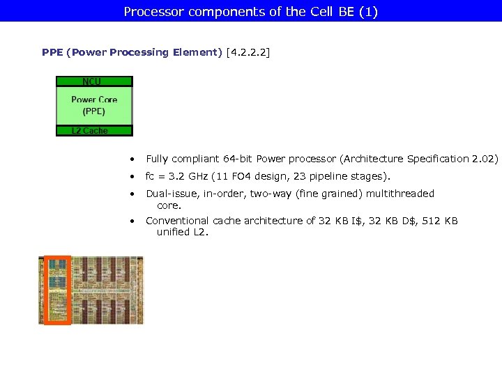 Processor components of the Cell BE (1) PPE (Power Processing Element) [4. 2. 2. 2] • Fully compliant 64 -bit Power processor (Architecture Specification 2. 02) • fc = 3. 2 GHz (11 FO 4 design, 23 pipeline stages). • Dual-issue, in-order, two-way (fine grained) multithreaded core. • Conventional cache architecture of 32 KB I$, 32 KB D$, 512 KB unified L 2.
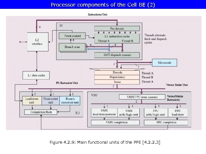 Processor components of the Cell BE (2) Instructions Unit FX Execution Unit Vector Scalar Unit Vector/Media Execution) Figure 4. 2. 9: Main functional units of the PPE [4. 2. 2. 3]
 Processor components of the Cell BE (3) Main components of the PPE • IU (Instruction unit) Ø predecodes instructions while loading them from the L 2 cache to the L 1 cache, Ø fetches 4 instructions per cycle alternating between the two threads from the L 1 instr. cache into two instruction buffers (each one for each thread), Ø dispatches instructions from the two instruction buffers to the shared decode, dependency checking and issue pipeline according to the thread scheduling rules. • Microcode Engine Ø Instructions that are either difficult to implement in hardware or are rarely used can be split into a few simple Power. PC instructions and are stored in a ROM (such as Load string or several Condition Register (CR) instructions. Ø Most microcoded instructions are split into two or three microcoded instruction. Ø The Microcode Engine inserts microcoded instructions from one thread into the instruction flow with a delay of 11 clock cycles. Ø The Microcode Engine stalls dispatching from the instruction buffers until the last microcode of the microcoded instruction is dispatched. Ø The next dispatch cycle belongs to the thread that did not invoke the Microcode Engine. • Shared decode, dependency checking and issue pipeline Ø Receives dispatched instructions (up to two in each cycle from the same thread), Ø it decodes them, checks for dependencies, and issues instructions for execution according to the issue rules.
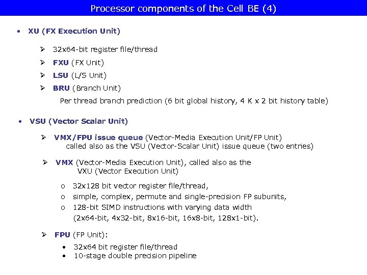 Processor components of the Cell BE (4) • XU (FX Execution Unit) Ø 32 x 64 -bit register file/thread Ø FXU (FX Unit) Ø LSU (L/S Unit) Ø BRU (Branch Unit) Per thread branch prediction (6 bit global history, 4 K x 2 bit history table) • VSU (Vector Scalar Unit) Ø VMX/FPU issue queue (Vector-Media Execution Unit/FP Unit) called also as the VSU (Vector-Scalar Unit) issue queue (two entries) Ø VMX (Vector-Media Execution Unit), called also as the VXU (Vector Execution Unit) o o o Ø 32 x 128 bit vector register file/thread, simple, complex, permute and single-precision FP subunits, 128 -bit SIMD instructions with varying data width (2 x 64 -bit, 4 x 32 -bit, 8 x 16 -bit, 16 x 8 -bit, 128 x 1 -bit). FPU (FP Unit): • • 32 x 64 bit register file/thread 10 -stage double precision pipeline
 Processor components of the Cell BE (5) Basic operation of the PPE Instr. fetch • Instruction fetch operates autonomously in order to keep each thread’s instruction buffer full with useful instructions that are likely to be needed. • 4 instr. /cycle are fetched strictly alternating between the two threads from the L 1 I$ to the private Instruction Buffers of the threads. • The fetch address is taken from the Instruction Fetch Address Registers associated with each thread (IFAR 0, IFAR 1). The IFARs are distinct from the Program Counters (PC) associated with both threads; the PCs track the actual program flow while the IFARs track the predicted instruction execution flow. • Accessing the taken path after a predicted-taken branch requires 8 cycles.
 Processor components of the Cell BE (6) Instruction dispatch • Moves up to two instructions either Ø Ø from one of the Instruction Buffers or the Microcode Engine (complex instructions) to the shared decode, dependency check and issue pipeline. • Instruction dispatch is governed by the dispatch rules (thread scheduling rules). • The dispatch rules take into account thread priority and stall conditions (see Section 5. 34? ). • Each pipeline stage beyond the dispath point contains instructions from one thread only. Instruction decode and dependency checking Decoding of up to two instructions from the same tread in each cycle and checking for dependencies
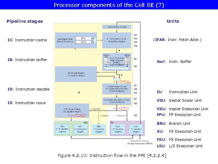 Processor components of the Cell BE (7) Pipeline stages Units (IFAR: Instr. Fetch Addr. ) IC: Instruction cache 4 IB: Instruction buffer ibuf: Instr. Buffer 2 ID: Instruction decode IS: Instruction issue IU: Instruction Unit VSU: Vector Scalar Unit VXU: Vector Execution Unit FPU: FP Execution Unit BRU: Branch Unit XU: FX Execution Unit FXU: FX Execution Unit LSU: L/S Execution Unit Figure 4. 2. 10: Instruction flow in the PPE [4. 2. 2. 4]
 Processor components of the Cell BE (8) Instruction issue at the pipeline stage IS 2 • Forwarding up to two Power. PC or vector/SIMD multimedia extension instructions per cycle from the IS 2 pipeline stage for execution to the Ø Ø • VSU (VMX/FPU) issue queue (up to two instr. /cycle) or the BRU, LSU, FXU execution units (up to one instr. /cycle per execution unit). Any issue combinations are allowed, except two instructions to the same unit with a few restrictions. (See Figure 4. 2. 11 for the valid issue combinations. ) Note that valid resp. invalid issue combinations result from the underlying microarchitecture, as shown in Figure 4. 2. 13. • Instructions are issued in each cycle from the same thread. • Instruction issue can be stalled at the IS 2 pipeline stage for various reasons, like invalid issue combinations, full VSU issue queue. Instruction issue from the VSU (VMX/FPU) issue queue Forwarding up to two VMX or FPU instructions to the respective execution units. Note that instructions kept in the issue queue are already prearranged for execution, i. e. they obey the issue restrictions summarized in Figure 4. 2. 11.
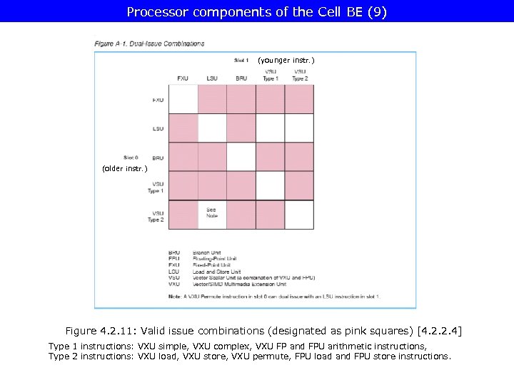 Processor components of the Cell BE (9) (younger instr. ) (older instr. ) Figure 4. 2. 11: Valid issue combinations (designated as pink squares) [4. 2. 2. 4] Type 1 instructions: VXU simple, VXU complex, VXU FP and FPU arithmetic instructions, Type 2 instructions: VXU load, VXU store, VXU permute, FPU load and FPU store instructions.
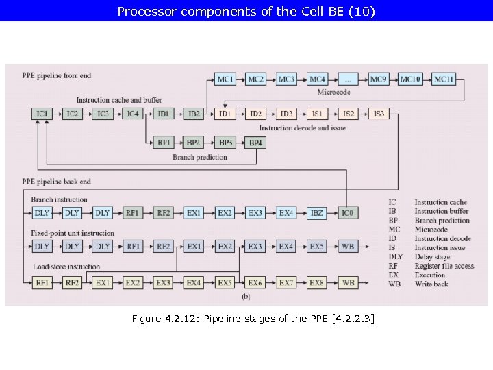 Processor components of the Cell BE (10) Figure 4. 2. 12: Pipeline stages of the PPE [4. 2. 2. 3]
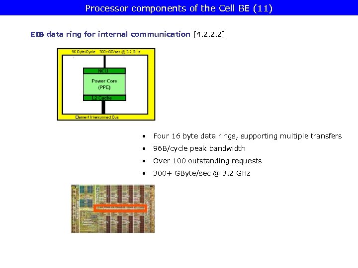 Processor components of the Cell BE (11) EIB data ring for internal communication [4. 2. 2. 2] • Four 16 byte data rings, supporting multiple transfers • 96 B/cycle peak bandwidth • Over 100 outstanding requests • 300+ GByte/sec @ 3. 2 GHz
![Processor components of the Cell BE (12) SPE [4. 2. 2. 2] • SPEs Processor components of the Cell BE (12) SPE [4. 2. 2. 2] • SPEs](https://present5.com/presentation/ac15cc7ebff202d89491e34cd230b138/image-91.jpg) Processor components of the Cell BE (12) SPE [4. 2. 2. 2] • SPEs optimized for data-rich operation • are allocated by the PPE • SPEs are not intended to run an OS Main Components a) SPU (Synergistic Processing Unit) b) MFC (Memory Flow Controller) c) LS (Local Store) d) AUC (Atomic Unit and Cache) SPE
Processor components of the Cell BE (12) SPE [4. 2. 2. 2] • SPEs optimized for data-rich operation • are allocated by the PPE • SPEs are not intended to run an OS Main Components a) SPU (Synergistic Processing Unit) b) MFC (Memory Flow Controller) c) LS (Local Store) d) AUC (Atomic Unit and Cache) SPE
 Processor components of the Cell BE (13) a) SPU Overview • Dual-issue superscalar RISC core supporting basically a 128 -bit SIMD ISA. • The SIMD ISA provides FX, FP and logical operations on 2 x 64 -bit, 4 x 32 -bit, 8 x 16 -bit, 16 x 8 -bit and 128 x 1 -bit data. • In connnection with the MFC the SPU support also a set of commands for - performing DMA transfers, - interprocessor messaging and - synchronization. • The SPU executes instructions from the LS (256 KB), • Instructions reference data from the 128 x 128 -bit unified register file, • The Register file fetches/delivers data from/to the LS by L/S instructions, • The SPU moves instructions and data between the main memory and the local store by requesting DMA transfers from its MFC. (Up to 16 outstanding DMA requests allowed).
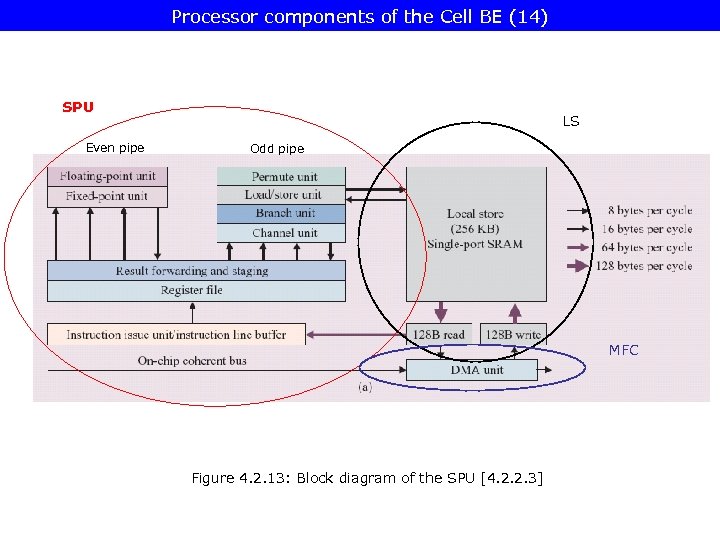 Processor components of the Cell BE (14) SPU Even pipe LS Odd pipe MFC Figure 4. 2. 13: Block diagram of the SPU [4. 2. 2. 3]
 Processor components of the Cell BE (15) Main components of the SPU • Instruction issue unit – instruction line buffer Ø Fetches 32 instructions per LS request from the LS into the Instruction line buffer. Ø Instruction fetching is supported by hardware prefetching. Pefetching requires 15 cycles to fill the instruction line buffer. Ø Fetched instructions are decoded and issued (up to two instructions per cycle) according to the issue rules. • Register file Ø Unified Register file of 128 registers each 128 -bit wide. • Result forwarding and staging Ø Instructions are staged in an operand staging network for up to 6 additinal cycles to achieve that all execution units write their results in the Register file in the same pipeline stage. (See Figure 4. 2. 19).
 Processor components of the Cell BE (16) • Execution units are organised into two pipelines. Ø The even pipeline includes o the Fixed-point unit and o the Floating-point unit. Ø The o o odd pipeline includes the Channel unit, Branch unit, Load/Store unit and the Permute unit.
 Processor components of the Cell BE (17) Basic operation of the SPU Instruction issue • The SPU issues up to two instructions per cycle from a 2 -instructions wide issue window, called the fetch group. • Fetch groups are aligned to doubleword boundaries, i. e. the first instruction is at an even and the second one at an odd word address. (Words are 4 -Byte long). • An instruction becomes issueable when no register dependencies or resource conflicts, e. g. busy execution units, exist. • Instructions are issued in program order, that is - if the first instruction of a fetch group can be issued to the even pipeline and the second instruction to the odd pipeline both instructions are issued in the same cycle, - in all other cases instruction issue needs two cycles such that instructions are issued in program order to the pertaining pipeline (see Figure 4. 2. 14). • Register or resource conflicts stall instruction issue. • A new fetch group is loaded after both instructions of the current fetch group are issued.
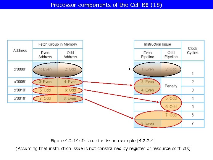 Processor components of the Cell BE (18) Figure 4. 2. 14: Instruction issue example [4. 2. 2. 4] (Assuming that instruction issue is not constrained by register or resource conflicts)
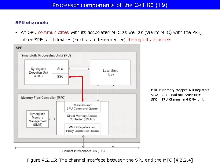 Processor components of the Cell BE (19) SPU channels • An SPU communicates with its associated MFC as well as (via its MFC) with the PPE, other SPEs and devices (such as a decrementer) through its channels. MMIO: Memory-Mapped I/O Registers SLC: SPU Load and Store Unit SSC: SPU Channel and DMA Unit Figure 4. 2. 15: The channel interface between the SPU and the MFC [4. 2. 2. 4]
 Processor components of the Cell BE (20) • SPU channels are unidirectional interfaces for Ø Ø • sending commands (such as DMA commands) to the MFC, owned by the SPU or sending/receiving up to 32 -bit long messages between the SPU and the PPE or other SPEs. SPU channels are implemented in and managed by the MFC. • Each channel has - a corresponding capacity (maximum message entries) and - count (remaining available message entries). The channel count - decrements when ever a channel instruction (rdch or wrch)is issued, and - increments whenever an operation associated with the channnel completes. The channel count of „ 0” means - empty for read only channels and - full for write only channels.
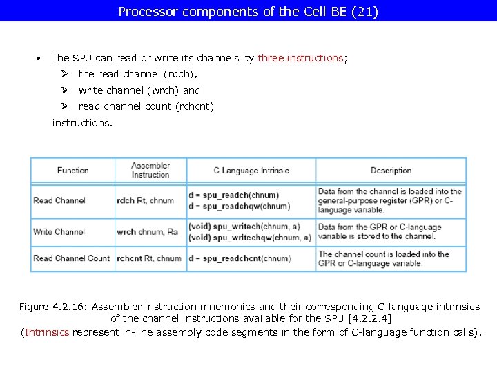 Processor components of the Cell BE (21) • The SPU can read or write its channels by three instructions; Ø the read channel (rdch), Ø write channel (wrch) and Ø read channel count (rchcnt) instructions. Figure 4. 2. 16: Assembler instruction mnemonics and their corresponding C-language intrinsics of the channel instructions available for the SPU [4. 2. 2. 4] (Intrinsics represent in-line assembly code segments in the form of C-language function calls).
 Processor components of the Cell BE (22) • The channel instructions or DMA commands evoked by channel instructions are enqueued for execution in the MFC for purposes like Ø initiating DMA transfers between the SPE’s LS and the main storage, Ø queuring DMA and SPU status, Ø sending or receiving up to 32 -bit long mailbox messages primarily between the SPU and the PPE or Ø sending or receiving up to 32 -bit long signal-notification messages between the SPU and the PPE or other SPEs. • The PPE and other devices in the system including other SPEs, can also access the channels through the MFC’s memory mapped I/O (MMIO) registers and queues, which are visible to software in the main storage space.
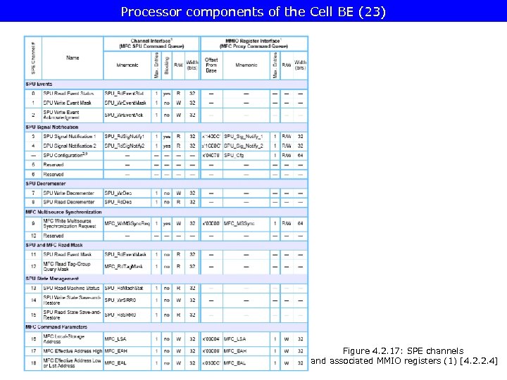 Processor components of the Cell BE (23) Figure 4. 2. 17: SPE channels and associated MMIO registers (1) [4. 2. 2. 4]
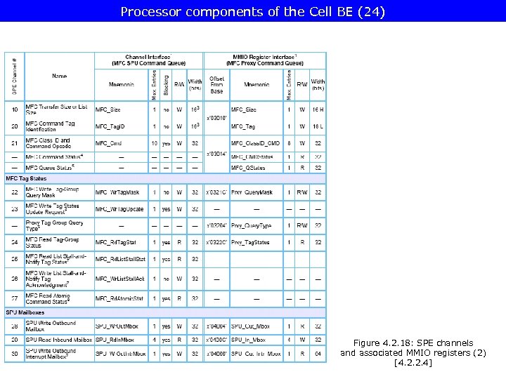 Processor components of the Cell BE (24) Figure 4. 2. 18: SPE channels and associated MMIO registers (2) [4. 2. 2. 4]
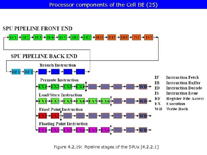 Processor components of the Cell BE (25) Figure 4. 2. 19: Pipeline stages of the SPUs [4. 2. 2. 1]
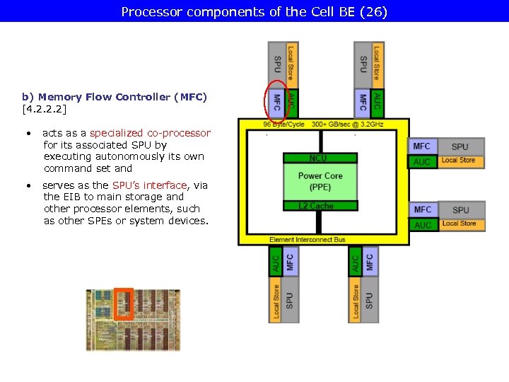 Processor components of the Cell BE (26) b) Memory Flow Controller (MFC) [4. 2. 2. 2] • acts as a specialized co-processor for its associated SPU by executing autonomously its own command set and • serves as the SPU’s interface, via the EIB to main storage and other processor elements, such as other SPEs or system devices.
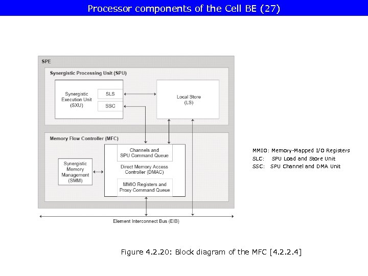 Processor components of the Cell BE (27) MMIO: Memory-Mapped I/O Registers SLC: SPU Load and Store Unit SSC: SPU Channel and DMA Unit Figure 4. 2. 20: Block diagram of the MFC [4. 2. 2. 4]
 Processor components of the Cell BE (28) The MFC as a specialized co-processor It executes three types of commands • DMA List commands and • synchronization commands. • DMA commands (put, get) • can be initaiated by both the PPE and the SPU, • move up to 16 KByte of data between the LS and the main storage, • supports transfer sizes of 1, 2, 4, 8. 16 bytes and multiples of 16 bytes, • access main store by using main storage effective addresses, • can be tagged with a 5 -bit tag (tag group ID) to allow special handling within the tag group, such a to enforce ordering of the DMA commands. • DMA list commands (put, get commands with the command modifier l) • can be initiated only by the SPU, • consist of up to 2 K 8 -byte long list elements, • each list element specifies a DMA transfer • used to move data between a contiguous area in the LS and possible noncontiguous area in the effective address space implementing scatter-gather functions between main storage and the LS).
 Processor components of the Cell BE (29) • Synchronization comands • used basically to control the order of storage accesses, • include atomic commands (a form of semaphores), send signal commands and barrier commands. Operation of the MFC • The MFC maintains two separate command queues - • the 16 -entry SPU comand queue for commands from the SPU associated with the MFC, and the 8 -entry proxi command queue for commands from the PPE, other SPEs and devices. The MFC supports out-of-order execution of DMA commands.
 Processor components of the Cell BE (30) The MFC as the interface between the SPU and the main storage, the PPE and other devices • supports storage protection on the main storage side while performing DMA transfers, • maintains synchronization between main storage and the LS, • performs intercore communication functions, such as mailbox and signal-notification messaging with the PPE, other SPEs and devices.
 Processor components of the Cell BE (31) Intercore communication tools of the MFC • three mailboxes, primarily intended for holding up to 32 -bit long messages from/to the SPE: - • one four-deep mailbox for receiving mailbox messages and two one-deep mailbox for sending mailbox messages. two signal notification channels for receiving signals sent basically by the PPE.
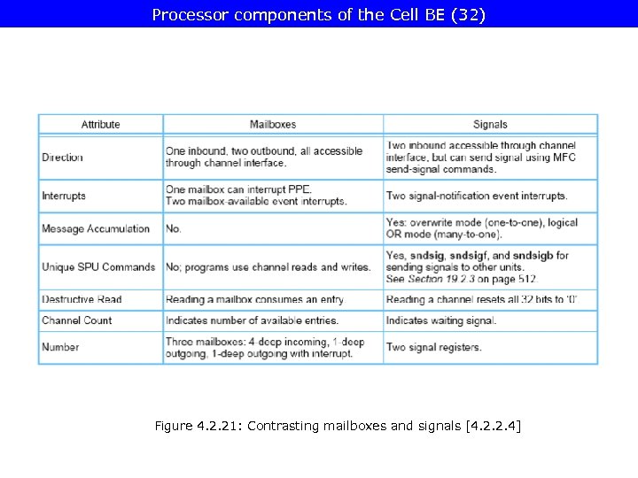 Processor components of the Cell BE (32) Figure 4. 2. 21: Contrasting mailboxes and signals [4. 2. 2. 4]
![Processor components of the Cell BE (33) c) Local Store [4. 2. 2. 2] Processor components of the Cell BE (33) c) Local Store [4. 2. 2. 2]](https://present5.com/presentation/ac15cc7ebff202d89491e34cd230b138/image-112.jpg) Processor components of the Cell BE (33) c) Local Store [4. 2. 2. 2] • Single-port SRAM cell. • Executes DMA reads/writes and instruction prefetches via 128 -Byte wide read/write ports • Executes instruction fetches and load/stores via 128 -bit read/write ports. • Asynchronous, coherent DMA commands are used to move instructions and data between the local store and system memory. • DMA transfers between the LS and the main storage are executed by the SMF’s DMA unit • A 128 -Byte long DMA read or write requires 16 processor cycles to forward data on the EIB. SPE
Processor components of the Cell BE (33) c) Local Store [4. 2. 2. 2] • Single-port SRAM cell. • Executes DMA reads/writes and instruction prefetches via 128 -Byte wide read/write ports • Executes instruction fetches and load/stores via 128 -bit read/write ports. • Asynchronous, coherent DMA commands are used to move instructions and data between the local store and system memory. • DMA transfers between the LS and the main storage are executed by the SMF’s DMA unit • A 128 -Byte long DMA read or write requires 16 processor cycles to forward data on the EIB. SPE
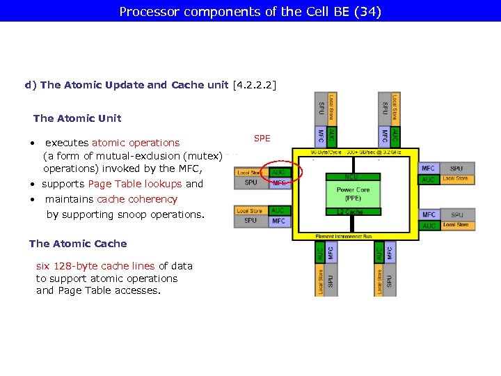 Processor components of the Cell BE (34) d) The Atomic Update and Cache unit [4. 2. 2. 2] The Atomic Unit • executes atomic operations (a form of mutual-exclusion (mutex) operations) invoked by the MFC, • supports Page Table lookups and • maintains cache coherency by supporting snoop operations. The Atomic Cache six 128 -byte cache lines of data to support atomic operations and Page Table accesses. SPE
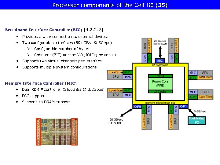 Processor components of the Cell BE (35) Broadband Interface Controller (BIC) [4. 2. 2. 2] • Provides a wide connection to external devices • Two configurable interfaces (50+GB/s @ 5 Gbps) Ø Configurable number of bytes Ø Coherent (BIF) and/or I/O (IOIFx) protocols • Supports two virtual channels per interface • Supports multiple system configurations Memory Interface Controller (MIC) • Dual XDRTM controller (25. 6 GB/s @ 3. 2 Gbps) • ECC support • Suspend to DRAM support
 Multithreading the PPE (1) Scheduling of PPE threads Thread scheduling depends both on • • thread states thread priorities • single threaded or dual threaded mode of execution
 Multithreading the PPE (2) 1. Thread states • Privilege states • Suspended/enabled state • Blocked/not blocked state a) Privilege States • Hypervisor state • most privileged • allows to run a meta OS that manages logical partitions in which multiple OS instances can run • some system operations require the initiating thread to be in hypervisor state • Supervisor state • • is the state in which an OS instance is intended to run Problem state (user state) • is the state in which an application is intended to rum
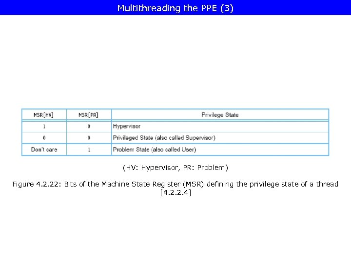 Multithreading the PPE (3) (HV: Hypervisor, PR: Problem) Figure 4. 2. 22: Bits of the Machine State Register (MSR) defining the privilege state of a thread [4. 2. 2. 4]
 Multithreading the PPE (4) b) Suspended/enabled State • a thread in the hypervisor state can change its state from enabled to suspended. • Two bits of the Control Register (CTRL[TE 0], [TE 1]) define whether a thread is in the suspended or enabled state. c) Blocked/stalled State • Blocking - occurs at the instruction dispatch stage if the thread selection rule favours the other thread, or due to a special „nop” instruction, - stops only one of the two threads. • Stalling - occurs at the instruction issue stage due to dependencies - stops both threads. - for very long latency conditions, such as L 1 cache misses, or devide instructions, stalling both threads is avoided, by -- flushing instructions younger than the stalled instruction, -- instructions starting with the stalled instruction are refetched and -- the thread is stalled at the dispatch stage until the stall condition is removed, but then the other thread can be continued to dispatch.
 Multithreading the PPE (5) 2. Thread priorities • determines dispatch priority • four priority levels thread disabled low priority medium priority high priorith • priority levels are specified by a 2 -bit field (TP field) of the TSRL register (Thread Status Regiter Local) • Software, in particular OS software, sets thread priorities (according to the throughput requirements of the programs running in the threads. ) E. g. a foreground/background thread priority scheme can be set, to favor one thread over the other when allocating instruction dispatch slots. • A thread must be in the hypervisor or supervisor state to set its priority to high.
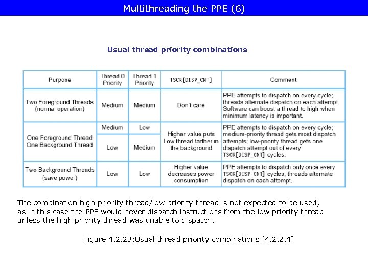 Multithreading the PPE (6) Usual thread priority combinations The combination high priority thread/low priority thread is not expected to be used, as in this case the PPE would never dispatch instructions from the low priority thread unless the high priority thread was unable to dispatch. Figure 4. 2. 23: Usual thread priority combinations [4. 2. 2. 4]
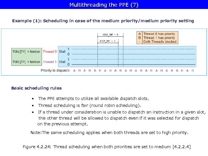 Multithreading the PPE (7) Example (1): Scheduling in case of the medium priority/medium priority setting Basic scheduling rules • The PPE attempts to utilize all available dispatch slots. • Thread scheduling is fair (round robin scheduling). • If a thread under consideration is unable to dispatch an instruction in a given slot, the other thread will be allowed to dispatch even if it was selected for dispatch on the previous attempt. Note: The same scheduling applies when both threads are set to high priority. Figure 4. 2. 24: Thread scheduling when both priorities are set to medium [4. 2. 2. 4]
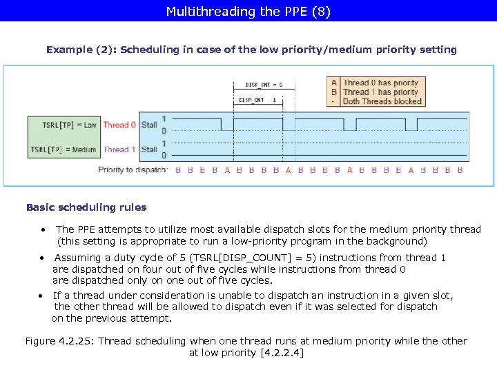 Multithreading the PPE (8) Example (2): Scheduling in case of the low priority/medium priority setting Basic scheduling rules • The PPE attempts to utilize most available dispatch slots for the medium priority thread (this setting is appropriate to run a low-priority program in the background) • Assuming a duty cycle of 5 (TSRL[DISP_COUNT] = 5) instructions from thread 1 are dispatched on four out of five cycles while instructions from thread 0 are dispatched only on one out of five cycles. • If a thread under consideration is unable to dispatch an instruction in a given slot, the other thread will be allowed to dispatch even if it was selected for dispatch on the previous attempt. Figure 4. 2. 25: Thread scheduling when one thread runs at medium priority while the other at low priority [4. 2. 2. 4]
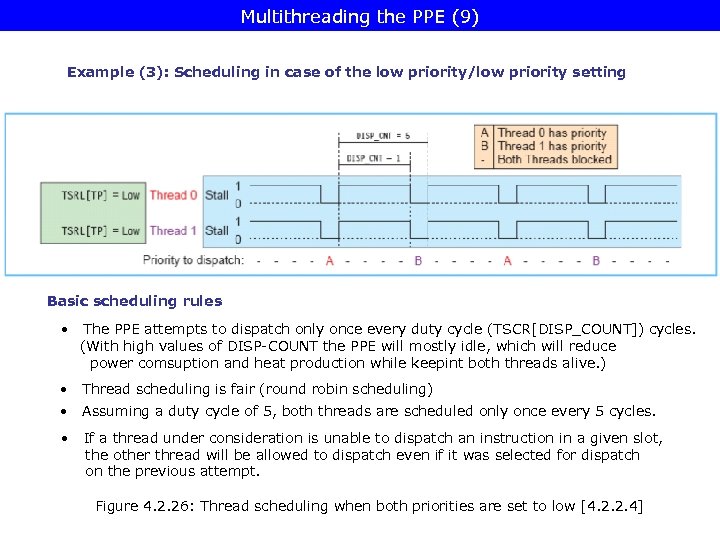 Multithreading the PPE (9) Example (3): Scheduling in case of the low priority/low priority setting Basic scheduling rules • The PPE attempts to dispatch only once every duty cycle (TSCR[DISP_COUNT]) cycles. (With high values of DISP-COUNT the PPE will mostly idle, which will reduce power comsuption and heat production while keepint both threads alive. ) • • Thread scheduling is fair (round robin scheduling) • If a thread under consideration is unable to dispatch an instruction in a given slot, the other thread will be allowed to dispatch even if it was selected for dispatch on the previous attempt. Assuming a duty cycle of 5, both threads are scheduled only once every 5 cycles. Figure 4. 2. 26: Thread scheduling when both priorities are set to low [4. 2. 2. 4]
 Multithreading the PPE (10) 3. Single threaded/dual threaded mode of execution • In single threaded mode all resources are allocated to a single thread, this reduces the turnaround time of the thread. • Software can change the operating mode of the PPE between single threaded and dual threaded mode only in the hypervisor state.
 Multithreading the PPE (11) Software controlled thread behaviour software can use various schemes to controll thread behaviour, including • enabling and suspending a thread, • • by setting thread priorities to control instruction dispatch policy, executing a special nop instruction to cause temporary dispatch blocking, • switching the state of the PPE between single threaded and multithreaded mode.
 Multithreading the PPE (12) Core enhancements for multithreading • Duplicated architectural states for 32 GPRs 32 FPRs 32 Vector Registers (VRs) Condition Register (CR) Count Register (CTR) Link Register (LR) FX Exception Register (XER) FP Status and Control Register (FPSCR) Vector Status and Control Register (VSCR) Decrementer (DEC)
 Multithreading the PPE (13) • Duplicated microarchitectural states for Branch History Table (BHT) with global branch history (to allow independent and simultaneous branch prediction for both threads) Internal registers associated with exceptions and interrupt handling, such as Machine State Register (MR) Machine Status Save/Restore Registers (SRR 0, SRR 1) Hipervisor Machine Status Save/Restore Registers (HSRR 0, HSRR 1) FP Status and Control Register (FPSCR) etc. (to allow concurrent exception and interrupt handling)
 Multithreading the PPE (14) • Duplicated queues and arrays Segment lookaside buffer (SLB) Instruction buffer queue (Ibuf) (to allow each thread to dispatch regardles of any dispatch stall in the other thread) Link stack queue • Shared resources Hardware execution units The instruction fetch control (because the I$ has only one read port and so fetching must alternate between threads every cycle). Virtual memory mapping (as both threads always execute in the same logical partitioning context) Most large arrays and queues, such as caches that consume significant amount of chip area
 Multithreading the PPE (15) The programming model assumes the choice of an appropriate SPU configuration Basic SPU configurations • Application specific SPU accelerators, • Multi-stage pipeline SPU configuration or • Parallel-stages SPU configuration;
![Multithreading the PPE (16) Application specific SPU accelerators [4. 2. 2. 5] Multithreading the PPE (16) Application specific SPU accelerators [4. 2. 2. 5]](https://present5.com/presentation/ac15cc7ebff202d89491e34cd230b138/image-130.jpg) Multithreading the PPE (16) Application specific SPU accelerators [4. 2. 2. 5]
Multithreading the PPE (16) Application specific SPU accelerators [4. 2. 2. 5]
![Multithreading the PPE (17) Multi-stage SPU pipeline configuration [4. 2. 2. 5] Multithreading the PPE (17) Multi-stage SPU pipeline configuration [4. 2. 2. 5]](https://present5.com/presentation/ac15cc7ebff202d89491e34cd230b138/image-131.jpg) Multithreading the PPE (17) Multi-stage SPU pipeline configuration [4. 2. 2. 5]
Multithreading the PPE (17) Multi-stage SPU pipeline configuration [4. 2. 2. 5]
![Programming models (1) Parallel-stages SPU configuration [4. 2. 2. 5] Programming models (1) Parallel-stages SPU configuration [4. 2. 2. 5]](https://present5.com/presentation/ac15cc7ebff202d89491e34cd230b138/image-132.jpg) Programming models (1) Parallel-stages SPU configuration [4. 2. 2. 5]
Programming models (1) Parallel-stages SPU configuration [4. 2. 2. 5]
 Programming models (2) Basic approach for creating an application • Programmer chooses the appropriate SPU configuration according to the features of an application, such as Ø Ø • Graphics processing Audio processing MPEG Encoding/Decoding Encryption/Decryption Programmer writes/uses SPU „libraries” either for Ø Ø Multi-stage pipeline SPU configuration or Ø • Application specific SPU accelerators, Parallel-stages SPU configuration; e. g. for; Main application in PPE, invokes SPU bound services by Ø creating SPU threads Ø RPC like function calls Ø I/O device like interfaces (FIFO/command queue) • One ore more SPUs cooperate in the presumed SPU configuration to execute the tasks required.
 Programming models (3) • Acceleration provided by OS or application libraries • Application portability maintained with platform specific libraries
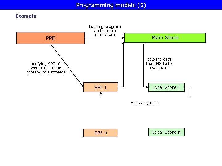
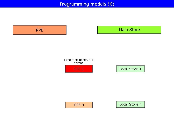
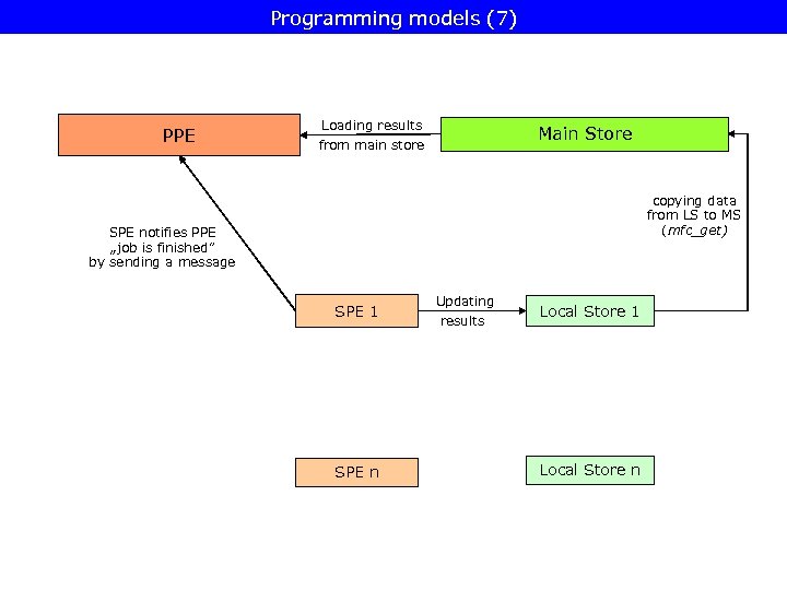
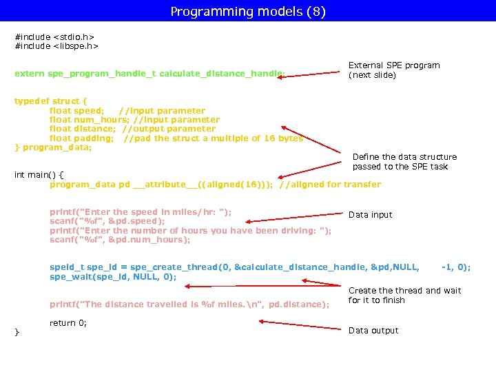
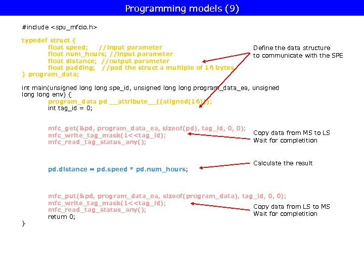
 Programming models (4) Example Aim • showing the cooperation between PPE and SPE Program • Actual goal: To calculate distance travelled in a car • It asks for: Ø elapsed time Ø speed Program structure • There are two program codes, one for the PPE and one for the SPE. • The PPE does the user input, then it calls the SPE executable which calculates the distance and then returns with the result. • The result is then given to the user by the PPE.
 Programming models (5) Example PPE Loading program and data to main store Main Store copying data from MS to LS (mfc_get) notifying SPE of work to be done (create_spu_thread) SPE 1 Local Store 1 Accessing data SPE n Local Store n
 Programming models (6) Main Store PPE Execution of the SPE thread SPE 1 Local Store 1 SPE n Local Store n
 Programming models (7) PPE Loading results from main store Main Store copying data from LS to MS (mfc_get) SPE notifies PPE „job is finished” by sending a message SPE 1 SPE n Updating results Local Store 1 Local Store n
 Programming models (8) #include
 Programming models (9) #include
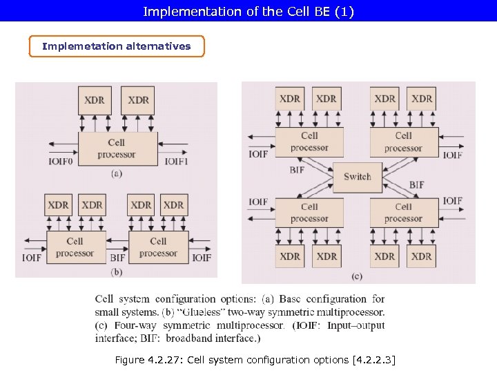 Implementation of the Cell BE (1) Implemetation alternatives Figure 4. 2. 27: Cell system configuration options [4. 2. 2. 3]
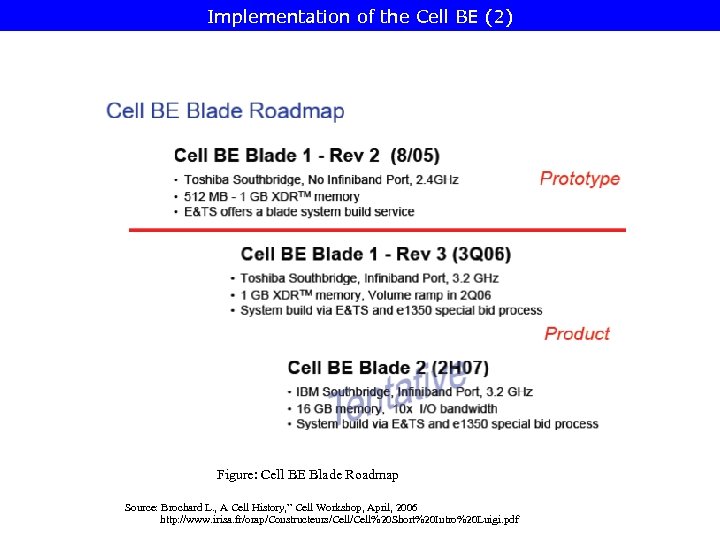 Implementation of the Cell BE (2) Figure: Cell BE Blade Roadmap Source: Brochard L. , A Cell History, ” Cell Workshop, April, 2006 http: //www. irisa. fr/orap/Constructeurs/Cell%20 Short%20 Intro%20 Luigi. pdf
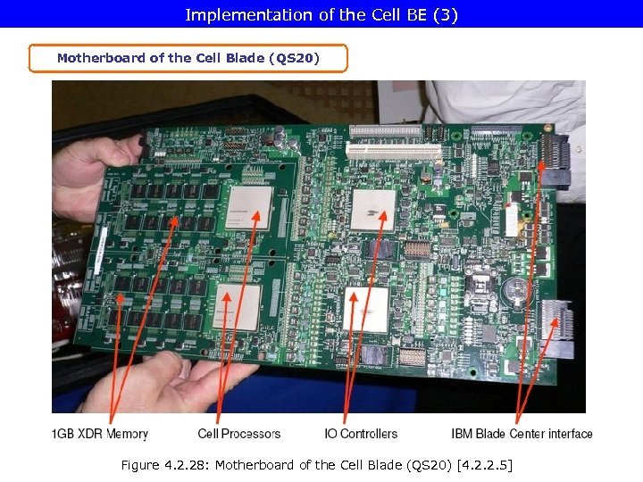 Implementation of the Cell BE (3) Motherboard of the Cell Blade (QS 20) Figure 4. 2. 28: Motherboard of the Cell Blade (QS 20) [4. 2. 2. 5]
![References Cell BE [4. 2. 2. 1] Gshwind M. , „Chip Multiprocessing and the References Cell BE [4. 2. 2. 1] Gshwind M. , „Chip Multiprocessing and the](https://present5.com/presentation/ac15cc7ebff202d89491e34cd230b138/image-144.jpg) References Cell BE [4. 2. 2. 1] Gshwind M. , „Chip Multiprocessing and the Cell BE, ” ACM Computing Frontiers, 2006, http: //beatys 1. mscd. edu/compfront//2006/cf 06 -gschwind. pdf [4. 2. 2. 2] Hofstee P. , „Tutorial: Hardware and Software Architectures for the CELL BROADBAND ENGINE processor”, IBM Corp. , September 2005 http: //www. crest. gatech. edu/conferences/cases 2005/pdf/Cell-tutorial. pdf [4. 2. 2. 3] Kahle J. A. , „Introduction to the Cell multiprocessor”, IBM J. Res & Dev Vol. 49, 2005, pp. 584 -604 http: //www. research. ibm. com/journal/rd/494/kahle. pdf [4. 2. 2. 4]: Cell Broadband Engine Programming Handbook Vers. 1. 1, Apr. 2007, IBM Corp. [4. 2. 2. 5] Cell BE Overview, Course code: L 1 T 1 H 1 -02, May 2006, IBM Corp.
References Cell BE [4. 2. 2. 1] Gshwind M. , „Chip Multiprocessing and the Cell BE, ” ACM Computing Frontiers, 2006, http: //beatys 1. mscd. edu/compfront//2006/cf 06 -gschwind. pdf [4. 2. 2. 2] Hofstee P. , „Tutorial: Hardware and Software Architectures for the CELL BROADBAND ENGINE processor”, IBM Corp. , September 2005 http: //www. crest. gatech. edu/conferences/cases 2005/pdf/Cell-tutorial. pdf [4. 2. 2. 3] Kahle J. A. , „Introduction to the Cell multiprocessor”, IBM J. Res & Dev Vol. 49, 2005, pp. 584 -604 http: //www. research. ibm. com/journal/rd/494/kahle. pdf [4. 2. 2. 4]: Cell Broadband Engine Programming Handbook Vers. 1. 1, Apr. 2007, IBM Corp. [4. 2. 2. 5] Cell BE Overview, Course code: L 1 T 1 H 1 -02, May 2006, IBM Corp.
 4. 3 SMT multithreaded processors 4. 3. 1. Intel Pentium 4 4. 3. 2. Alpha 21464 (V 8) 4. 3. 3. IBM Power 5
 4. 3. Simultaneously multithreaded processors Thread scheduling in multithreaded cores Coarse grained MT cores Fine grained MT cores SMT cores
 4. 3. 1. Intel Pentium 4 (1) Intel designates SMT as Hyperthreading (HT) Introduced in the Northwood based DP- and MP-server cores in 2/2002 and 3/2002 resp. (called the Prestonia and Foster MP cores), followed by the Northwood core for desktops in 11/2002. Additions for implementing MT: • Duplicated architectural state, including • • • instruction pointer, the general purpose regs. , the control regs. , the APIC (Advanced Programable Interrupt Controller) regs. , some machine state regs.
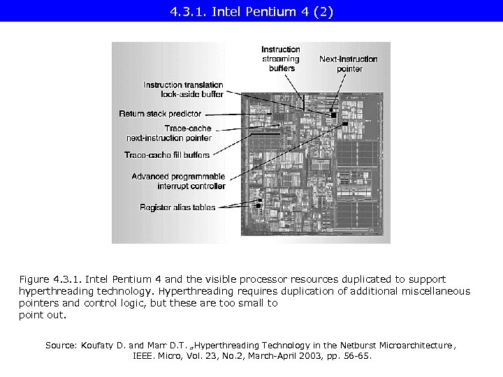 4. 3. 1. Intel Pentium 4 (2) Figure 4. 3. 1. Intel Pentium 4 and the visible processor resources duplicated to support hyperthreading technology. Hyperthreading requires duplication of additional miscellaneous pointers and control logic, but these are too small to point out. Source: Koufaty D. and Marr D. T. „Hyperthreading Technology in the Netburst Microarchitecture , IEEE. Micro, Vol. 23, No. 2, March-April 2003, pp. 56 -65.
 4. 3. 1. Intel Pentium 4 (3) Intel designates SMT as Hyperthreading (HT) Introduced in the Northwood based DP- and MP-server cores in 2/2002 and 3/2002 resp. (called the Prestonia and Foster MP cores), followed by the Northwood core for desktops in 11/2002. Additions for implementing MT: • Duplicated architectural state, including • • • instruction pointer, the general purpose regs. , the control regs. , the APIC (Advanced Programable Interrupt Controller) regs. , some machine state regs. • Further enhancements to support MT (thread microstate): • • • TC-entries (Trace cache) are tagged, BHB (Branch History Buffer) is duplicated, Global History Table is tagged, RAS (Return Address Stack) is duplicated, Rename tables are duplicated, ROB is tagged.
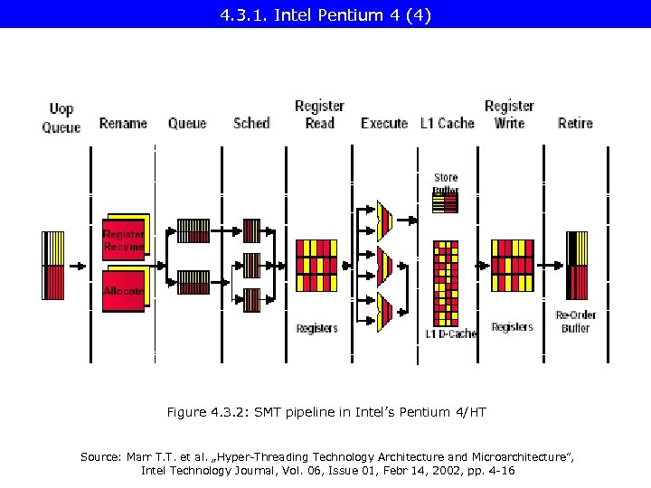 4. 3. 1. Intel Pentium 4 (4) Figure 4. 3. 2: SMT pipeline in Intel’s Pentium 4/HT Source: Marr T. T. et al. „Hyper-Threading Technology Architecture and Microarchitecture”, Intel Technology Journal, Vol. 06, Issue 01, Febr 14, 2002, pp. 4 -16
 4. 3. 1. Intel Pentium 4 (5) Intel designates SMT as Hyperthreading (HT) Introduced in the Northwood based DP- and MP-server cores in 2/2002 and 3/2002 resp. (called the Prestonia and Foster MP cores), followed by the Northwood core for desktops in 11/2002. Additions for implementing MT: • Duplicated architectural state, including • • • instruction pointer, the general purpose regs. , the control regs. , the APIC (Advanced Programable Interrupt Controller) regs. , some machine state regs. • Further enhancements to support MT (thread microstate): • • • TC-entries (Trace cache) are tagged, BHB (Branch History Buffer) is duplicated, Global History Table is tagged, RAS (Return Address Stack) is duplicated, Rename tables are duplicated, ROB is tagged. Additional die area required for MT: less than 5 %. Single thread/dual thread modes: To prevent single thread performance degradation: in single thred mode partitioned resources are recombined.
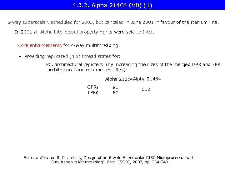 4. 3. 2. Alpha 21464 (V 8) (1) 8 -way superscalar, scheduled for 2003, but canceled in June 2001 in favour of the Itanium line. In 2001 all Alpha intellectual property rights were sold to Intel. Core enhancements for 4 -way multithreading: • Providing replicated (4 x) thread states for: PC, architectural registers (by increasing the sizes of the merged GPR and FPR architectural and rename reg. files): Alpha 21264 Alpha 21464 GPRs FPRs 80 80 512 Source: : Preston R. P. and all. , Design of an 8 -wide Superscalar RISC Microprocessor with Simultaneous Mltithreading”, Proc. ISSCC, 2002, pp. 334 -243
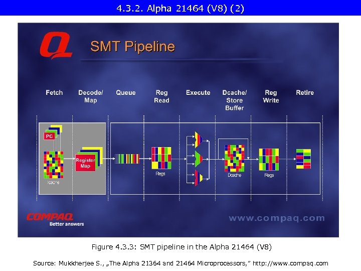 4. 3. 2. Alpha 21464 (V 8) (2) Figure 4. 3. 3: SMT pipeline in the Alpha 21464 (V 8) Source: Mukkherjee S. , „The Alpha 21364 and 21464 Microprocessors, ” http: //www. compaq. com
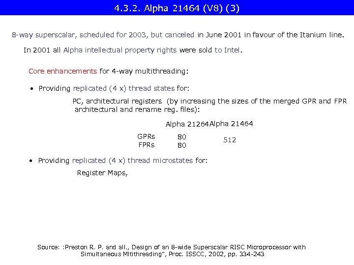 4. 3. 2. Alpha 21464 (V 8) (3) 8 -way superscalar, scheduled for 2003, but canceled in June 2001 in favour of the Itanium line. In 2001 all Alpha intellectual property rights were sold to Intel. Core enhancements for 4 -way multithreading: • Providing replicated (4 x) thread states for: PC, architectural registers (by increasing the sizes of the merged GPR and FPR architectural and rename reg. files): Alpha 21264 Alpha 21464 GPRs FPRs 80 80 512 • Providing replicated (4 x) thread microstates for: Register Maps, Source: : Preston R. P. and all. , Design of an 8 -wide Superscalar RISC Microprocessor with Simultaneous Mltithreading”, Proc. ISSCC, 2002, pp. 334 -243
 4. 3. 2. Alpha 21464 (V 8) (4) Figure 4. 3. 4: SMT pipeline in the Alpha 21464 (V 8) Source: Mukkherjee S. , „The Alpha 21364 and 21464 Microprocessors, ” http: //www. compaq. com
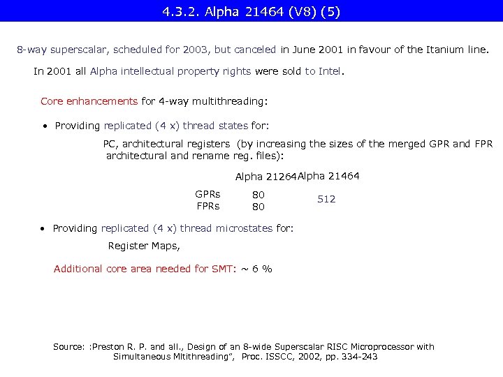 4. 3. 2. Alpha 21464 (V 8) (5) 8 -way superscalar, scheduled for 2003, but canceled in June 2001 in favour of the Itanium line. In 2001 all Alpha intellectual property rights were sold to Intel. Core enhancements for 4 -way multithreading: • Providing replicated (4 x) thread states for: PC, architectural registers (by increasing the sizes of the merged GPR and FPR architectural and rename reg. files): Alpha 21264 Alpha 21464 GPRs FPRs 80 80 512 • Providing replicated (4 x) thread microstates for: Register Maps, Additional core area needed for SMT: ~ 6 % Source: : Preston R. P. and all. , Design of an 8 -wide Superscalar RISC Microprocessor with Simultaneous Mltithreading”, Proc. ISSCC, 2002, pp. 334 -243
 4. 3. 3. IBM POWER 5 (1) POWER 5 enhancements vs the POWER 4: • on-chip memory control,
 4. 3. 3. IBM POWER 5 (2) Fabric Controller Figure 4. 3. 5: POWER 4 and POWER 5 system structures Source: R. Kalla, B. Sinharoy, J. M. Tendler: IBM Power 5 chip: A Dual-core multithreaded Processor, IEEE. Micro, Vol. 24, No. 2, March-April 2004, pp. 40 -47.
 4. 3. 3. IBM POWER 5 (3) POWER 5 enhancements vs the POWER 4: • on-chip memory control, • separate L 3/memory attachment,
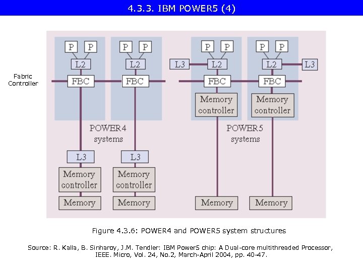 4. 3. 3. IBM POWER 5 (4) Fabric Controller Figure 4. 3. 6: POWER 4 and POWER 5 system structures Source: R. Kalla, B. Sinharoy, J. M. Tendler: IBM Power 5 chip: A Dual-core multithreaded Processor, IEEE. Micro, Vol. 24, No. 2, March-April 2004, pp. 40 -47.
 4. 3. 3. IBM POWER 5 (5) POWER 5 enhancements vs the POWER 4: • on-chip memory control, • separate L 3/memory attachment, • dual threaded.
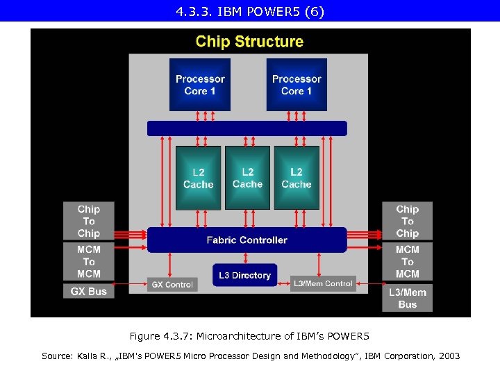 4. 3. 3. IBM POWER 5 (6) Figure 4. 3. 7: Microarchitecture of IBM’s POWER 5 Source: Kalla R. , „IBM's POWER 5 Micro Processor Design and Methodology”, IBM Corporation, 2003
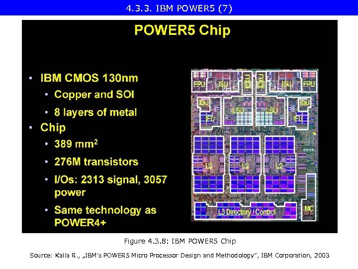 4. 3. 3. IBM POWER 5 (7) Figure 4. 3. 8: IBM POWER 5 Chip Source: Kalla R. , „IBM's POWER 5 Micro Processor Design and Methodology”, IBM Corporation, 2003
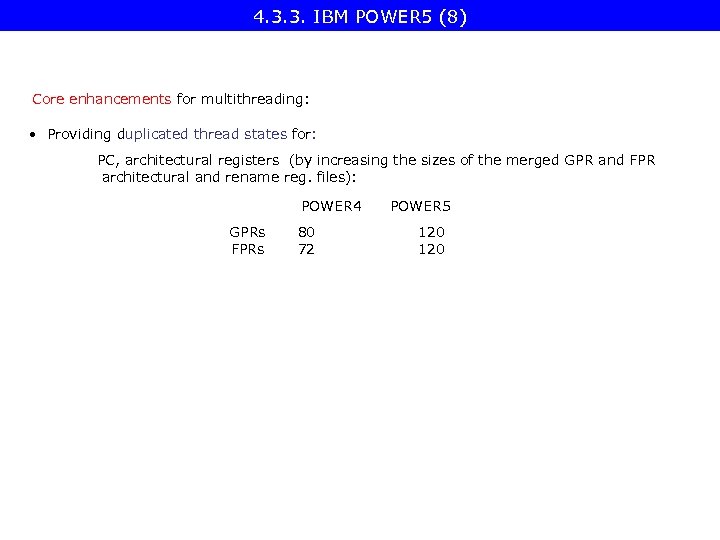 4. 3. 3. IBM POWER 5 (8) Core enhancements for multithreading: • Providing duplicated thread states for: PC, architectural registers (by increasing the sizes of the merged GPR and FPR architectural and rename reg. files): POWER 4 GPRs FPRs 80 72 POWER 5 120
 4. 3. 3. IBM POWER 5 (9) Figure 4. 3. 9: SMT pipeline of IBM’s POWER 5 Source: Kalla R. , „IBM's POWER 5 Micro Processor Design and Methodology”, IBM Corporation, 2003
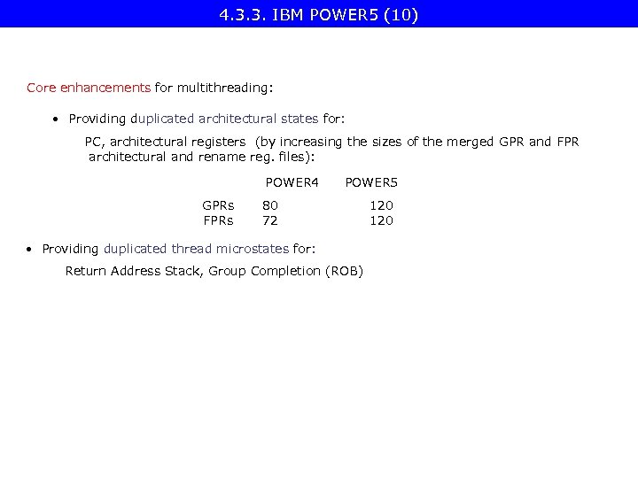 4. 3. 3. IBM POWER 5 (10) Core enhancements for multithreading: • Providing duplicated architectural states for: PC, architectural registers (by increasing the sizes of the merged GPR and FPR architectural and rename reg. files): POWER 4 GPRs FPRs POWER 5 80 72 • Providing duplicated thread microstates for: Return Address Stack, Group Completion (ROB) 120
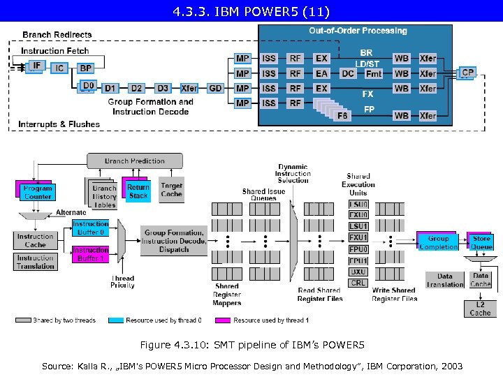 4. 3. 3. IBM POWER 5 (11) Figure 4. 3. 10: SMT pipeline of IBM’s POWER 5 Source: Kalla R. , „IBM's POWER 5 Micro Processor Design and Methodology”, IBM Corporation, 2003
 4. 3. 3. IBM POWER 5 (12) Core enhancements for multithreading: • Providing duplicated thread states for: PC, architectural registers (by increasing the sizes of the merged GPR and FPR architectural and rename reg. files): POWER 4 GPRs FPRs POWER 5 80 72 120 • Providing duplicated thread microstates for: Return Address Stack, Group Completion (ROB) • Providing increased (in fact duplicated) sizes for scarce or sensitive resorces, such as: Instruction Buffer, Store Queue
 4. 3. 3. IBM POWER 5 (13) Figure 4. 3. 11: SMT pipeline of IBM’s POWER 5 Source: Kalla R. , „IBM's POWER 5 Micro Processor Design and Methodology”, IBM Corporation, 2003
 4. 3. 3. IBM POWER 5 (14) Core enhancements for multithreading: • Providing duplicated thread states for: PC, architectural registers (by increasing the sizes of the merged GPR and FPR architectural and rename reg. files): POWER 4 GPRs FPRs POWER 5 80 72 120 • Providing duplicated thread microstates for: Return Address Stack, Group Completion (ROB) • Providing increased (duplicated) size for scarce or sensitive resorces, such as: Instruction Buffer, Store Queue Additional core area needed for SMT: ~ 10 %
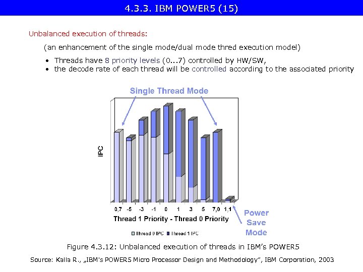 4. 3. 3. IBM POWER 5 (15) Unbalanced execution of threads: (an enhancement of the single mode/dual mode thred execution model) • Threads have 8 priority levels (0. . . 7) controlled by HW/SW, • the decode rate of each thread will be controlled according to the associated priority Figure 4. 3. 12: Unbalanced execution of threads in IBM’s POWER 5 Source: Kalla R. , „IBM's POWER 5 Micro Processor Design and Methodology”, IBM Corporation, 2003
 4. 3. 3. IBM POWER 5 (16) Development effort: • Concept phase: • High level design phase: • Implementation phase: ~ 10 persons/ 4 month ~ 50 persons/ 6 month ~ 200 persons/ 12 -18 month Source: Kalla R. , „IBM's POWER 5 Micro Processor Design and Methodology”, IBM Corporation, 2003


