

29dcbf676480fb2eec2aa9edbd578280.ppt
- Количество слайдов: 8
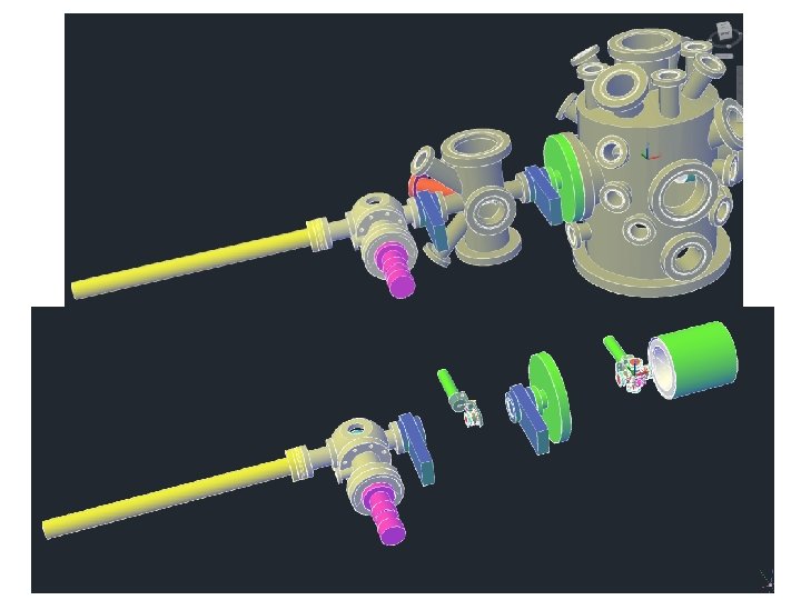
 MSD XPS/UPS plus LEED optics (the current refined scheme for SEY measurements used by Slade Jokela Planned q Addition of the second (smaller) load-lock chamber (work in progress) so that the existing larger chamber can be populated with more diagnostics q The 2 nd chamber will be equipped with o one electron gun and one ion gun o quadrupole MS o a new RGA - for now (to buy), later can be used on the main chamber of the XPS/UPS apparatus o high resolution / efficiency VG (resurrected) MS analyzer – in the future
 MSD Planned experiments on aging of MCPs § irradiation of flat ALD-functionalized MCP materials with electron beam in the larger load-lock chamber (controlled fluences and controlled electron impact energy) § measuring mass spectra of electron stimulated desorption § heating these samples in the larger load-lock chamber (halogen lamp) § measuring mass spectra of thermal desorption § moving samples into XPS/UPS main chamber to check § surface composition with XPS § SEY § moving samples back into larger load-lock chamber to get more electron fluences No way to look at changes in surface morphology and to probe small spots. Go to CNM for this.
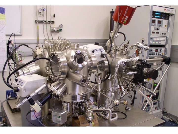
 CNM Variable-temperature, ultra-high-vacuum, atomic force microscope/scanning tunneling microscope Omicron VT-AFM XA (N. Guisinger, Electronic & Magnetic Materials & Devices Group) Measurement modes include: Contact and non-contact AFM Magnetic force microscopy (MFM) Scanning tunneling spectroscopy Preparation tools include: Resistive sample heating Direct current heating E-beam heating Sputter ion etching Gas dosing E-beam evaporation An analysis chamber contains combined four-grid LEED/Auger optics Heavily booked instrument
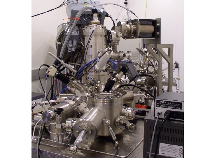
 CNM Scanning probe/scanning electron microscopy: Omicron UHV Nanoprobe (N. Guisinger, Electronic & Magnetic Materials & Devices Group) Local, nondestructive four-point contact measurements and function testing of nanodevices within complex structures; accurate probe positioning and safe approach of fragile probe tips having diameters in the range of a few tens of nanometers or less. Four independent STM probe tips with simultaneous SEM imaging enables a large field of view for coarse positioning as well as fine positioning of nanometer-sized structures with the SEM's high-resolution capabilities. UHV Gemini column for chemical mapping by scanning auger microscopy and magnetic imaging by SEM with polarization analysis (SEMPA). This yields complementary information on sample conductance, topography, chemistry, and magnetism. An instrument with just a few users – available for most of the time
 • Omicron UHV Nanoprobe – Nanoprobes for device testing • Scanning Tunneling Microscope – Scanning Electron Microscopy – Low Energy Electron Diffraction (LEED) – UHV Gemini Column • Auger Electron Spectroscopy (Chemical Mapping) • Magnetic Imaging by SEM polarization analysis (SEMPA) – Sample preparation • Resistive Sample Heating