7de21f0e03131c82b80bed0c8792b33d.ppt
- Количество слайдов: 44
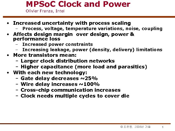 MPSo. C Clock and Power Olivier Franza, Intel • Increased uncertainty with process scaling – Process, voltage, temperature variations, noise, coupling • Affects design margin over design, power & performance loss – Increased power constraints – Increasing leakage, power (density, delivery) limitations • More transistors mean: – Larger clock distribution networks – Higher capacitance (more load and parasitics) • With each new technology: – Gate delay decreases ~25% – Wire delay increases ~100% – Cross-chip communication increases – Clock needs multiple cycles to cover die © 조준동, 2006년 가을 1
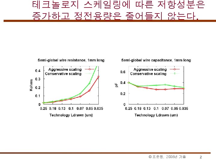 테크놀로지 스케일링에 따른 저항성분은 증가하고 정전용량은 줄어들지 않는다. © 조준동, 2006년 가을 2
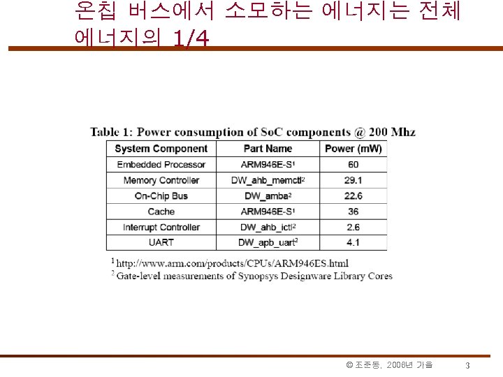 온칩 버스에서 소모하는 에너지는 전체 에너지의 1/4 © 조준동, 2006년 가을 3
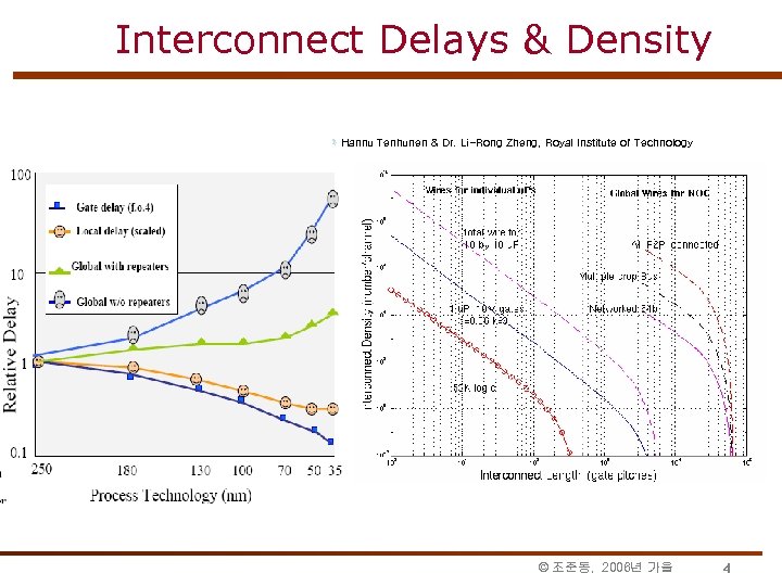 Interconnect Delays & Density ëHannu Tenhunen & Dr. Li-Rong Zheng, Royal Institute of Technology © 조준동, 2006년 가을 4
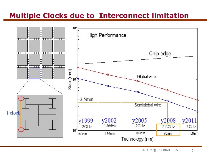 Multiple Clocks due to Interconnect limitation © 조준동, 2006년 가을 5
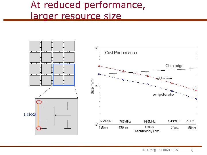 At reduced performance, larger resource size © 조준동, 2006년 가을 6
 Multiple clock domains • Low skew and jitter ALWAYS a must • Clock modeling requires more accuracy • Within-die variations, inductance, crosstalk, electromigration, self-heat, … • Floor plan modularity • Think adding/removing cores seamlessly! • Hierarchical clock partitioning • Reduce global clock and possibly relax its requirements • Generate “locally”-used clock “locally” • Implement clock domain deskewing techniques • Bound clock problem into simple, reliable, efficient domains © 조준동, 2006년 가을 7
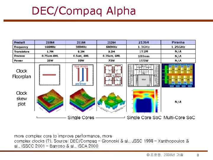 DEC/Compaq Alpha more complex core to improve performance, more complex clocks (? ), Source: DEC/Compaq – Gronoski & al. , JSSC 1998 – Xanthopoulos & al. , ISSCC 2001 – Barroso & al. , ISCA 2000 © 조준동, 2006년 가을 8
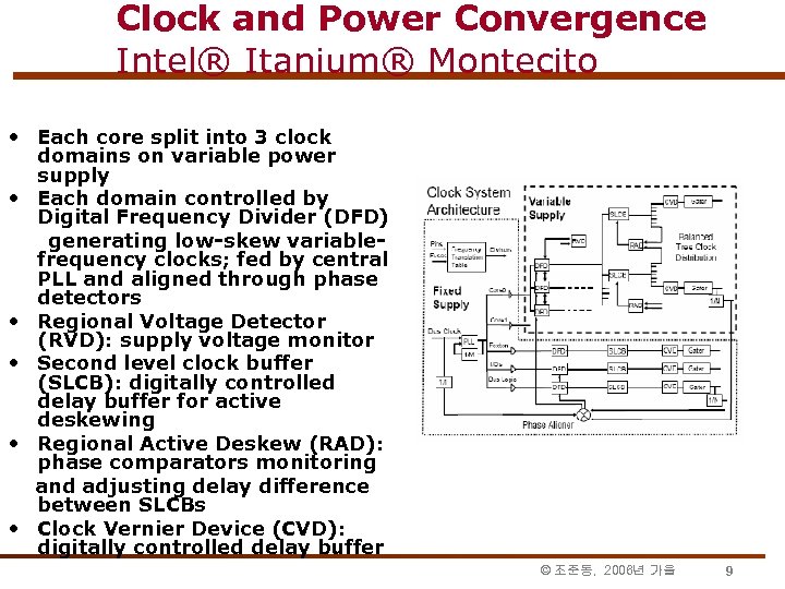 Clock and Power Convergence Intel® Itanium® Montecito • Each core split into 3 clock domains on variable power supply • Each domain controlled by Digital Frequency Divider (DFD) generating low-skew variablefrequency clocks; fed by central PLL and aligned through phase detectors • Regional Voltage Detector (RVD): supply voltage monitor • Second level clock buffer (SLCB): digitally controlled delay buffer for active deskewing • Regional Active Deskew (RAD): phase comparators monitoring and adjusting delay difference between SLCBs • Clock Vernier Device (CVD): digitally controlled delay buffer © 조준동, 2006년 가을 9
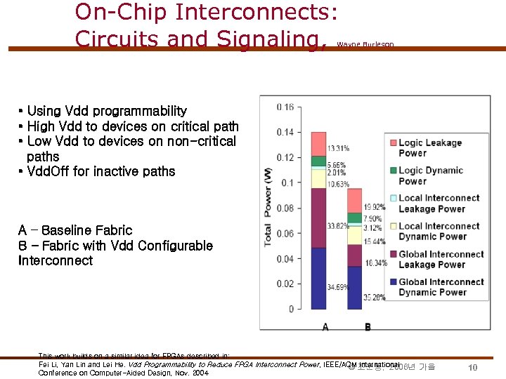 On-Chip Interconnects: Circuits and Signaling, Wayne Burleson • Using Vdd programmability • High Vdd to devices on critical path • Low Vdd to devices on non-critical paths • Vdd. Off for inactive paths A – Baseline Fabric B – Fabric with Vdd Configurable Interconnect This work builds on a similar idea for FPGAs described in: Fei Li, Yan Lin and Lei He. Vdd Programmability to Reduce FPGA Interconnect Power, IEEE/ACM International © 조준동, 2006년 가을 Conference on Computer-Aided Design, Nov. 2004 10
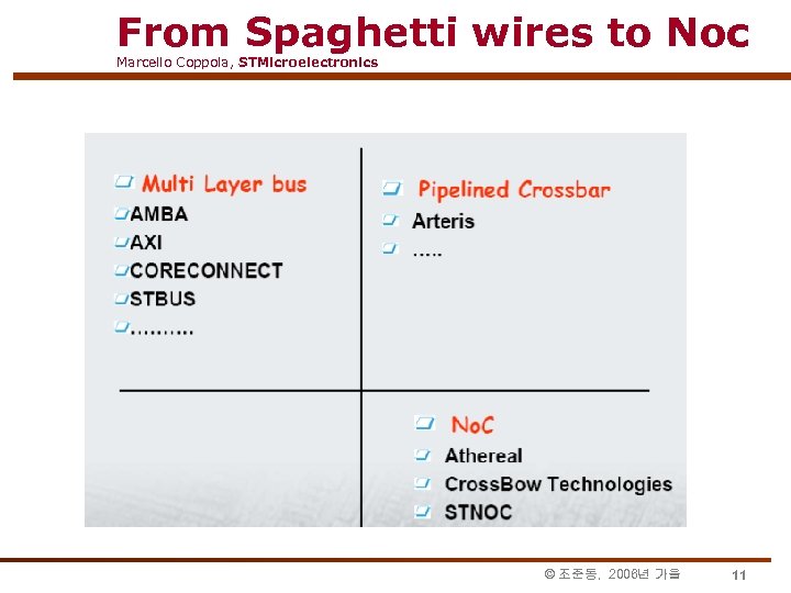 From Spaghetti wires to Noc Marcello Coppola, STMicroelectronics © 조준동, 2006년 가을 11
 Benchmarks, EE Times, 7/2005 • Xpipes, Bologna and Stanford : compared w/ Amba AHB multilayer bus, 21% faster, but worse latency • When, Univ. of Kaiserslautern: LPDC decoder: 500 Mhz vs 64 Mhz (fixed bus), but 30 W vs. 700 m. W, twice the die size. • Arteris: better die size, comparable power consumption, 740 Mhz (250 Mhz) • Sonics. MX: power-efficient mobile-handset w/ power management • STNo. C, Spidergon: topology w/ degree 2 -3 © 조준동, 2006년 가을 12
 No. C Applications http: //www. eit. uni-kl. de/wehn • Turbo-Decoder UMTS compliant, 100 Mbit: large flexibilty w/ 14 parallel units, area = 16. 84 mm 2 (14 mm 2 PUs, 2. 8 mm 2 No. C) • LDPC Decoding, T. Theocharides, G. Link, N. Chip, T. Theocharides, G. Link, N. Vijaykrishnan, M. J. Irwin, Int. Conference on VLSI Design 2005 – 1024 Bit block size, 1. 2 Gb/s, R=0. 75 – No. C: 5 x 5 2 D mesh, dimension-order routing, large flexibility – 160 nm CMOS Technology, 1. 8 V, 500 MHz, 110 mm 2, ~30 Watt © 조준동, 2006년 가을 13
 Reliable design, G. De Micheli 1. Manufacturing imperfections: More likely to happen as lithography scales down 2. Approximations during design: Uncertainty about details of design 3. Aging: Oxide breakdown, electromigration 4. Environment-induced Soft-errors (Data corruption due external radiation exposure), electro-magnetic interference 5. Operating-mode induced: Extremely-low voltage supply © 조준동, 2006년 가을 14
 Dealing with variability • Most variability problems that induce timing errors 1. 2. 3. 4. Power supply variation Wire length estimation Crosstalk Soft errors © 조준동, 2006년 가을 15
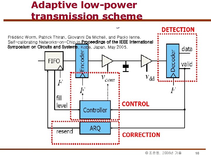 Adaptive low-power transmission scheme Frédéric Worm, Patrick Thiran, Giovanni De Micheli, and Paolo Ienne. Self-calibrating Networks-on-Chip. In Proceedings of the IEEE International Symposium on Circuits and Systems, Kobe, Japan, May 2005. © 조준동, 2006년 가을 16
 Reduced Energy Consumption © 조준동, 2006년 가을 17
 Low-Power Network-on-Chip for High-Performance So. C Design Lee, K. ; Lee, S. -J. ; Yoo, H. -J. Very Large Scale Integration (VLSI) Systems, IEEE Transactions on Volume 14, Issue 2, Feb. 2006 Page(s): 148 - 160 Digital Object Identifier 10. 1109/TVLSI. 2005. 863753 Se-Joong Lee; Kangmin Lee; Seong-Jun Song; Hoi-Jun Yoo Circuits and Systems II: Express Briefs, IEEE Transactions on [see also Circuits and Systems II: Analog and Digital Signal Processing, IEEE Transactions on] Volume 52, Issue 6, June 2005 Page(s): 308 - 312 Digital Object Identifier 10. 1109/TCSII. 2005. 848972 성균관대학교 정보통신공학부 © 조준동 2006년 여름 18
 Contents • Introduction • No. C Architecture – Overall Architecture – Packet Routing Scheme – Chip-to-Chip Connectivity – Topology Selection – Physical Transfer Unit Size – Hierarchical Circuit/Packet Switching – Synchronization – No. C Protocol • Low-Power Techniques – Low-Swing Signal – Mux-Tree Based Round-Robin Scheduler – Crossbar Partial Activation Technique – Low-Energy Coding On-Chip Serial Link • Implementation and Measurement Result • Conclusion © 조준동, 2006년 가을 19
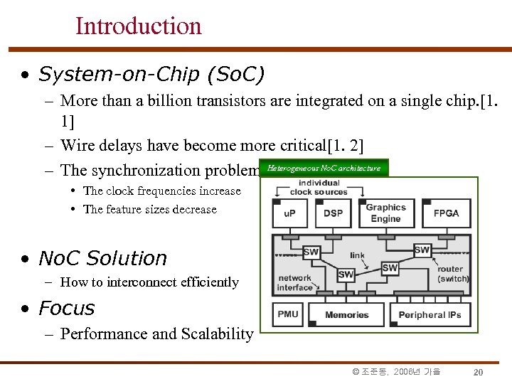 Introduction • System-on-Chip (So. C) – More than a billion transistors are integrated on a single chip. [1. 1] – Wire delays have become more critical[1. 2] – The synchronization problem Heterogeneous No. C architecture • The clock frequencies increase • The feature sizes decrease • No. C Solution – How to interconnect efficiently • Focus – Performance and Scalability © 조준동, 2006년 가을 20
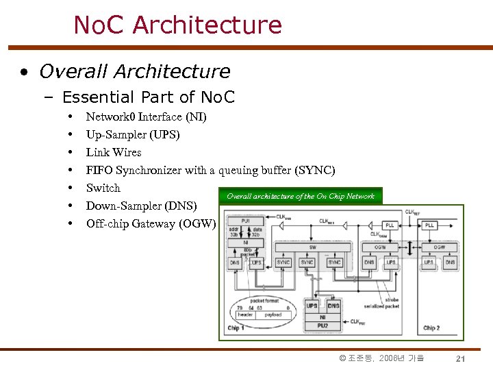 No. C Architecture • Overall Architecture – Essential Part of No. C • • Network 0 Interface (NI) Up-Sampler (UPS) Link Wires FIFO Synchronizer with a queuing buffer (SYNC) Switch Overall architecture of the On Chip Network Down-Sampler (DNS) Off-chip Gateway (OGW) © 조준동, 2006년 가을 21
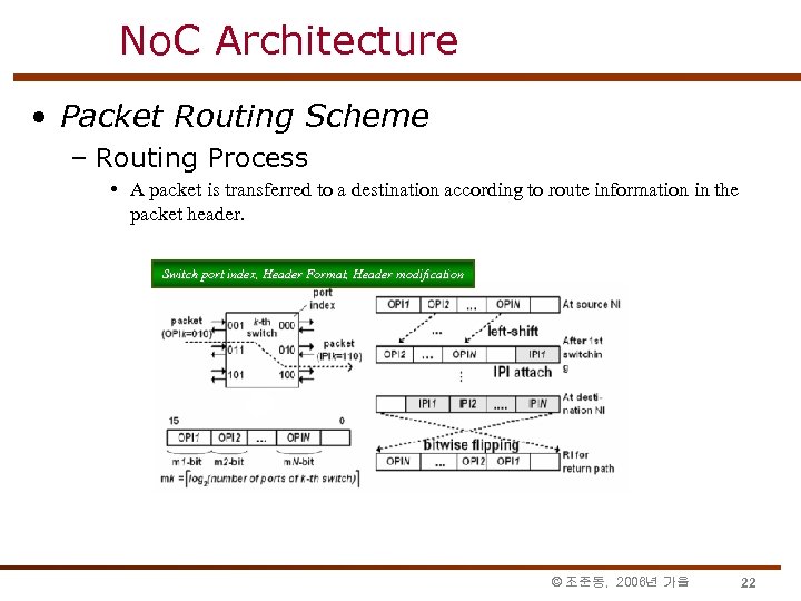 No. C Architecture • Packet Routing Scheme – Routing Process • A packet is transferred to a destination according to route information in the packet header. Switch port index, Header Format, Header modification © 조준동, 2006년 가을 22
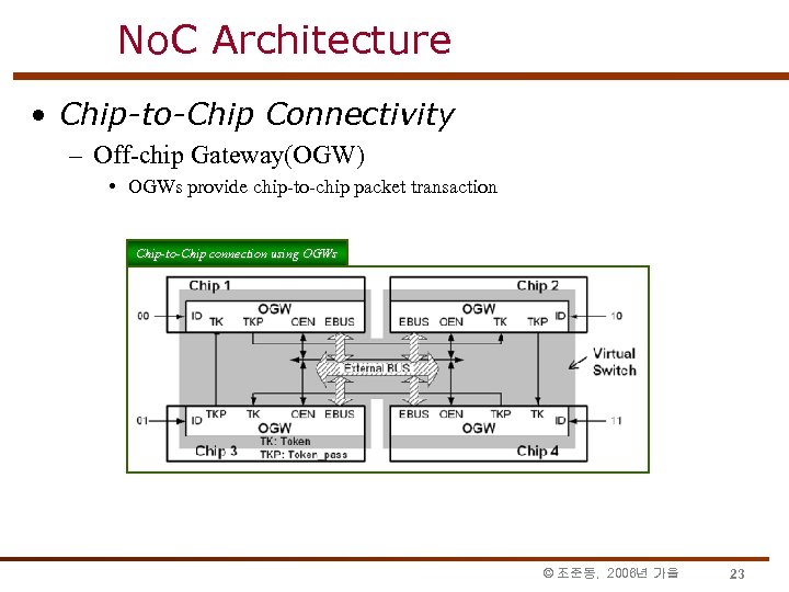 No. C Architecture • Chip-to-Chip Connectivity – Off-chip Gateway(OGW) • OGWs provide chip-to-chip packet transaction Chip-to-Chip connection using OGWs © 조준동, 2006년 가을 23
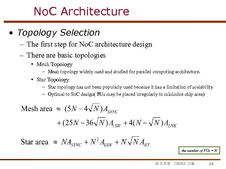 No. C Architecture • Topology Selection – The first step for No. C architecture design – There are basic topologies • Mesh Topology – Mesh topology widely used and studied for parallel computing architecture. • Star Topology – Star topology has not been popularly used because it has a limitation of scalability – Optimal to So. C design( PUs may be placed irregularly to minimize chip area) the number of PUs = N © 조준동, 2006년 가을 24
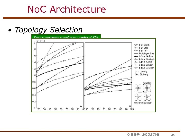 No. C Architecture • Topology Selection Energy consumption according to a number of PUs © 조준동, 2006년 가을 25
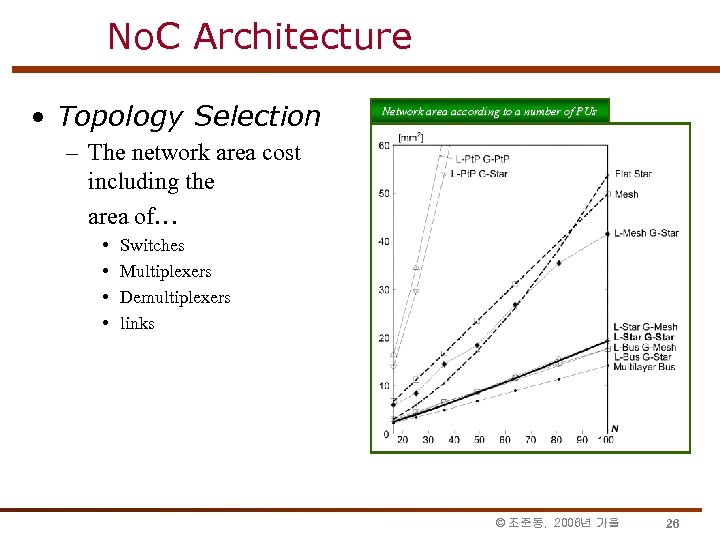 No. C Architecture • Topology Selection Network area according to a number of PUs – The network area cost including the area of… • • Switches Multiplexers Demultiplexers links © 조준동, 2006년 가을 26
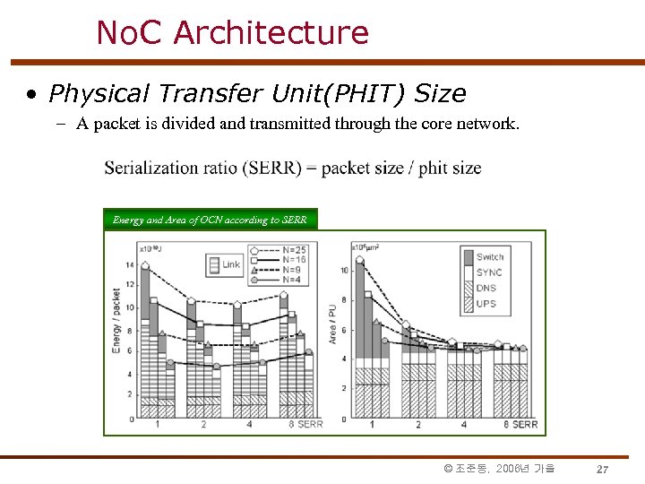 No. C Architecture • Physical Transfer Unit(PHIT) Size – A packet is divided and transmitted through the core network. Energy and Area of OCN according to SERR © 조준동, 2006년 가을 27
 No. C Architecture • Hierarchical Circuit and Packet Switching – Local Intracluster Network → Circuit Switching • The Circuit switching does not need packet buffers • Area and Power consumption can be reduced – Global Intercluster Network → Packet Switching • The global intercluster traffic shares the bandwidth of the switch-to-switch link • The throughput of the shared and limited link is more important rather than the latency © 조준동, 2006년 가을 28
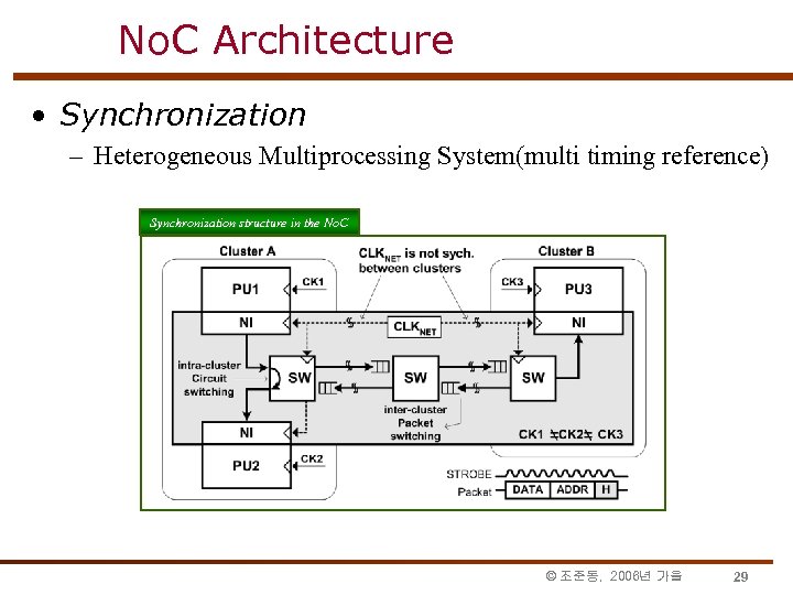 No. C Architecture • Synchronization – Heterogeneous Multiprocessing System(multi timing reference) Synchronization structure in the No. C © 조준동, 2006년 가을 29
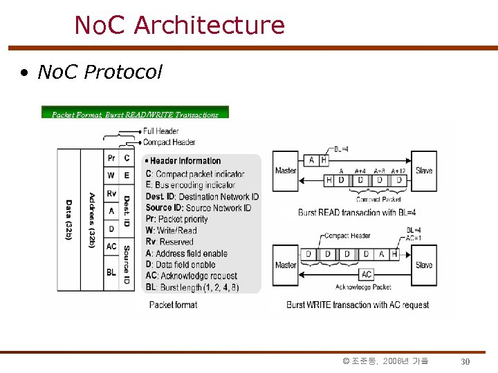 No. C Architecture • No. C Protocol Packet Format, Burst READ/WRITE Transactions © 조준동, 2006년 가을 30
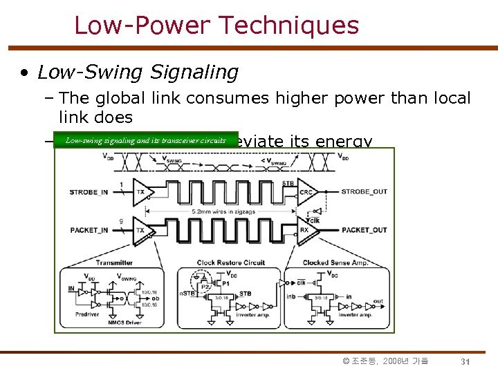 Low-Power Techniques • Low-Swing Signaling – The global link consumes higher power than local link does Low-swing signaling and its transceiver circuits – Low-signaling can alleviate its energy consumption significantly[2. 13] © 조준동, 2006년 가을 31
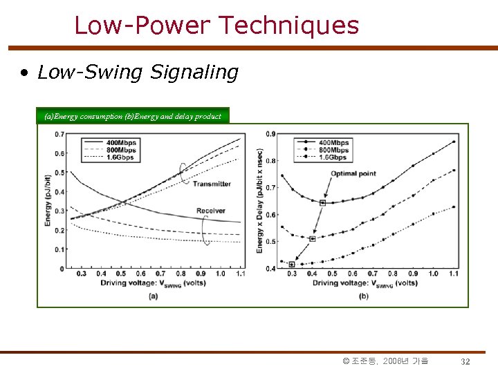 Low-Power Techniques • Low-Swing Signaling (a)Energy consumption (b)Energy and delay product (b)Energy © 조준동, 2006년 가을 32
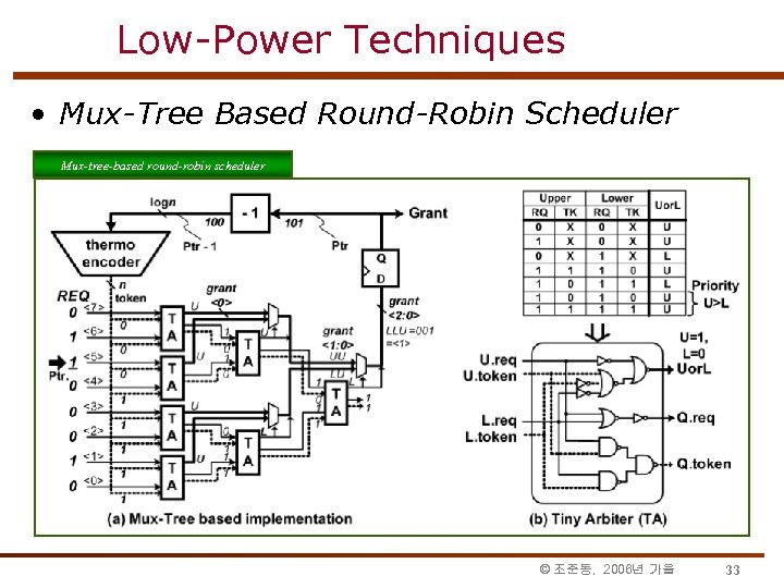 Low-Power Techniques • Mux-Tree Based Round-Robin Scheduler Mux-tree-based round-robin scheduler Mux-tree-based © 조준동, 2006년 가을 33
![Low-Power Techniques • Crossbar Partial Activation Techniques (CPAT)[2. 10] Schematic Diagram of Crossbar © Low-Power Techniques • Crossbar Partial Activation Techniques (CPAT)[2. 10] Schematic Diagram of Crossbar ©](https://present5.com/presentation/7de21f0e03131c82b80bed0c8792b33d/image-34.jpg) Low-Power Techniques • Crossbar Partial Activation Techniques (CPAT)[2. 10] Schematic Diagram of Crossbar © 조준동, 2006년 가을 34
Low-Power Techniques • Crossbar Partial Activation Techniques (CPAT)[2. 10] Schematic Diagram of Crossbar © 조준동, 2006년 가을 34
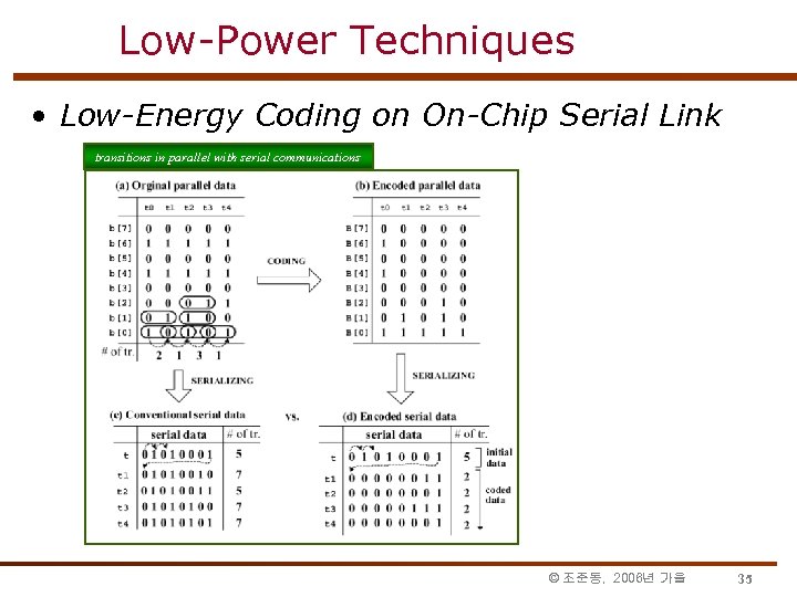 Low-Power Techniques • Low-Energy Coding on On-Chip Serial Link transitions in parallel with serial communications © 조준동, 2006년 가을 35
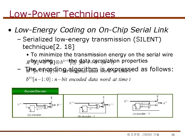 Low-Power Techniques • Low-Energy Coding on On-Chip Serial Link – Serialized low-energy transmission (SILENT) technique[2. 18] • To minimize the transmission energy on the serial wire by using the data correlation properties – The encoding algorithm is expressed as follows: Encoder/Decoder © 조준동, 2006년 가을 36
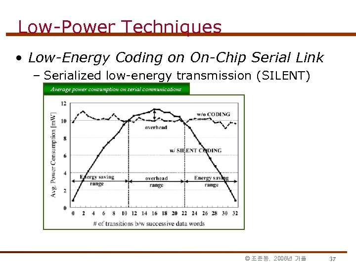 Low-Power Techniques • Low-Energy Coding on On-Chip Serial Link – Serialized low-energy transmission (SILENT) Average power consumption 18] technique[2. on serial communications © 조준동, 2006년 가을 37
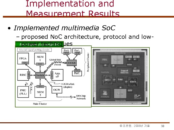 Implementation and Measurement Results • Implemented multimedia So. C – proposed No. C architecture, protocol and low. Block diagram of a prototype So. C power techniques © 조준동, 2006년 가을 38
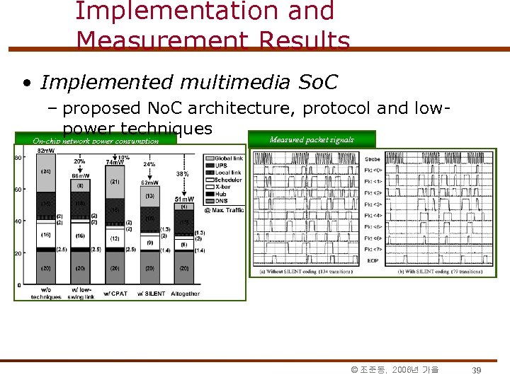 Implementation and Measurement Results • Implemented multimedia So. C – proposed No. C architecture, protocol and lowpower techniques Measured packet signals On-chip network power consumption © 조준동, 2006년 가을 39
 Conclusion • A low-power No. C is designed and implemented for high-performance So. C application • Heterogeneous IPs are interconnected in a hierarchical star topology • Various power-efficient techniques were suggested and implemented © 조준동, 2006년 가을 40
![Reference • • • [1. 1] R. Woo et al. , “A 210 m. Reference • • • [1. 1] R. Woo et al. , “A 210 m.](https://present5.com/presentation/7de21f0e03131c82b80bed0c8792b33d/image-41.jpg) Reference • • • [1. 1] R. Woo et al. , “A 210 m. W graphics LSI implementing full 3 D pipeline with 264 Mtexels/s texturing for mobile multimedia applications, ” in ISSCC Tech. Dig. , 2003, pp. 44 – 45. [1. 2] AMBA™ AXI Protocol Specification (2003). [Online]. Available: http: //www. arm. com [1. 3] M. Sgroi et al. , “Addressing the system-on-a-chip interconnection woes through communication-based design, ”in Proc. Design Automation Conf. , 2001, pp. 667– 672. [1. 4] L. Benini et al. , “Powering networks on chips, ” in Proc. Int. Symp. System Synthesis, 2001, pp. 33– 38. [1. 5] P. Guerrier et al. , “A generic architecture for on-chip packet-switched interconnections, ” in Proc. Design Automation Test Eur. Conf. Exhib. , 2000, pp. 250– 256. [1. 6] S. Kumar et al. , “A network on chip architecture and design methodology, ”in Proc. Ann Symp. VLSI, 2002, pp. 117– 124. [1. 7] W. J. Dally et al. , “Route packets, not wires: On-chip interconnection networks, ” in Proc. f Design Automation Conf. , 2001, pp. 684– 689. [1. 8] H. Zhang et al. , “A 1 -V heterogeneous reconfigurable DSP IC for wireless baseband digital signal processing, ” J. Solid-State Circuits, vol. 35, no. 11, pp. 1697– 2000, Nov. 2000. [1. 9] M. Taylor et al. , “A 16 -issue multiple-program-counter microprocessor with point-topoint scalar operand network, ” in ISSCC Tech. Dig. , 2003, pp. 170– 171. [1. 10] S. Lee et al. , “An 800 MHz star-connected on-chip network for application to systems on a chip, ” in ISSCC Tech. Dig. , 2003, pp. 468– 469. © 조준동, 2006년 가을 41
Reference • • • [1. 1] R. Woo et al. , “A 210 m. W graphics LSI implementing full 3 D pipeline with 264 Mtexels/s texturing for mobile multimedia applications, ” in ISSCC Tech. Dig. , 2003, pp. 44 – 45. [1. 2] AMBA™ AXI Protocol Specification (2003). [Online]. Available: http: //www. arm. com [1. 3] M. Sgroi et al. , “Addressing the system-on-a-chip interconnection woes through communication-based design, ”in Proc. Design Automation Conf. , 2001, pp. 667– 672. [1. 4] L. Benini et al. , “Powering networks on chips, ” in Proc. Int. Symp. System Synthesis, 2001, pp. 33– 38. [1. 5] P. Guerrier et al. , “A generic architecture for on-chip packet-switched interconnections, ” in Proc. Design Automation Test Eur. Conf. Exhib. , 2000, pp. 250– 256. [1. 6] S. Kumar et al. , “A network on chip architecture and design methodology, ”in Proc. Ann Symp. VLSI, 2002, pp. 117– 124. [1. 7] W. J. Dally et al. , “Route packets, not wires: On-chip interconnection networks, ” in Proc. f Design Automation Conf. , 2001, pp. 684– 689. [1. 8] H. Zhang et al. , “A 1 -V heterogeneous reconfigurable DSP IC for wireless baseband digital signal processing, ” J. Solid-State Circuits, vol. 35, no. 11, pp. 1697– 2000, Nov. 2000. [1. 9] M. Taylor et al. , “A 16 -issue multiple-program-counter microprocessor with point-topoint scalar operand network, ” in ISSCC Tech. Dig. , 2003, pp. 170– 171. [1. 10] S. Lee et al. , “An 800 MHz star-connected on-chip network for application to systems on a chip, ” in ISSCC Tech. Dig. , 2003, pp. 468– 469. © 조준동, 2006년 가을 41
![Reference • • • [1. 11] K. Lee et al. , “A 51 m. Reference • • • [1. 11] K. Lee et al. , “A 51 m.](https://present5.com/presentation/7de21f0e03131c82b80bed0c8792b33d/image-42.jpg) Reference • • • [1. 11] K. Lee et al. , “A 51 m. W 1. 6 GHz on-chip network for low power heterogeneous So. C platform, ” in ISSCC Tech. Dig. , 2004, pp. 152– 153. [1. 12] A. Laffely et al. , “Adaptive system on a chip (ASOC): A backbone for power-aware signal processing cores, ” in Proc. IEEE Int. Conf. Image Processing, Barcelona, Spain, Sep. 2003. [1. 13] E. Rijpkema et al. , “Tradeoffs in the design of a router with both guaranteed and best-effort services for networks on chip, ” in Proc. Design Automation Test in Eur. , Mar. 2003, pp. 350– 355. [1. 14] D. Bertozzi et al. , “Xpipes: Anetwork-on-chip architecture for gigascale system-onchip, ” IEEE Circuits Syst. Mag. , vol. 4, no. 2, pp. 18– 31, Feb. 2004. [1. 15] S. Kimura et al. , “An on-chip high speed serial communication method based on independent ring oscillators, ” in ISSCC Tech. Dig. , 2003, pp. 390– 391. [1. 16] H. J. Siegel et al. , Interconnection Networks for Large-Scale Parallel Processing: Theory and Case Studies. New York: Mc. Graw-Hill, 1990. [1. 17] K. Lee et al. , “SILENT: Serialized low energy transmission coding for on-chip interconnection networks, ” in Proc. Int. Conf. Computer-Aided Design, 2004, pp. 448– 451. [1. 18] W. J. Dally et al. , Digital Systems Engineering. Cambridge, U. K. : Cambridge Univ. Press, 1998, ch. 10. [1. 19] M. Cooperman et al. , “CMOS gigabit-per-second switching, ” J. Solid- State Circuits, vol. 28, no. 6, pp. 631– 639, Jun. 1993. [1. 20] T. T. Ye et al. , “Analysis of power consumption on switch fabrics in network routers, ” in Proc. Design Automation Conf. , 2002, pp. 524– 529. [1. 21] K. Lee et al. , “A distributed on-chip crossbar switch scheduler for on-chip networks, ” in Proc. Custom Integrated Circuits Conf. , May 2003, pp. 671– 674. © 조준동, 2006년 가을 42
Reference • • • [1. 11] K. Lee et al. , “A 51 m. W 1. 6 GHz on-chip network for low power heterogeneous So. C platform, ” in ISSCC Tech. Dig. , 2004, pp. 152– 153. [1. 12] A. Laffely et al. , “Adaptive system on a chip (ASOC): A backbone for power-aware signal processing cores, ” in Proc. IEEE Int. Conf. Image Processing, Barcelona, Spain, Sep. 2003. [1. 13] E. Rijpkema et al. , “Tradeoffs in the design of a router with both guaranteed and best-effort services for networks on chip, ” in Proc. Design Automation Test in Eur. , Mar. 2003, pp. 350– 355. [1. 14] D. Bertozzi et al. , “Xpipes: Anetwork-on-chip architecture for gigascale system-onchip, ” IEEE Circuits Syst. Mag. , vol. 4, no. 2, pp. 18– 31, Feb. 2004. [1. 15] S. Kimura et al. , “An on-chip high speed serial communication method based on independent ring oscillators, ” in ISSCC Tech. Dig. , 2003, pp. 390– 391. [1. 16] H. J. Siegel et al. , Interconnection Networks for Large-Scale Parallel Processing: Theory and Case Studies. New York: Mc. Graw-Hill, 1990. [1. 17] K. Lee et al. , “SILENT: Serialized low energy transmission coding for on-chip interconnection networks, ” in Proc. Int. Conf. Computer-Aided Design, 2004, pp. 448– 451. [1. 18] W. J. Dally et al. , Digital Systems Engineering. Cambridge, U. K. : Cambridge Univ. Press, 1998, ch. 10. [1. 19] M. Cooperman et al. , “CMOS gigabit-per-second switching, ” J. Solid- State Circuits, vol. 28, no. 6, pp. 631– 639, Jun. 1993. [1. 20] T. T. Ye et al. , “Analysis of power consumption on switch fabrics in network routers, ” in Proc. Design Automation Conf. , 2002, pp. 524– 529. [1. 21] K. Lee et al. , “A distributed on-chip crossbar switch scheduler for on-chip networks, ” in Proc. Custom Integrated Circuits Conf. , May 2003, pp. 671– 674. © 조준동, 2006년 가을 42
![Reference • • • [2. 1] International Technology Roadmap for Semiconductors [Online]. Available: http: Reference • • • [2. 1] International Technology Roadmap for Semiconductors [Online]. Available: http:](https://present5.com/presentation/7de21f0e03131c82b80bed0c8792b33d/image-43.jpg) Reference • • • [2. 1] International Technology Roadmap for Semiconductors [Online]. Available: http: //public. itrs. net [2. 2] W. Dally et al. , “Route packets, not wires: On-chip interconnection networks, ”in Proc. Des. Autom. Conf. , Jun. 2001, pp. 684– 689. [2. 3] L. Benini et al. , “Networks on chips: A new So. C paradigm, ” IEEE Computer, vol. 36, no. 1, pp. 70– 78, Jan. 2002. [2. 4] D. Bertozzi et al. , “Xpipes: A network-on-chip architecture for gigascale system-onchip, ” IEEE Circuits Syst. Mag. , vol. 4, no. 2, pp. 18– 31, 2004. [2. 5] E. Rijpkema et al. , “Trade offs in the design of a router with both guaranteed and best-effort services for networks on chip, ” in Proc. Des. , Autom. Test Europe Conf. , Mar. 2003, pp. 350– 355. [2. 6] V. Nollet et al. , “Operating-system controlled network on chip, ” in Proc. Des. Autom. Conf. , Jun. 2004, pp. 256– 259. [2. 7] J. -S. Kim et al. , “On-chip network based embedded core testing, ” in Proc. IEEE Int. So. C Conf. , Sep. 2004, pp. 223– 226. [2. 8] S. -J. Lee et al. , “An 800 MHz star-connected on-chip network for application to systems on a chip, ” in IEEE Int. Solid-State Circuits Conf. Dig. Tech. Papers, Feb. 2003, pp. 468– 469. [2. 9] M. Taylor et al. , “A 16 -issue multiple-program-counter microprocessor with point-topoint scalar operand network, ” in IEEE Int. Solid-State Circuits Conf. Dig. Tech. Papers, Feb. 2003, pp. 170– 171. [2. 10] K. Lee et al. , “A 51 m. W 1. 6 GHz on-chip network for low-power heterogeneous So. C platform, ” in IEEE Int. Solid-State Circuits Conf. Dig. Tech. Papers, Feb. 2004, pp. 152– 153. [2. 11] H. Wang et al. , “A technology-aware and energy-oriented topology exploration for on-chip networks, ” in Proc. Des. , Autom. Test Europe Conf. , Mar. 2005, pp. 1238– 1243. [2. 12] BONE: Network-on-Chip Protocol [Online]. Available: http: //ssl. kaist. ac. kr/ocn © 조준동, 2006년 가을 43
Reference • • • [2. 1] International Technology Roadmap for Semiconductors [Online]. Available: http: //public. itrs. net [2. 2] W. Dally et al. , “Route packets, not wires: On-chip interconnection networks, ”in Proc. Des. Autom. Conf. , Jun. 2001, pp. 684– 689. [2. 3] L. Benini et al. , “Networks on chips: A new So. C paradigm, ” IEEE Computer, vol. 36, no. 1, pp. 70– 78, Jan. 2002. [2. 4] D. Bertozzi et al. , “Xpipes: A network-on-chip architecture for gigascale system-onchip, ” IEEE Circuits Syst. Mag. , vol. 4, no. 2, pp. 18– 31, 2004. [2. 5] E. Rijpkema et al. , “Trade offs in the design of a router with both guaranteed and best-effort services for networks on chip, ” in Proc. Des. , Autom. Test Europe Conf. , Mar. 2003, pp. 350– 355. [2. 6] V. Nollet et al. , “Operating-system controlled network on chip, ” in Proc. Des. Autom. Conf. , Jun. 2004, pp. 256– 259. [2. 7] J. -S. Kim et al. , “On-chip network based embedded core testing, ” in Proc. IEEE Int. So. C Conf. , Sep. 2004, pp. 223– 226. [2. 8] S. -J. Lee et al. , “An 800 MHz star-connected on-chip network for application to systems on a chip, ” in IEEE Int. Solid-State Circuits Conf. Dig. Tech. Papers, Feb. 2003, pp. 468– 469. [2. 9] M. Taylor et al. , “A 16 -issue multiple-program-counter microprocessor with point-topoint scalar operand network, ” in IEEE Int. Solid-State Circuits Conf. Dig. Tech. Papers, Feb. 2003, pp. 170– 171. [2. 10] K. Lee et al. , “A 51 m. W 1. 6 GHz on-chip network for low-power heterogeneous So. C platform, ” in IEEE Int. Solid-State Circuits Conf. Dig. Tech. Papers, Feb. 2004, pp. 152– 153. [2. 11] H. Wang et al. , “A technology-aware and energy-oriented topology exploration for on-chip networks, ” in Proc. Des. , Autom. Test Europe Conf. , Mar. 2005, pp. 1238– 1243. [2. 12] BONE: Network-on-Chip Protocol [Online]. Available: http: //ssl. kaist. ac. kr/ocn © 조준동, 2006년 가을 43
![Reference • • • [2. 13] R. Ho et al. , “Efficient on-chip global Reference • • • [2. 13] R. Ho et al. , “Efficient on-chip global](https://present5.com/presentation/7de21f0e03131c82b80bed0c8792b33d/image-44.jpg) Reference • • • [2. 13] R. Ho et al. , “Efficient on-chip global interconnects, ” in IEEE Symp. VLSI Circuits Dig. Tech. Papers, Jun. 2003, pp. 271– 274. [2. 14] C. Svensson, “Optimum voltage swing on on-chip and off-chip interconnect, ”IEEE J. Solid-State Circuits, vol. 36, no. 7, pp. 1108– 1112, Jul. 2001. [2. 15] P. Gupta et al. , “Design and implementing a fast crossbar scheduler, ”IEEE Micro, vol. 19, no. 1, pp. 20– 28, Jan. /Feb. 1999. [2. 16] E. Shin et al. , “Round-robin arbiter design and generation, ” in Proc. IEEE Int. Symp. Syst. Synthesis, Oct. 2002, pp. 243– 248. [2. 17] P. Landman et al. , “Architectural power analysis: The dual bit type method, ”IEEE Trans. Very Large Scale Integr. (VLSI) Syst. , vol. 3, no. 2, pp. 173– 187, Jun. 1995. [2. 18] K. Lee et al. , “SILENT: Serialized low-energy transmission coding for on-chip interconnection networks, ” in IEEE Int. Conf. Comput. -Aided Des. Dig. Tech. Papers, Nov. 2004, pp. 448– 451. [2. 19] R. Woo et al. , “A 210 -m. W graphics lsi implementing full 3 -D pipeline with 264 Mtexels/s texturing for mobile multimedia applications, ” IEEE J. Solid-State Circuits, vol. 39, no. 2, pp. 358– 367, Feb. 2004. [2. 20] C. Kretzschmar et al. , “Why transition coding for power minimization of on-chip buses does not work, ” in Proc. Des. Autom. Test Europe Conf. (DATE), Feb. 2004, pp. 512 – 517. [2. 21] M. R. Stan et al. , “Bus-invert coding for low-power I/O, ” IEEE Trans. Very Large Scale Integr. (VLSI) Syst. , vol. 3, no. 1, pp. 49– 58, Mar. 1995. © 조준동, 2006년 가을 44
Reference • • • [2. 13] R. Ho et al. , “Efficient on-chip global interconnects, ” in IEEE Symp. VLSI Circuits Dig. Tech. Papers, Jun. 2003, pp. 271– 274. [2. 14] C. Svensson, “Optimum voltage swing on on-chip and off-chip interconnect, ”IEEE J. Solid-State Circuits, vol. 36, no. 7, pp. 1108– 1112, Jul. 2001. [2. 15] P. Gupta et al. , “Design and implementing a fast crossbar scheduler, ”IEEE Micro, vol. 19, no. 1, pp. 20– 28, Jan. /Feb. 1999. [2. 16] E. Shin et al. , “Round-robin arbiter design and generation, ” in Proc. IEEE Int. Symp. Syst. Synthesis, Oct. 2002, pp. 243– 248. [2. 17] P. Landman et al. , “Architectural power analysis: The dual bit type method, ”IEEE Trans. Very Large Scale Integr. (VLSI) Syst. , vol. 3, no. 2, pp. 173– 187, Jun. 1995. [2. 18] K. Lee et al. , “SILENT: Serialized low-energy transmission coding for on-chip interconnection networks, ” in IEEE Int. Conf. Comput. -Aided Des. Dig. Tech. Papers, Nov. 2004, pp. 448– 451. [2. 19] R. Woo et al. , “A 210 -m. W graphics lsi implementing full 3 -D pipeline with 264 Mtexels/s texturing for mobile multimedia applications, ” IEEE J. Solid-State Circuits, vol. 39, no. 2, pp. 358– 367, Feb. 2004. [2. 20] C. Kretzschmar et al. , “Why transition coding for power minimization of on-chip buses does not work, ” in Proc. Des. Autom. Test Europe Conf. (DATE), Feb. 2004, pp. 512 – 517. [2. 21] M. R. Stan et al. , “Bus-invert coding for low-power I/O, ” IEEE Trans. Very Large Scale Integr. (VLSI) Syst. , vol. 3, no. 1, pp. 49– 58, Mar. 1995. © 조준동, 2006년 가을 44


