Molecular Beam Epitaxy (MBE) Mustafa Yorulmaz* S. Çigdem


6_molecular_beam_epitaxy.ppt
- Размер: 3.8 Мб
- Автор:
- Количество слайдов: 17
Описание презентации Molecular Beam Epitaxy (MBE) Mustafa Yorulmaz* S. Çigdem по слайдам
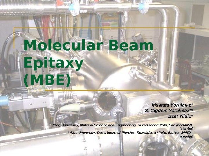
 Molecular Beam Epitaxy (MBE) Mustafa Yorulmaz* S. Çigdem Yorulmaz** Izzet Yildiz* *Koç University, Material Science and Engineering, Rumelifeneri Yolu, Sariyer-34450, Istanbul **Koç University, Department of Physics, Rumelifeneri Yolu, Sariyer-34450, Istanbul
 December 17, 2008 MASE 570 Micro and Nanofabrication, Fall 2008 2 Outline Introduction What is Epitaxy? Epitaxy Techniques Working Principle of MBE Working Conditions Setup & Operation Results and Control Mechanisms Benefits and Drawbacks of MBE Applications Conclusion
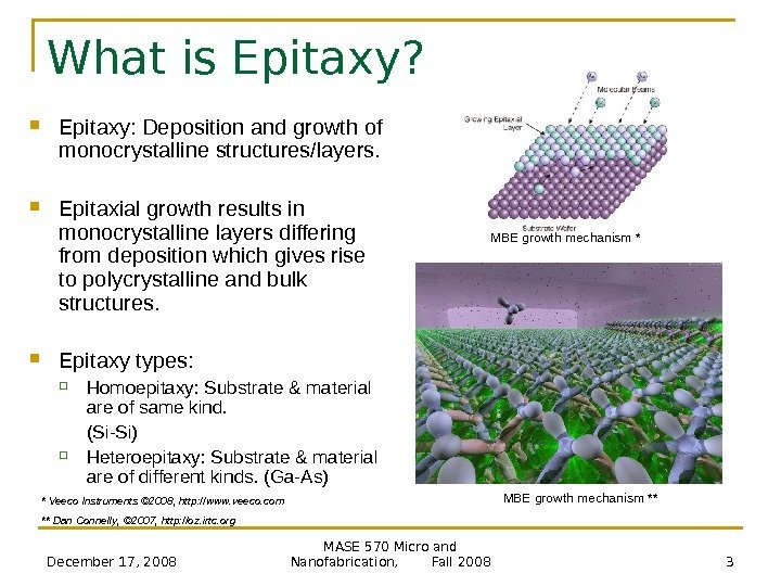
 December 17, 2008 MASE 570 Micro and Nanofabrication, Fall 2008 3 What is Epitaxy? Epitaxy: Deposition and growth of monocrystalline structures/layers. Epitaxial growth results in monocrystalline layers differing from deposition which gives rise to polycrystalline and bulk structures. Epitaxy types: Homoepitaxy: Substrate & material are of same kind. (Si-Si) Heteroepitaxy: Substrate & material are of different kinds. (Ga-As) * Veeco Instruments © 2008 , http: // www. veeco. com ** Dan Connelly , © 200 7, http: //oz. irtc. org MBE growth mechanism **
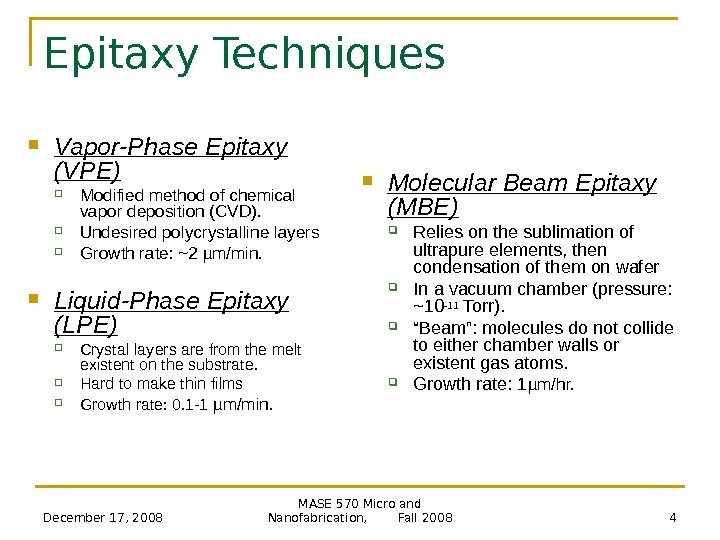
 December 17, 2008 MASE 570 Micro and Nanofabrication, Fall 2008 4 Epitaxy Techniques Vapor-Phase Epitaxy (VPE) Modified method of chemical vapor deposition (CVD). Undesired polycrystalline layers Growth rate: ~2 µ m/min. Liquid-Phase Epitaxy (LPE) Crystal layers are from the melt existent on the substrate. Hard to make thin films Growth rate: 0. 1 -1 µ m/min. Molecular Beam Epitaxy (MBE) Relies on the sublimation of ultrapure elements, then condensation of them on wafer In a vacuum chamber (pressure: ~10 -11 Torr). “ Beam”: molecules do not collide to either chamber walls or existent gas atoms. Growth rate: 1 µ m/hr.
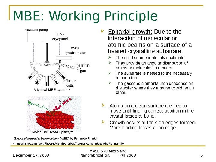
 December 17, 2008 MASE 570 Micro and Nanofabrication, Fall 2008 5 MBE: Working Principle A typical MBE system* * “Basics of molecular beam epitaxy (MBE)” by Fernando Rinaldi Epitaxial growth: Due to the interaction of molecular or atomic beams on a surface of a heated crystalline substrate. The solid source materials sublimate They provide an angular distribution of atoms or molecules in a beam. The substrate is heated to the necessary temperature. The gaseous elements then condense on the wafer where they may react with each other. Molecular Beam Epitaxy** ** http: //iramis. cea. fr/en/Phocea/Vie_des_labos/Ast/ast_sstechnique. php? id_ast=494 A toms on a clean surface are free to move until finding correct position in the crystal lattice to bond. Growth occurs at the step edges formed : M ore binding forces at an edge.
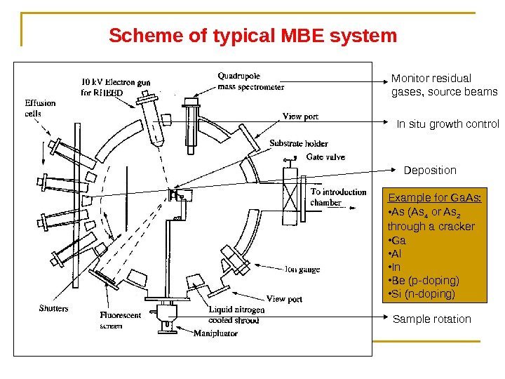
 Scheme of typical MBE system Monitor residual gases, source beams In situ growth control Sample rotation Deposition Example for Ga. As: • As (As 4 or As 2 through a cracker • Ga • Al • In • Be (p-doping) • Si (n-doping)
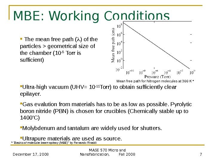
 December 17, 2008 MASE 570 Micro and Nanofabrication, Fall 2008 7 MBE: Working Conditions The mean free path ( ) of the particles > geometrical size of the chamber (10 -5 Torr is sufficient) Ultra-high vacuum (UHV= 10 -11 Torr) to obtain sufficiently clear epilayer. Gas evalution from materials has to be as low as possible. Pyrolytic boron nitride (PBN) is chosen for crucibles (Chemically stable up to 1400 ° C) Molybdenum and tantalum are widely used for shutters. Ultrapure materials are used as source. Mean free path for Nitrogen molecules at 300 K * * “Basics of molecular beam epitaxy (MBE)” by Fernando Rinaldi
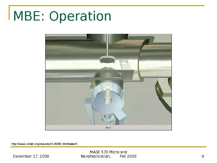
 December 17, 2008 MASE 570 Micro and Nanofabrication, Fall 2008 8 MBE: Operation http: //www. virlab. virginia. edu/VL/MBE. htm/state/
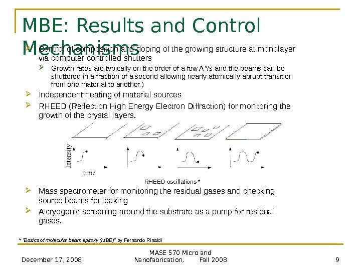
 December 17, 2008 MASE 570 Micro and Nanofabrication, Fall 2008 9 MBE: Results and Control Mechanisms RHEED oscillations * * “Basics of molecular beam epitaxy (MBE)” by Fernando Rinaldi Control of composition and doping of the growing structure at monolayer via computer controlled shutters Growth rates are typically on the order of a few A ° /s and the beams can be shuttered in a fraction of a second allowing nearly atomically abrupt transition from one material to another. ) Independent heating of material sources RHEED (Reflection High Energy Electron Diffraction) for monitoring the growth of the crystal layers. Mass spectrometer for monitoring the residual gases and checking source beams for leaking A cryogenic screening around the substrate as a pump for residual gases.
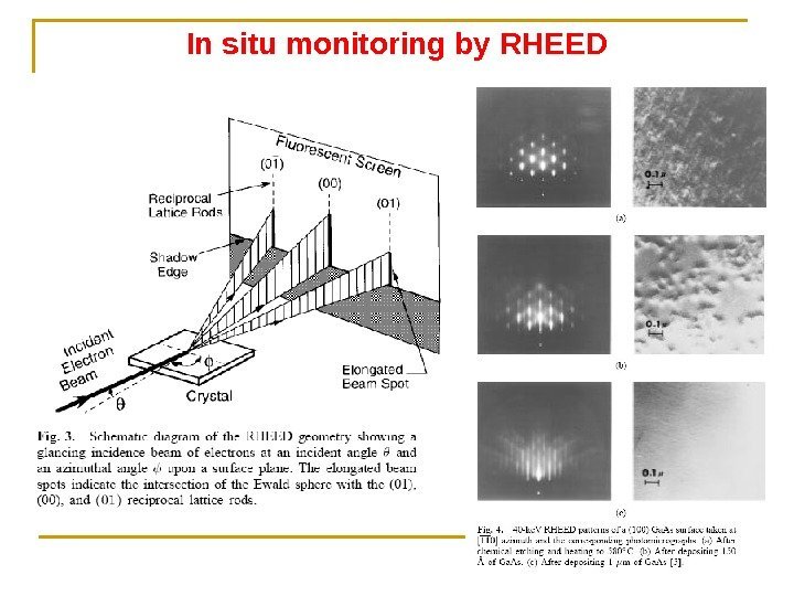
 In situ monitoring by RH
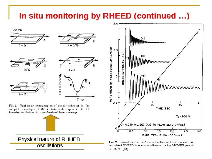
 In situ monitoring by RHEED (continued …) Physical nature of RHHED oscillations
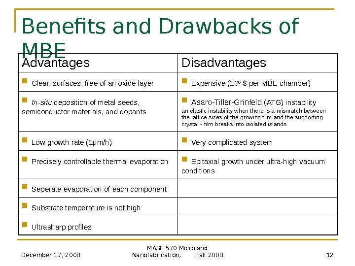
 December 17, 2008 MASE 570 Micro and Nanofabrication, Fall 2008 12 Benefits and Drawbacks of MBE Advantage s Disadvantage s Clean surfaces, free of an oxide layer Expensive (10 6 $ per MBE chamber) In-situ deposition of metal seeds, semiconductor materials, and dopants Asaro-Tiller-Grinfeld ( ATG ) instability an elastic instability when there is a mismatch between the lattice sizes of the growing film and the supporting crystal — film breaks into isolated islands Low growth rate (1 μ m/h ) Very complicated system Precisely controllable thermal evaporation Epitaxial growth under ultra-high vacuum conditions Seperate evaporation of each component Substrate temperature is not high Ultrasharp profiles
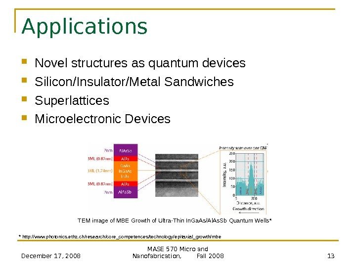
 December 17, 2008 MASE 570 Micro and Nanofabrication, Fall 2008 13 Applications Novel structures as quantum devices Silicon/Insulator/Metal Sandwiches Superlattices Microelectronic Devices TEM image of MBE Growth of Ultra — Thin In. Ga. As/Al. As. Sb Quantum Wells * * http: //www. photonics. ethz. ch/research/core_competences/technology/epitaxial_growth/mbe
 Brolis Semiconductors offers molecular beam epitaxy foundry service of custom structures using in-house multi-wafer MBE facility. Possible multi-wafer growth capacity: 14 x 2 -inch, 7 x 3 -inch, and 4 x 4 -inch. Available materials sources are Aluminium (Al), galium (Ga), indium (In), Arsenic (As) and Antimony (Sb). For doping purposes berylium (Be), silicon (Si) and galium telluride (Ga. Te) are available. In-house wafer qualificatioin includes: – HRXRD (rocking curve, reciprocal space mapping) – Photoluminescense 10 K – 300 K – Room-temperature photoluminescence mapping up to 4 -inch wafer diameter – Optical microscopy – Van der Pauw measurements for Hall mobility and carrier concentration – FTIR reflectivity measurements in the spectral range 800 nm – 15 000 nm Wafer growth, qualification and packaging is carried out in the class ISO 6 (class 1000) cleanroom environment. We have provided molecular beam epitaxy foundry service for a variety of different material combinations for a variety of applications: Ga. As/Al. Ga. As/In. Ga. As, Al. In. As/In. Ga. As/In. P, Al. Ga. As. Sb/Ga. In. As. Sb/Ga. Sb, In. As/Ga. Sb/Al. Sb, etc Our experimental room-temperature electron mobility is up to 9000 cm 2/(Vs) for Ga. In. As/Al. Ga. As/Ga. As and 26 000 cm 2/(Vs) for In. As/Al. Sb/Ga. As structures. In order to get a quotation, please send us you structure information, which would include: – Layer thickness and material compositions – Layer doping information – Desirable substrate and the size of the substrate – Allowed tolerances – Quantity of wafers
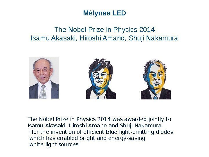
 The Nobel Prize in Physics 2014 was awarded jointly to Isamu Akasaki, Hiroshi Amano and Shuji Nakamura «for the invention of efficient blue light-emitting diodes which has enabled bright and energy-saving white light sources» Mėlynas LED The Nobel Prize in Physics 2014 Isamu Akasaki, Hiroshi Amano, Shuji Nakamura
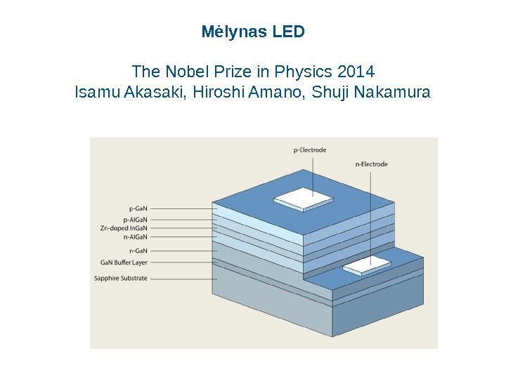
 Mėlynas LED The Nobel Prize in Physics 2014 Isamu Akasaki, Hiroshi Amano, Shuji Nakamura
 December 17, 2008 MASE 570 Micro and Nanofabrication, Fall 2008 17 Conclusions Typically in ultra-high vacuum Deposition rates are very low (1 monolayer/second) Very well controlled (Shuttering: 0. 1 s) Grow films with good crystal structure Often use multiple sources to grow alloy films Deposition rate is so low that substrate temperature doesn’t need to be as high Expensive Sophisticated system

