34c7b8ba0c9d5f85a6345de2f6a60a90.ppt
- Количество слайдов: 32
![Microcontroller Intel 8051 [Architecture] Microcontroller Intel 8051 [Architecture]](https://present5.com/presentation/34c7b8ba0c9d5f85a6345de2f6a60a90/image-1.jpg) Microcontroller Intel 8051 [Architecture]
Microcontroller Intel 8051 [Architecture]
 The Microcontroller • Microcontrollers can be considered as self-contained systems with a processor, memory and I/O ports. – In most cases, all that is missing is the software to define the operation of the embedded system. • Usually available in several forms: – Devices for prototyping • Built-in or piggy-back EPROM for storing the software. – One Time Programmable (OTP) devices. • No window on the package. Therefore, the internal EPROM cannot be erased after being programmed. – High Volume Production devices. • Use ROM internally to hold the software. Cheaper in large volume.
 The Architectural Needs of a Microcontroller • Lets consider what architectural features would be needed in a microcontroller. • What are the expected applications? – Sensing the environment (Input) – Producing a response (Output) – The response may be delayed (Timer/Counter) – Prioritized response (Interrupts) – Software to control the process (Non-volatile Memory) – Temporary data (RAM)
 Major Microcontroller Families • There are several major “families” of microcontrollers available from different manufacturers. – A family is defined as a group of products that share the same basic internal architectures and who are code -compatible. – Manufacturers usually define an architecture and then make variants of that design producing a family of products. – Code written for a member of the family should be compatible with all other members of the same family.
 Example Microcontroller Families • Z 80 from Zilog – 8 -bit microprocessor based on the 8080 architecture. – Capable of 1 MIP at 4 MHz. – Accumulator, 6 8 -bit registers, 2 index registers. – Uses external RAM for temporary data. – Built-in refresh circuitry for the external RAM. – Only port-based I/O. – Slowly disappearing.
 Example Microcontroller Families …Cont. • MC 6811 from Motorola – 8 -bit stack-based architecture. – 2 accumulators and 2 index registers. – Built in EEPROM and RAM. – Digital I/O. – Timers. – ADC. – RS 232 communication. – Was the most powerful and flexible controller available at introduction. • Around 1970. – Still very popular.
 The MCS-51 Family of Microcontrollers • Originally introduced by Intel in 1981. – Currently, the most widely used microcontroller. – 8 -bit processor. – 2 distinct separately addressable memory areas. • Maximum of 64 K on-chip ROM. – Usually 0 to 4 K. • Maximum of 64 K external data memory. • Maximum of 64 K external code memory. • Basic version (8051) contains: – 4 K Bytes of on-chip ROM instruction memory. – 128 Bytes of on-chip RAM for temporary data storage and the stack. – 2 timers, one serial port, and four 8 -bit parallel I/O ports. – Speeds starting from 12 MHz.
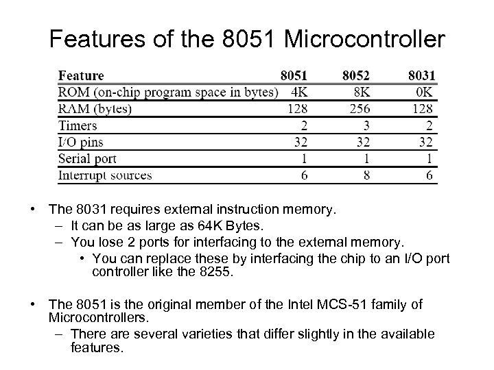 Features of the 8051 Microcontroller • The 8031 requires external instruction memory. – It can be as large as 64 K Bytes. – You lose 2 ports for interfacing to the external memory. • You can replace these by interfacing the chip to an I/O port controller like the 8255. • The 8051 is the original member of the Intel MCS-51 family of Microcontrollers. – There are several varieties that differ slightly in the available features.
 Manufacturers of MCS-51 Clones • There is a large number of companies that manufacture microcontrollers in the 8051 family. – ATMEL Corporation. • Flash instead of EPROM. • Low Voltage. • Minimal version with less memory and fewer I/O ports in a smaller package. • CMOS implementation. • Speeds that range from 12 to 20 MHz.
 Manufacturers of MCS-51 Clones – Dallas Semiconductor • Uses NV-RAM. Programmable in-system. • As large as 32 K of instruction memory. • Some versions have an on-chip real-time clock. – Philips Corporation. • Large selection of 8051 based microcontrollers. • Include features like A/D and D/A on chip. – Xilinx and Altera • 8051 FPGA cores.
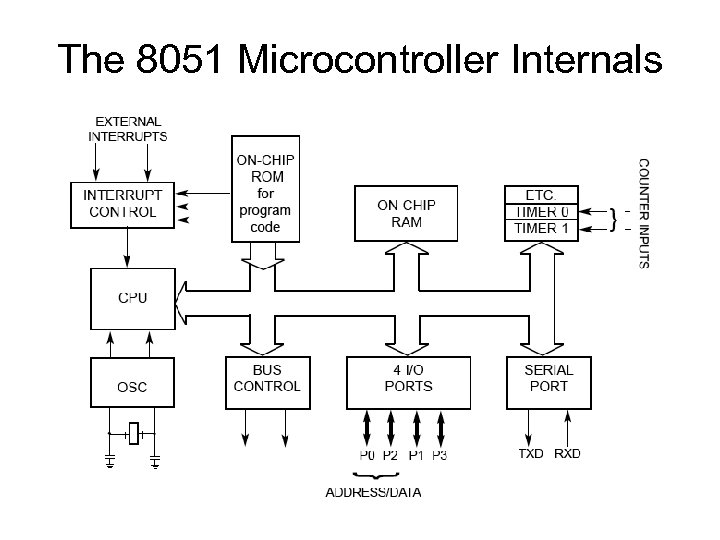 The 8051 Microcontroller Internals
 8051 Architecture • Programmer’s View – Memory Organization – Register Set – Instruction Set • Hardware Designer’s View – Pin-out – Timing characteristics – Current / Voltage requirements
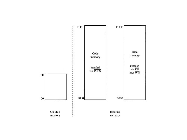
 Memory Organization The 8051 has separate address spaces for program storage and data storage. – Depending on the type of instruction, the same address can refer to two logically and physically different memory locations.
 Program Storage • After reset, the MCS-51 starts fetching instructions from 0000 H. – This can be either on-chip or external depending on the value of the EA input pin. • If EA* is low, then the program memory is external. • If EA* is high, then addresses from 0000 to 0 FFF will refer to on-chip memory and addresses 1000 up to FFFF refer to external memory. – Note that the 8031 must have its EA connected low as all of its memory is external. Link: EA connection
 Access to External Memory • Port 0 acts as a multiplexed address/data bus. Sending the low byte of the program counter (PCL) as an address. • Port 2 sends the program counter high byte (PCH) directly to the external memory. • The signal ALE operates as in the 8051 to allow an external latch to store the PCL byte while the multiplexed bus is made ready to receive the code byte from the external memory. • Port 0 then switches function and becomes the data bus receiving the byte from memory. Link: H/w Interfacing
 Data Storage • The 8051 has 256 bytes of RAM on-chip. – The lower 128 bytes are intended for internal data storage. – The upper 128 bytes are the Special Function Registers (SFR). • The lower 128 bytes are not to be used as standard RAM. – Internally 8051’s registers default to stack area, and other features. [00 -7 FH] Link: Memory Organization
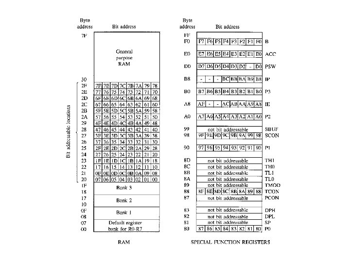
![Data Storage [Cont. . . ] • The lowest 32 bytes of the on-chip Data Storage [Cont. . . ] • The lowest 32 bytes of the on-chip](https://present5.com/presentation/34c7b8ba0c9d5f85a6345de2f6a60a90/image-17.jpg) Data Storage [Cont. . . ] • The lowest 32 bytes of the on-chip RAM form 4 banks of 8 registers each. • Only one of these banks can be active at any time. • Bank is chosen by setting 2 bits in PSW – Default bank (at power up) is bank 0 (locations 00 – 07). • The 8 registers in any active bank are referred to as R 0 through R 7 • Given that each register has a specific address, it can be accessed directly using that address even if its bank is not the active one.
Data Storage [Cont. . . ] • The lowest 32 bytes of the on-chip RAM form 4 banks of 8 registers each. • Only one of these banks can be active at any time. • Bank is chosen by setting 2 bits in PSW – Default bank (at power up) is bank 0 (locations 00 – 07). • The 8 registers in any active bank are referred to as R 0 through R 7 • Given that each register has a specific address, it can be accessed directly using that address even if its bank is not the active one.
![Data Storage [Cont. . . ] • The next 16 bytes – locations 20 Data Storage [Cont. . . ] • The next 16 bytes – locations 20](https://present5.com/presentation/34c7b8ba0c9d5f85a6345de2f6a60a90/image-18.jpg) Data Storage [Cont. . . ] • The next 16 bytes – locations 20 H to 2 FH – form a block that can be addressed as either bytes or individual bits. – The bytes have addresses 20 H to 2 FH. – The bits have addresses 00 H to 7 FH. – Specific instructions are used for accessing the bits. • Locations 30 H to 7 FH are general purpose RAM. Link: Memory Organization
Data Storage [Cont. . . ] • The next 16 bytes – locations 20 H to 2 FH – form a block that can be addressed as either bytes or individual bits. – The bytes have addresses 20 H to 2 FH. – The bits have addresses 00 H to 7 FH. – Specific instructions are used for accessing the bits. • Locations 30 H to 7 FH are general purpose RAM. Link: Memory Organization
 The SFR (Special Function Register) • The upper 128 bytes of the on-chip RAM are used to house special function registers. • In reality, only about 25 of these bytes are actually used. The others are reserved for future versions of the 8051. – These are registers associated with important functions in the operation of the MCS-51. – Some of these registers are bit-addressable as well as byteaddressable. • The address of bit 0 of the register will be the same as the address of the register.
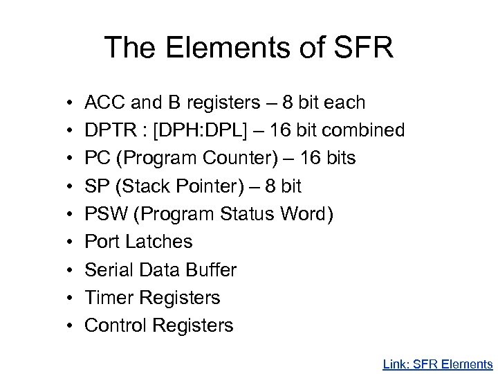 The Elements of SFR • • • ACC and B registers – 8 bit each DPTR : [DPH: DPL] – 16 bit combined PC (Program Counter) – 16 bits SP (Stack Pointer) – 8 bit PSW (Program Status Word) Port Latches Serial Data Buffer Timer Registers Control Registers Link: SFR Elements
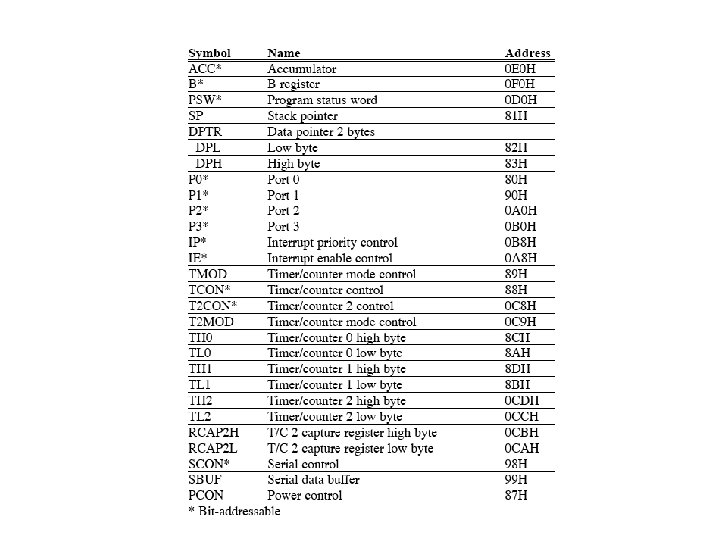
 The ACC – Accumulator • Commonly used for move and arithmetic instructions. • Can be referred to in several ways: – Implicitly in op-codes. – Referred to as ACC (or A) for instructions that allow specifying a register. – By its SFR address 0 E 0 H. • Operates in a similar manner to the 8085 accumulator. • Bit addressable. – ACC. 2 means bit 2 of the ACC register.
 The B Register • Commonly used as a temporary register, much like a 9 th R register. • Used by two op-codes – MUL AB, div AB • B register holds the second operand will hold part of the result – Upper 8 bits of the multiplication result – Remainder in case of division. • Can also be accessed through its SFR address of 0 F 0 H. • Bit addressable.
 The DPL and DPH Registers • 2 8 -bit registers that can be combined into a 16 -bit DPTR – Data Pointer. • Used by commands that access external memory • Also used for storing 16 bit values mov DPTR, #data 16 ; setup DPTR with 16 bit ext address movx A, @DPTR ; copy mem[DPTR] to A • Can be accessed as 2 separate 8 -bit registers if needed. • DPTR is useful for string operations and Look-Up-Table (LUT) operations.
 The SP Register • SP is the stack pointer. • SP points to the last used location of the stack. – Push operation will first increment SP and then copy data. – Pop operation will first copy data and then decrement SP. • In 8051, stack grows upwards (from low memory to high memory) and can be in the internal RAM only. • On power-up, SP points to 07 H. – Register banks 2, 3, 4 (08 H to 1 FH) form the default stack area. • Stack can be relocated by setting SP to the upper memory area in 30 H to 7 FH. – mov SP, #32 H
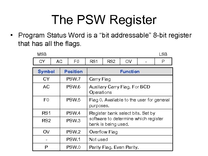 The PSW Register • Program Status Word is a “bit addressable” 8 -bit register that has all the flags. MSB CY LSB AC F 0 RS 1 RS 2 OV - P Symbol Position Function CY PSW. 7 Carry Flag AC PSW. 6 Auxiliary Carry Flag. For BCD Operations F 0 PSW. 5 Flag 0. Available to the user for general purposes. RS 1 PSW. 4 RS 2 PSW. 3 Register bank select bits. Set by software to determine which register bank is being used. OV PSW. 2 Overflow Flag - PSW. 1 Not used P PSW. 0 Parity Flag. Even Parity.
 The P 0, P 1, P 2, and P 3 Registers • Port Latches. • Specify the value to be output on the specific output port or the value read from the specific input port. • Bit addressable. – First bit has the same address as the register. – Example: P 1 has address 90 H in the SFR, so • P 1. 7 or address 97 H refer to the same bit. Link: SFR address
 The SBUF Register • Serial Port Data Buffer. • 2 registers at the same location – One is read-only used for reading serial input data. • Serial Data Receive Buffer. – The other is write-only used for storing serial output data. • Serial Data Transmit Buffer. Link: SFR address
 Timer Registers – TH 0 and TL 0 • The high and low bytes of the 16 -bit counting register for timer/counter T 0. • There is also a TH 1 / TL 1 pair for the T 1 timer. • In the 8052, one more pair exists (TH 2) / (TL 2) for the T 2 timer. • (RCAP 2 H) and (RCAP 2 L) exist only in the 8052 and they are copies of the TH 2 and TL 2 registers. Link: SFR address
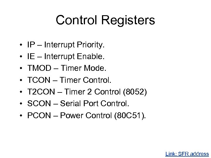 Control Registers • • IP – Interrupt Priority. IE – Interrupt Enable. TMOD – Timer Mode. TCON – Timer Control. T 2 CON – Timer 2 Control (8052) SCON – Serial Port Control. PCON – Power Control (80 C 51). Link: SFR address


