cc47c5f48f51cc1e764b60caecab54ad.ppt
- Количество слайдов: 39


Microchip Fabrication A Practical Guide to Semiconductor Processing 半導體製程 材料科學與 程研究 所 張翼 教授

Chapter 1 The Semiconductor Industry

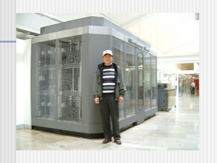
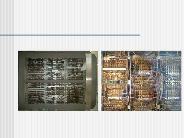
Figure 1. 1 Eniac statistics. (Foundations of Computector Technology, J. G. Giarratano, Howard W. Sams & Co. , Indianapolis, Ind. , 1983) (First electronic computer, 1947)
 → Transistor")
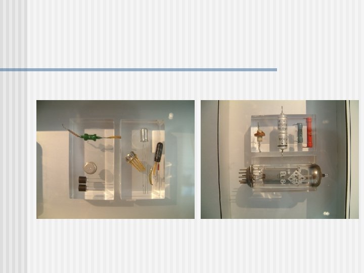
Figure 1. 2 Vacuum tube n n Vacuum tube (better radiation hardening) → Transistor NCTU is the first University to use transistor in student Lab. →
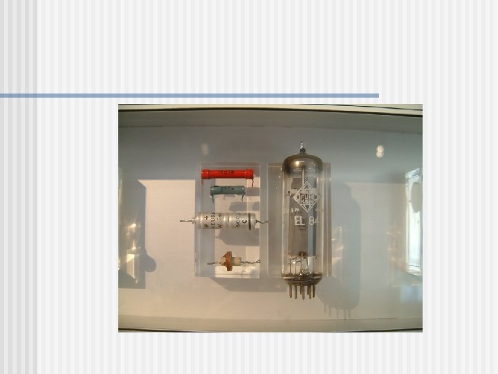

Figure 1. 3 The first transistor. n n Bell Labs John Bardeen, Walter Brattin, William Shockley 1956 Nobel Prize (Physicist) Si-Ge, bandgap increase, low terminal noise
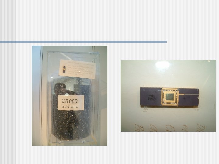

Figure 1. 4 Solid-state discrete devices. n n n active device: transistors & diodes passive element: capacitors & resistors Discrete device account for 12% sale in 1998
")
Figure 1. 5 Kilby integrated circuit from his notebook (Courtesy of Texas Instruments. ) n In 1959, TI developed first IC. (Jack Kilby)

Figure 1. 6 Horni “teardrop” transistor. n Planar Technology

Figure 1. 7 Growth of Dram Density (After Campbell, The Science of Engineering and Microelectronics fabrication, Oxford Press. ) n n First demo, Bell Labs First production, NEC
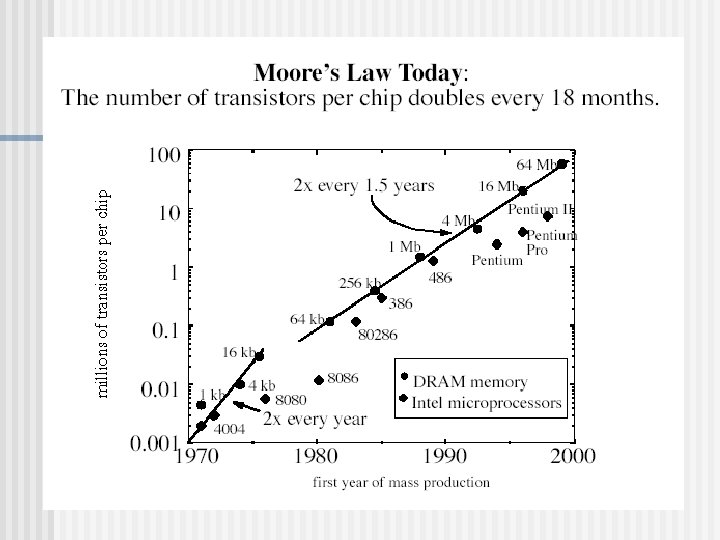
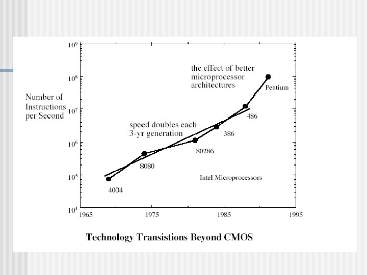

Figure 1. 8 IC integration table.

Figure 1. 9 Decreasing image feature size. (After Wolf and Tauber, “Silicon Processing for the VSLI Era. ”) n 2000, 0. 18µm, TSMC 2012, 0. 005µm

Figure 1. 10 Effect of processing larger die on larger wafers. n n wafer size → 12 inch (1 B USD to build) ULSI chip size> 0. 5 inch each side # whole die in a wafer : 40 → Need to decrease contamination use class 1 clean room

Figure 1. 11 Relative size of airborne particles and wafer dimensions. n n n class 1 1 Particle/ft 3 Particle size < 0. 1µm

Figure 1. 12 Cross section of typical planarized two-level metal VLI structure showing range of via depths after planarization. (Courtesy of Solid State Technology) n Use multilayer interconnect level to increase traffic
.")
Figure 1. 13 Wafer fabrication (and electrical test).
: Doubling")
Figure 1. 14 Price of chips per bit of memory. Moore’s law (1965): Doubling of transistors in the ICs every couple of years 1971 2250 1982 120, 000 1993 3, 100, 000 2000 42, 000
 n original driving")
Figure 1. 15 Semiconductor chip uses. (Courtesy In-Stat-1995 SEMI ISS seminary) n original driving force: military demand
 → semiconductor")
Figure 1. 16 Semiconductor and vehicle parts growth (Courtesy Semiconductor Industry Association) → semiconductor → motor vehicle parts
")
Figure 1. 17 Future DRAM capacity. (Source: Business Week, July, 1994)
 →")
Figure 1. 18 Growth of semiconductor industry-capital spending (Courtesy of Semiconductor Industry Association) → semiconductors

Figure 1. 18 n n n n Wafer Fabrication Vertical Integration IDM: Integrated Device Manufacturer-include IC design and manufacture Fabless company Foundry Captive: produce in house for their own use Merchant supplier: sell to the open market

Figure 1. 19 Stages of semiconductor manufacturing.

Figure 1. 20 Conversion of silicon dioxide to semiconductor grade silicon.

Figure 1. 21 Crystal growth and wafer preparation.
")
Figure 1. 22 Wafer fabrication (and electrical test)

Figure 1. 23 Packaging stage. n Packaging technology becomes important as CPU speed approaching 1 Gb/Sec

Figure 1. 24 P-N and N-P junctions.

Figure 1. 25 Basics of silicon planar processing.

Figure 1. 26 Double diffused bipolar transistor formed in epitaxial layer.

Figure 1. 27 DRAM growth design rule and number of process steps. (SEMI 1995 ISS Conference)
cc47c5f48f51cc1e764b60caecab54ad.ppt