f0af42b1e6170b41a4d83bca1f292c27.ppt
- Количество слайдов: 45
 Micro-diffractive nanostructures for cold-atom manipulation (and other interesting stuff) Groupe optique atomique et applications aux nanostructures Université Paul Sabatier—CNRS Toulouse, France FRISNO-8 Ein-Bokek, Israel February 20 -25, 2005 http: //www. nanocold. cict. fr http: //www. fastnet. fr
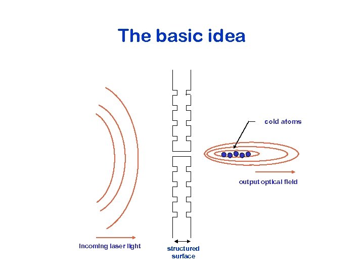 The basic idea cold atoms output optical field incoming laser light structured surface
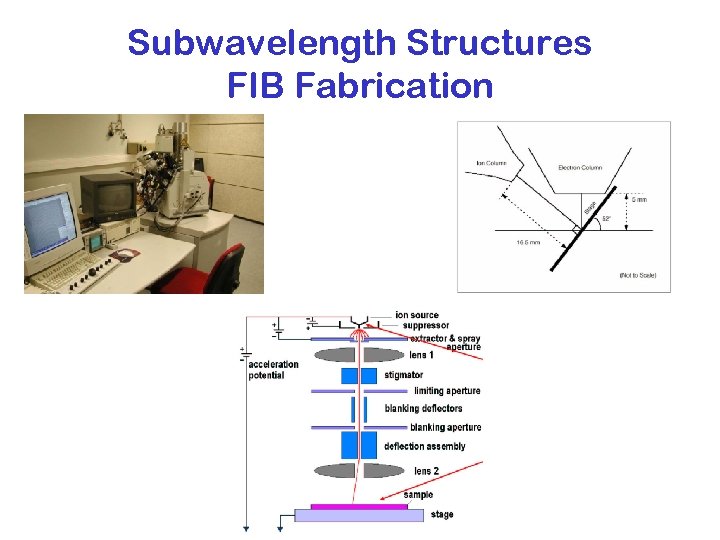 Subwavelength Structures FIB Fabrication
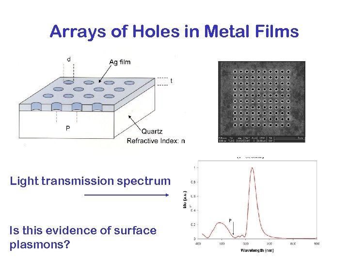 Arrays of Holes in Metal Films Light transmission spectrum Is this evidence of surface plasmons?
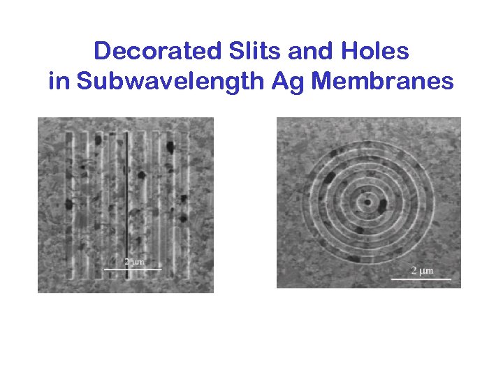 Decorated Slits and Holes in Subwavelength Ag Membranes
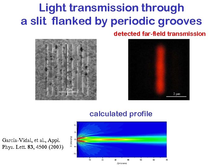 Light transmission through a slit flanked by periodic grooves detected far-field transmission calculated profile Garcia-Vidal, et al. , Appl. Phys. Lett. 83, 4500 (2003)
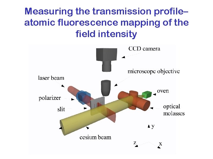 Measuring the transmission profile– atomic fluorescence mapping of the field intensity
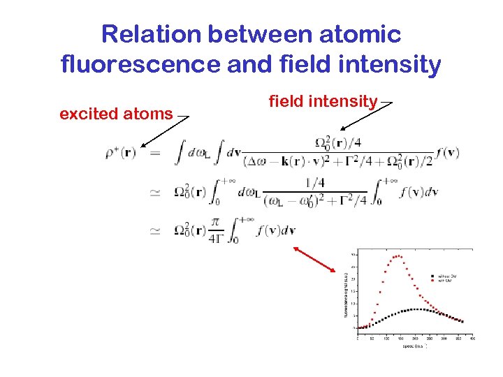 Relation between atomic fluorescence and field intensity excited atoms field intensity
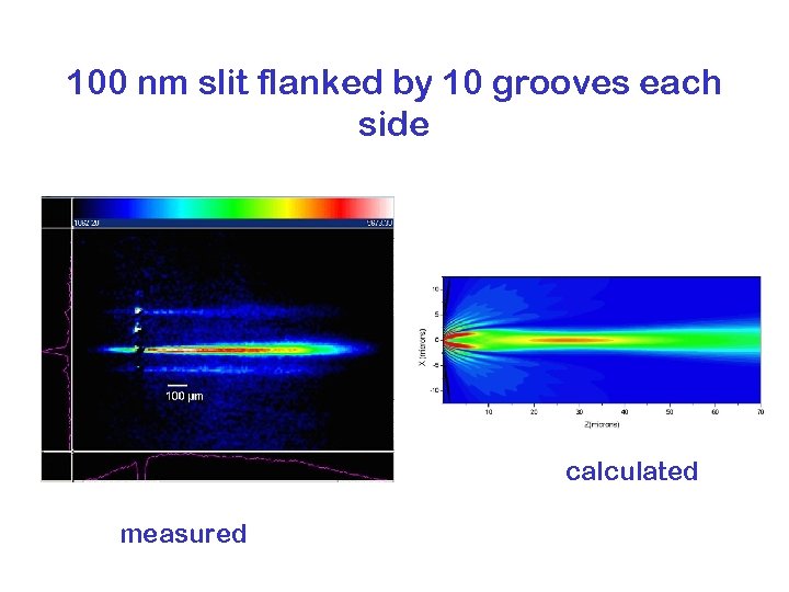 100 nm slit flanked by 10 grooves each side calculated measured
 How does the slit/groove structure produce the observed field distributions?
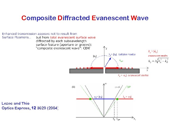 Composite Diffracted Evanescent Wave Lezec and Thio Optics Express, 12 3629 (2004)
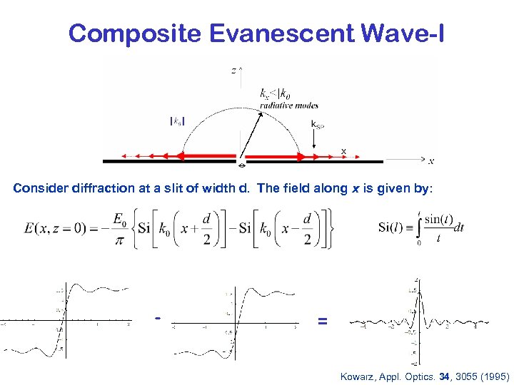 Composite Evanescent Wave-I Consider diffraction at a slit of width d. The field along x is given by: - = Kowarz, Appl. Optics. 34, 3055 (1995)
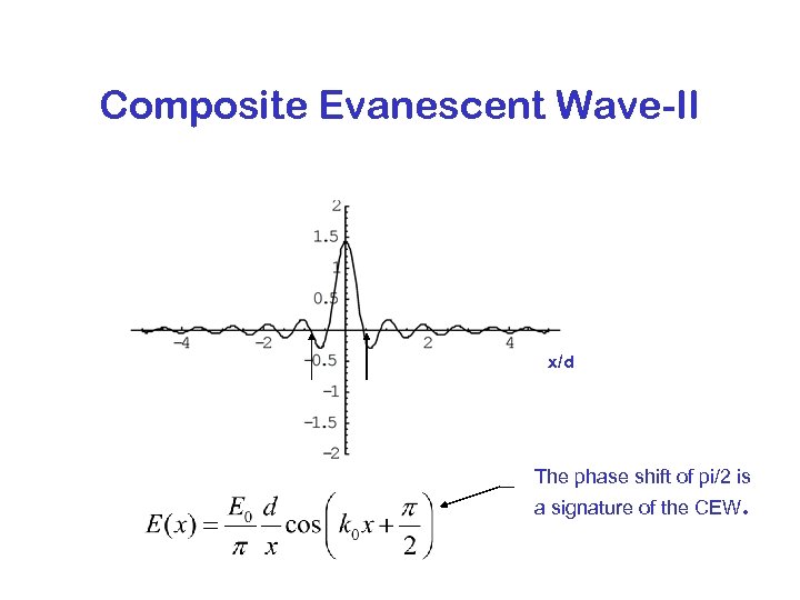 Composite Evanescent Wave-II x/d The phase shift of pi/2 is a signature of the CEW.
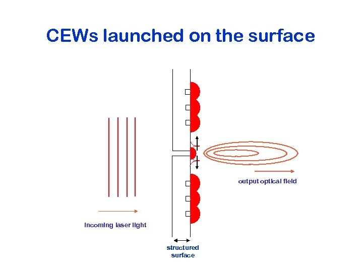 CEWs launched on the surface output optical field incoming laser light structured surface
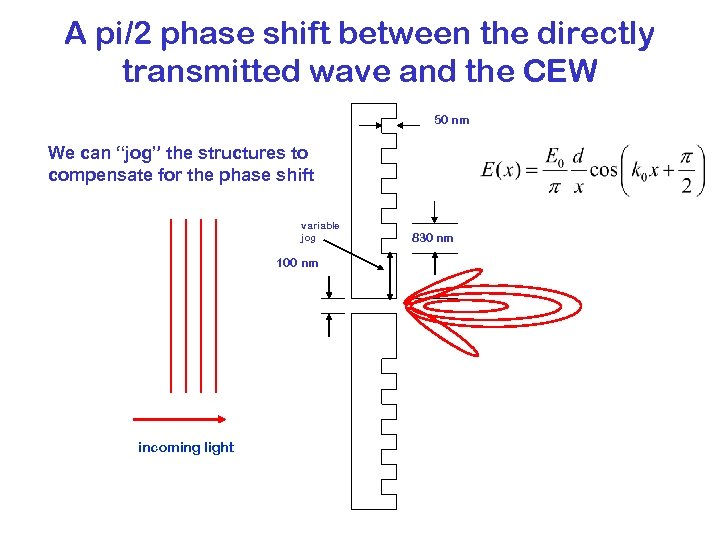 A pi/2 phase shift between the directly transmitted wave and the CEW 50 nm We can “jog” the structures to compensate for the phase shift variable jog 100 nm incoming light 830 nm
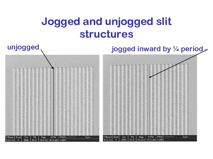 Jogged and unjogged slit structures unjogged inward by ¼ period
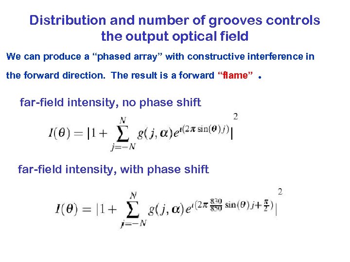 Distribution and number of grooves controls the output optical field We can produce a “phased array” with constructive interference in the forward direction. The result is a forward “flame” far-field intensity, no phase shift far-field intensity, with phase shift .
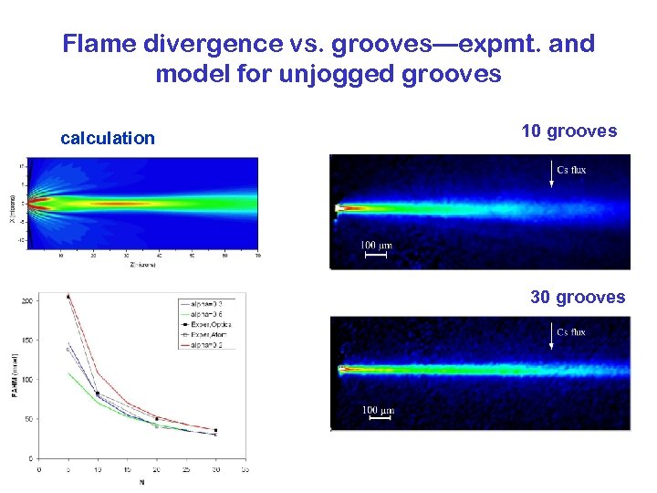 Flame divergence vs. grooves—expmt. and model for unjogged grooves calculation 10 grooves 30 grooves
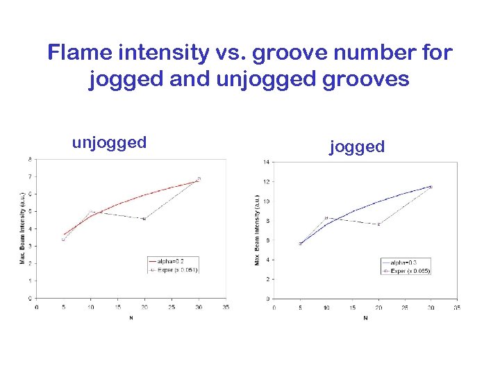 Flame intensity vs. groove number for jogged and unjogged grooves unjogged
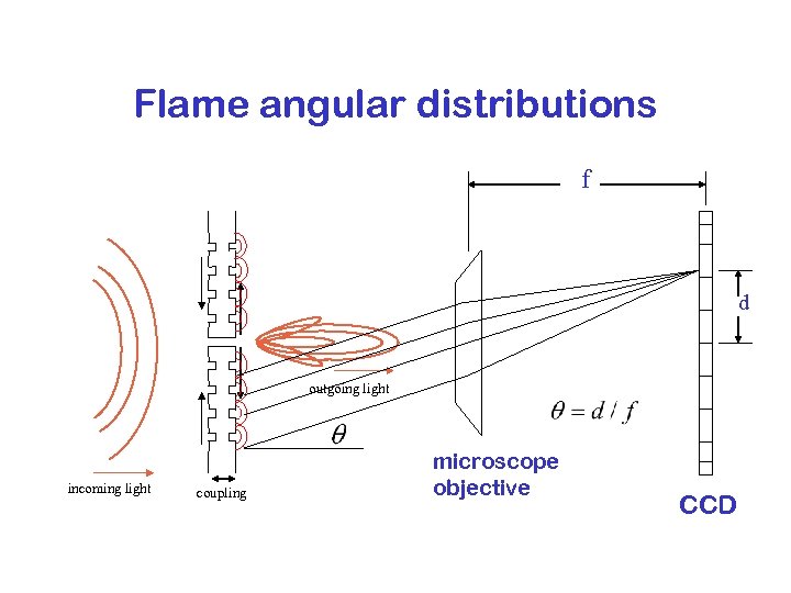 Flame angular distributions f d outgoing light incoming light coupling microscope objective CCD
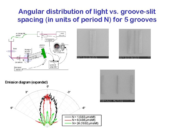 Angular distribution of light vs. groove-slit spacing (in units of period N) for 5 grooves
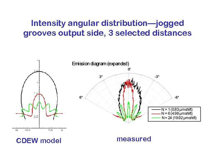 Intensity angular distribution—jogged grooves output side, 3 selected distances CDEW model measured
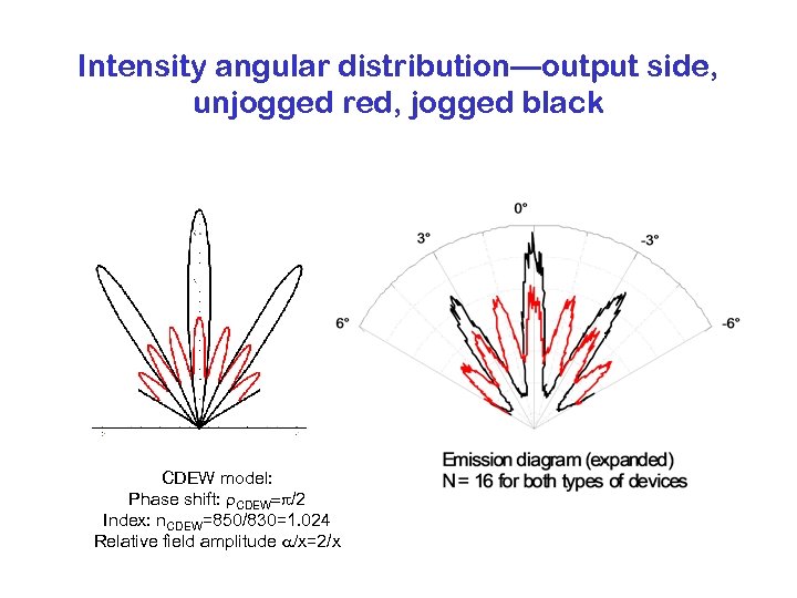 Intensity angular distribution—output side, unjogged red, jogged black CDEW model: Phase shift: r. CDEW=p/2 Index: n. CDEW=850/830=1. 024 Relative field amplitude a/x=2/x
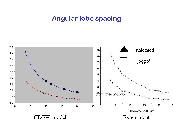 Angular lobe spacing unjogged CDEW model Experiment
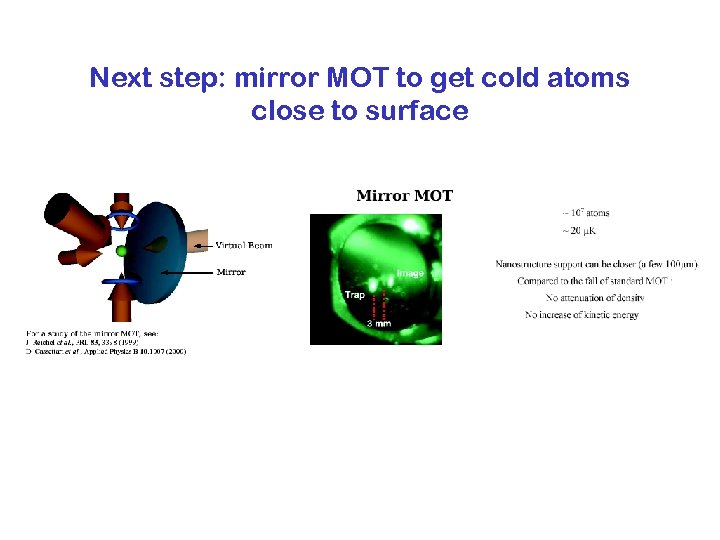 Next step: mirror MOT to get cold atoms close to surface
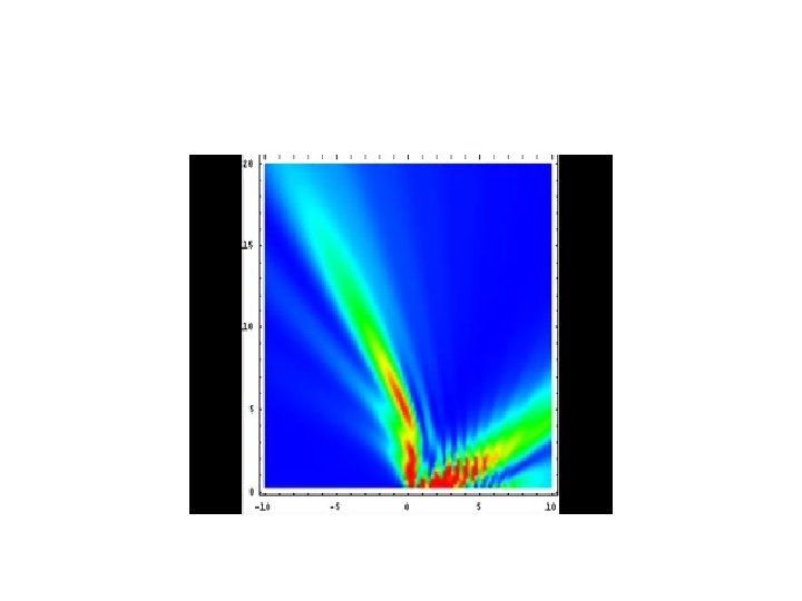
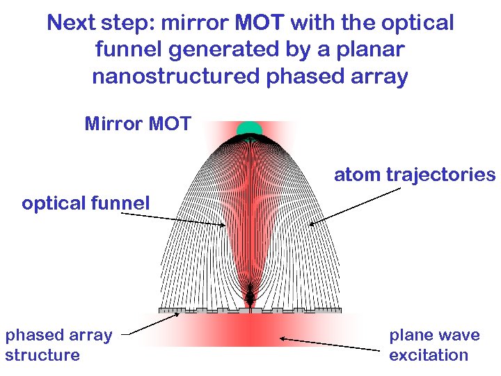 Next step: mirror MOT with the optical funnel generated by a planar nanostructured phased array Mirror MOT atom trajectories optical funnel phased array structure plane wave excitation
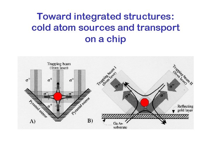 Toward integrated structures: cold atom sources and transport on a chip
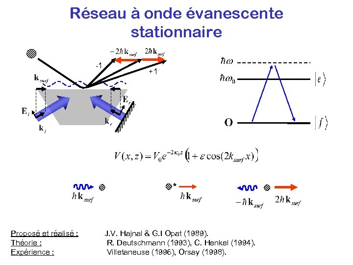
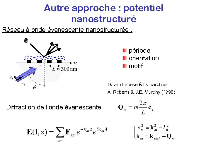
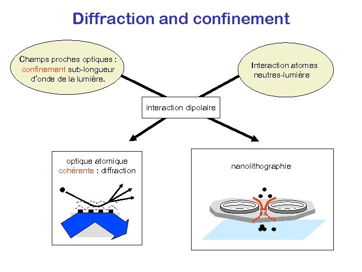 Diffraction and confinement Champs proches optiques : confinement sub-longueur d’onde de la lumière. Interaction atomes neutres-lumière interaction dipolaire optique atomique cohérente : diffraction nanolithographie
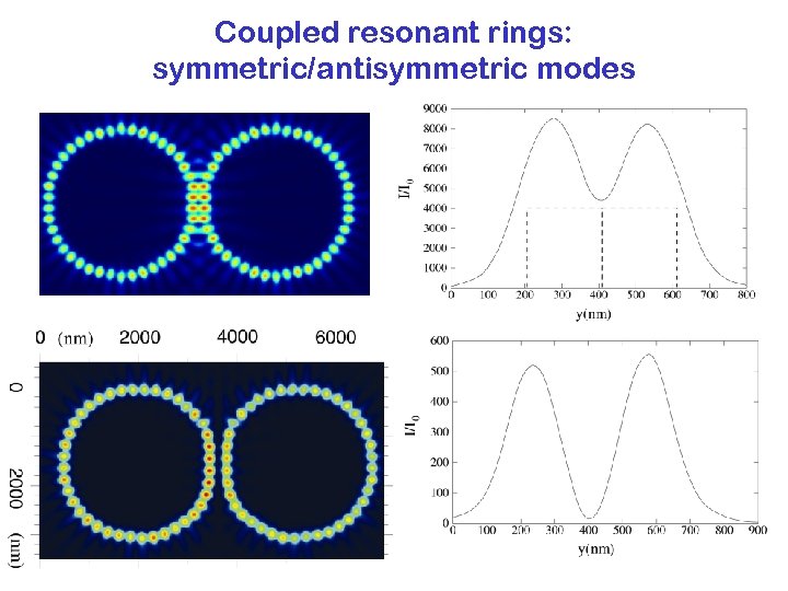 Coupled resonant rings: symmetric/antisymmetric modes
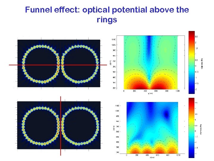 Funnel effect: optical potential above the rings
 Réseau à onde évanescente stationnaire -1 +1 * Proposé et réalisé : Théorie : Expérience : J. V. Hajnal & G. I Opat (1989). R. Deutschmann (1993), C. Henkel (1994). Villetaneuse (1996), Orsay (1998).
 Autre approche : potentiel nanostructuré Réseau à onde évanescente nanostructurée : période orientation motif D. van Labeke & D. Barchiesi A. Roberts & J. E. Murphy (1996) Diffraction de l’onde évanescente :
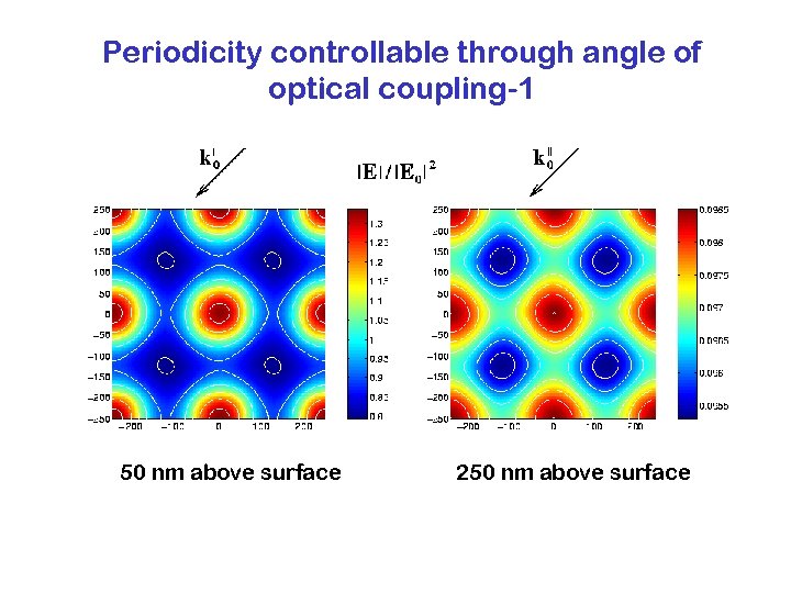 Periodicity controllable through angle of optical coupling-1 50 nm above surface 250 nm above surface
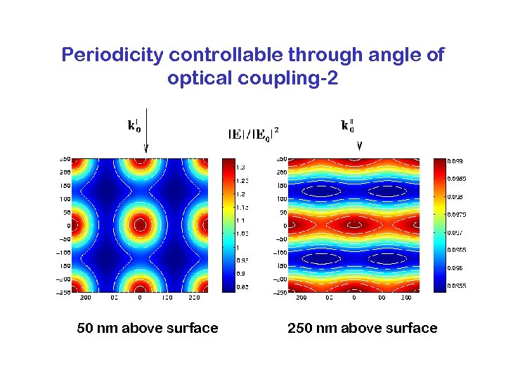 Periodicity controllable through angle of optical coupling-2 50 nm above surface 250 nm above surface
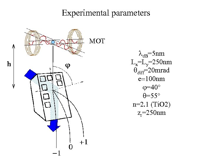 Experimental parameters MOT ld. B=5 nm Lx=Ly=250 nm qdiff=20 mrad e=100 nm j=40° q=55° n=2. 1 (Ti. O 2) zr=250 nm
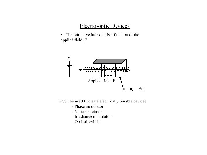
 Tales from the future—nanophotonics, addressable atom manipulation with optical arrays
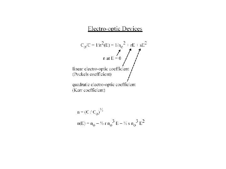
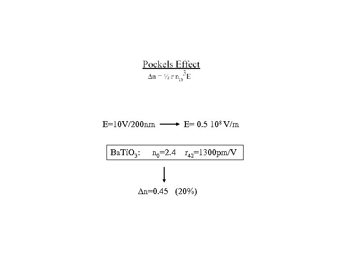 E=10 V/200 nm Ba. Ti. O 3: n 0=2. 4 E= 0. 5 108 V/m r 42=1300 pm/V Dn=0. 45 (20%)
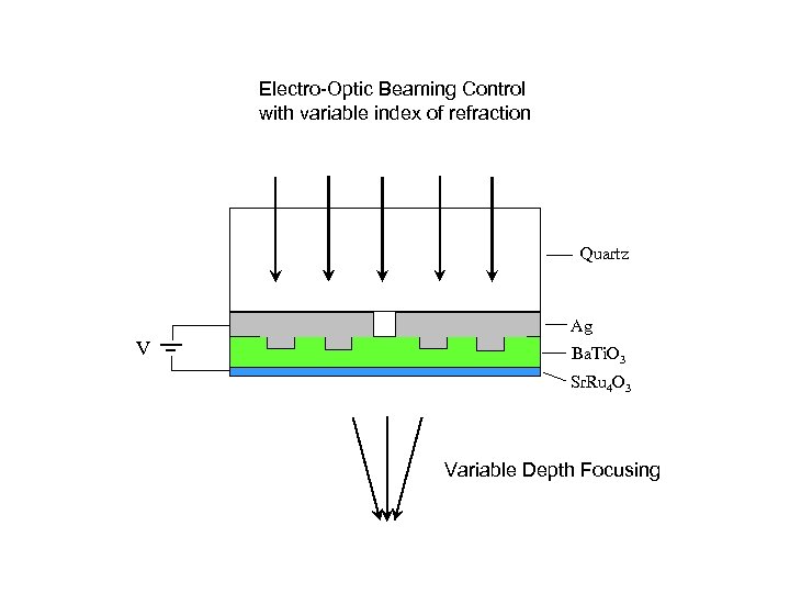 Electro-Optic Beaming Control with variable index of refraction Quartz Ag V Ba. Ti. O 3 Sr. Ru 4 O 3 Variable Depth Focusing
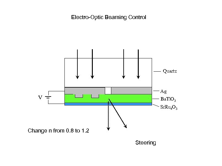 Electro-Optic Beaming Control Quartz Ag V Ba. Ti. O 3 Sr. Ru 4 O 3 Change n from 0. 8 to 1. 2 Steering
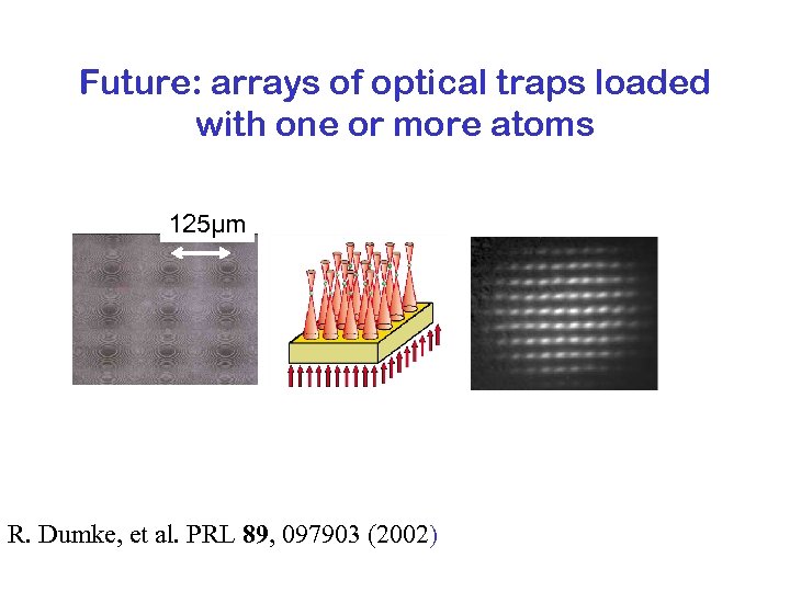 Future: arrays of optical traps loaded with one or more atoms 125µm R. Dumke, et al. PRL 89, 097903 (2002)
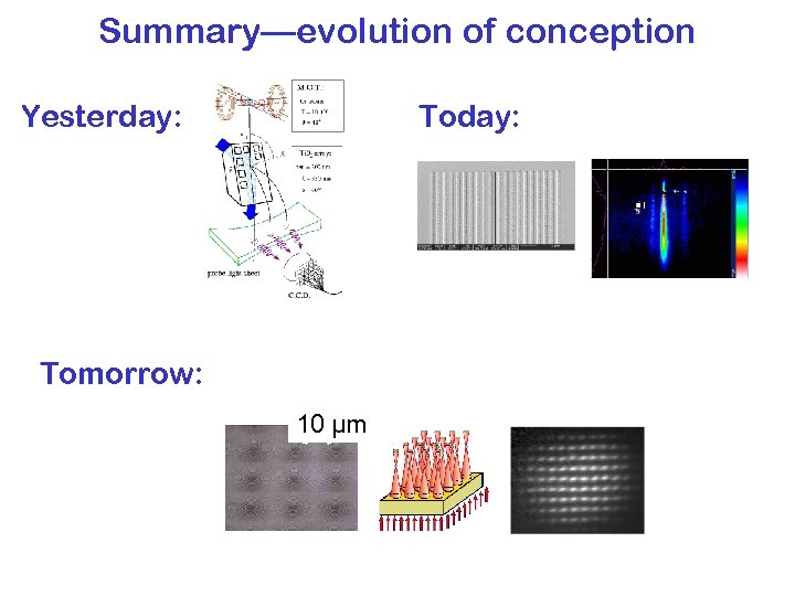 Summary—evolution of conception Yesterday: Tomorrow: 10 µm
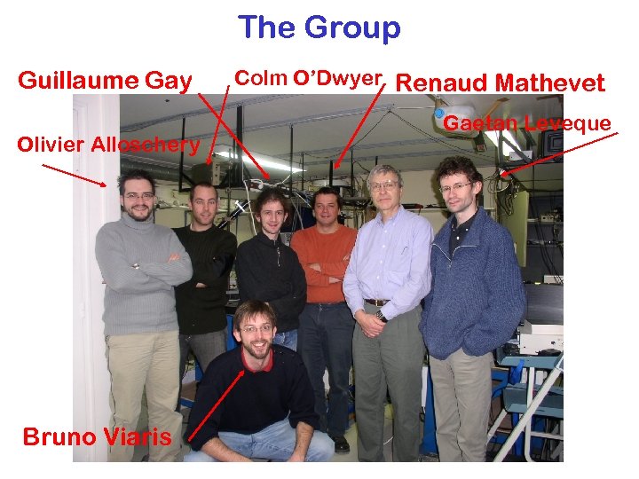 The Group Guillaume Gay Olivier Alloschery Bruno Viaris Colm O’Dwyer Renaud Mathevet Gaetan Leveque


