20f14605f54420c82490ec9bfa9301f2.ppt
- Количество слайдов: 60
 Memory Devices and Interfacing – (Chapter 9) Dr. Costas Kyriacou and Dr. Konstantinos Tatas ACOE 255 Microprocessors I - Frederick University
 Outline • Semiconductor Memory Basic Concepts • Read Only Memory (ROM) • Random Access Memory (RAM) – SRAM – DRAM • Memory Interfacing – Address size expansion – Word size expansion • Timing Analysis ACOE 255 Microprocessors I - Frederick University 2
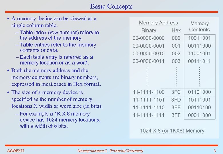 Basic Concepts • A memory device can be viewed as a single column table. – Table index (row number) refers to the address of the memory. – Table entries refer to the memory contents or data. – Each table entry is referred as a memory location or as a word. • Both the memory address and the memory contents are binary numbers, expressed in most cases in Hex format. • The size of a memory device is specified as the number of memory locations X width or word size (in bits). – For example a 1 K X 8 memory device has 1024 memory locations, with a width of 8 bits. ACOE 255 Microprocessors I - Frederick University 3
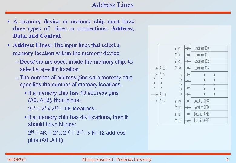 Address Lines • A memory device or memory chip must have three types of lines or connections: Address, Data, and Control. • Address Lines: The input lines that select a memory location within the memory device. – Decoders are used, inside the memory chip, to select a specific location – The number of address pins on a memory chip specifies the number of memory locations. • If a memory chip has 13 address pins (A 0. . A 12), then it has: 213 = 23 X 210 = 8 K locations. • If a memory chip has 4 K locations, then it should have N pins: 2 N = 4 K = 22 X 210 = 212 N=12 address pins (A 0. . A 11) ACOE 255 Microprocessors I - Frederick University 4
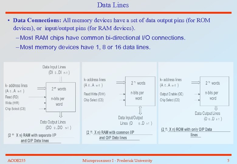 Data Lines • Data Connections: All memory devices have a set of data output pins (for ROM devices), or input/output pins (for RAM devices). – Most RAM chips have common bi-directional I/O connections. – Most memory devices have 1, 8 or 16 data lines. ACOE 255 Microprocessors I - Frederick University 5
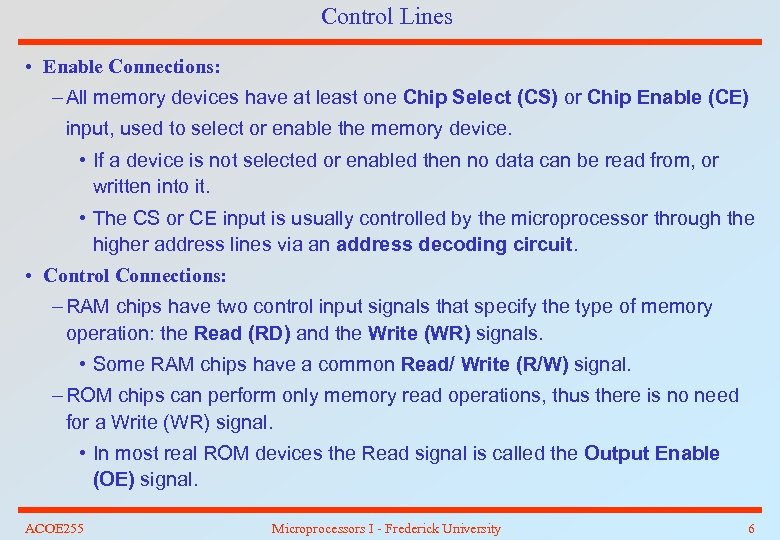 Control Lines • Enable Connections: – All memory devices have at least one Chip Select (CS) or Chip Enable (CE) input, used to select or enable the memory device. • If a device is not selected or enabled then no data can be read from, or written into it. • The CS or CE input is usually controlled by the microprocessor through the higher address lines via an address decoding circuit. • Control Connections: – RAM chips have two control input signals that specify the type of memory operation: the Read (RD) and the Write (WR) signals. • Some RAM chips have a common Read/ Write (R/W) signal. – ROM chips can perform only memory read operations, thus there is no need for a Write (WR) signal. • In most real ROM devices the Read signal is called the Output Enable (OE) signal. ACOE 255 Microprocessors I - Frederick University 6
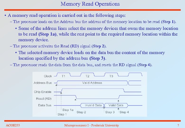 Memory Read Operations • A memory read operation is carried out in the following steps: – The processor loads on the Address bus the address of the memory location to be read (Step 1). • Some of the address lines select the memory devices that owns the memory location to be read (Step 1 a), while the rest point to the required memory location within the memory device. – The processor activates the Read (RD) signal (Step 2). • The selected memory device loads on the data bus the content of the memory location specified by the address bus (Step 3). – The processor reads the data from the data bus, and resets the RD signal (Step 4). ACOE 255 Microprocessors I - Frederick University 7
 Memory Write Operations • A memory write operation is carried out in the following steps: – The processor loads on the Address bus the address of the memory location (Step 1). • Some of the address lines select the memory devices that owns the memory location to be written (Step 1 a), while the rest point to the required memory location within the memory device. – The processor loads on the data bus the data to be written (Step 2). – The processor activates the Write (WR) signal (Step 3). • The data at the data bus is stored in the memory location specified by the address bus (Step 4). ACOE 255 Microprocessors I - Frederick University 8
 Types of Semiconductor Memory Devices • Read Only Memory (ROM) A memory device that maintains its data permanently (or until the device is reprogrammed). Random Access Memory (RAM) • A memory device that can be read and written. – – Non-volatile: It maintains its data even without power supply. • Used to store – Programs such as the BIOS. – Data such as look tables • e. g. the bit pattern of the characters in a dot matrix printer. • A ROM device can be 1. Masked ROM (Programmed by the manufacturer) 2. Programmable ROM (can be program-erased-reprogrammed many times ACOE 255 – • Used to store – – • Volatile: It looses its data when the power supply is switched-off When the supply is switched-on it contains random data User programs that are loaded from a secondary memory (disk) Temporary data used by programs such as variables and arrays. A RAM device can be 1. Static 2. dynamic Microprocessors I - Frederick University 9
 A Read Only Memory Example • Implementation of an 8 X 4 ROM using (a) a decoder and OR-gates and (b) a decoder and diodes. ACOE 255 Microprocessors I - Frederick University 10
 A Programmable Read Only Memory Example • Implementation of an 8 X 4 ROM using a decoder and fused links. ACOE 255 Microprocessors I - Frederick University 11
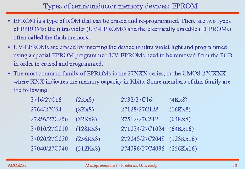 Types of semiconductor memory devices: EPROM • EPROM is a type of ROM that can be erased and re-programmed. There are two types of EPROMs: the ultra-violet (UV-EPROMs) and the electrically erasable (EEPROMs) often called the flash memory. • UV-EPROMs are erased by inserting the device in ultra violet light and programmed using a special EPROM programmer. UV-EPROMs need to be removed from the PCB in order to erased and programmed. • The most common family of EPROMs is the 27 XXX series, or the CMOS 27 CXXX where XXX indicates the memory capacity in Kbits. Some members of this family are the following: 2716/27 C 16 2732/27 C 16 (4 Kx 8) 2764/27 C 64 (8 Kx 8) 27128/27 C 128 (16 Kx 8) 27256/27 C 256 (32 Kx 8) 27512/27 C 512 (64 Kx 8) 27010/27 C 010 (128 Kx 8) 271024/27 C 1024 (64 Kx 16) 27020/27 C 020 (256 Kx 8) 272048/27 C 2048 (128 Kx 16) 27040/27 C 040 ACOE 255 (2 Kx 8) (512 Kx 8) 274096/27 C 4096 (256 Kx 16) Microprocessors I - Frederick University 12
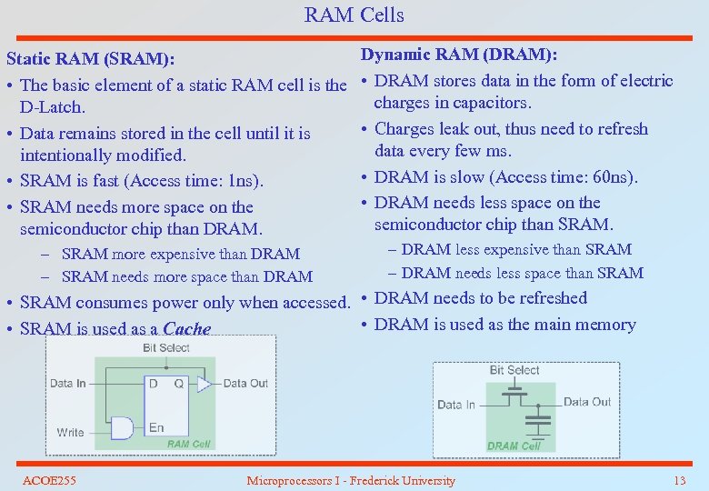 RAM Cells Static RAM (SRAM): • The basic element of a static RAM cell is the D-Latch. • Data remains stored in the cell until it is intentionally modified. • SRAM is fast (Access time: 1 ns). • SRAM needs more space on the semiconductor chip than DRAM. Dynamic RAM (DRAM): • DRAM stores data in the form of electric charges in capacitors. • Charges leak out, thus need to refresh data every few ms. • DRAM is slow (Access time: 60 ns). • DRAM needs less space on the semiconductor chip than SRAM. – SRAM more expensive than DRAM – SRAM needs more space than DRAM – DRAM less expensive than SRAM – DRAM needs less space than SRAM • SRAM consumes power only when accessed. • DRAM needs to be refreshed • DRAM is used as the main memory • SRAM is used as a Cache ACOE 255 Microprocessors I - Frederick University 13
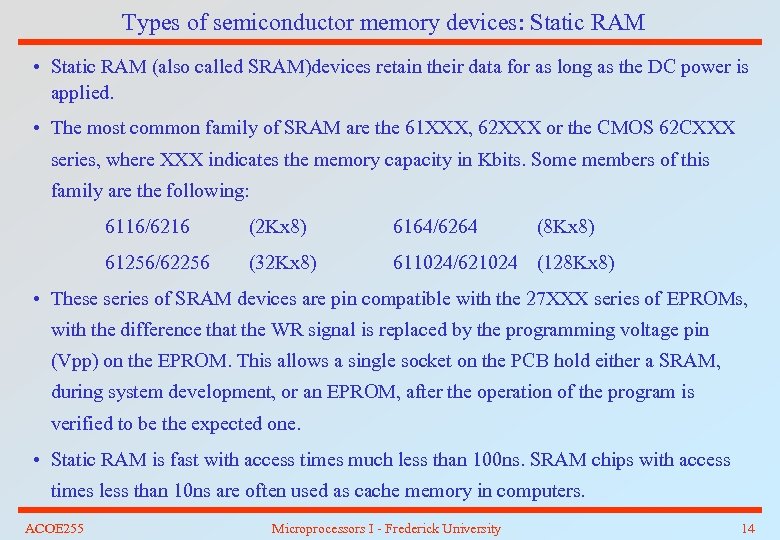 Types of semiconductor memory devices: Static RAM • Static RAM (also called SRAM)devices retain their data for as long as the DC power is applied. • The most common family of SRAM are the 61 XXX, 62 XXX or the CMOS 62 CXXX series, where XXX indicates the memory capacity in Kbits. Some members of this family are the following: 6116/6216 (2 Kx 8) 6164/6264 (8 Kx 8) 61256/62256 (32 Kx 8) 611024/621024 (128 Kx 8) • These series of SRAM devices are pin compatible with the 27 XXX series of EPROMs, with the difference that the WR signal is replaced by the programming voltage pin (Vpp) on the EPROM. This allows a single socket on the PCB hold either a SRAM, during system development, or an EPROM, after the operation of the program is verified to be the expected one. • Static RAM is fast with access times much less than 100 ns. SRAM chips with access times less than 10 ns are often used as cache memory in computers. ACOE 255 Microprocessors I - Frederick University 14
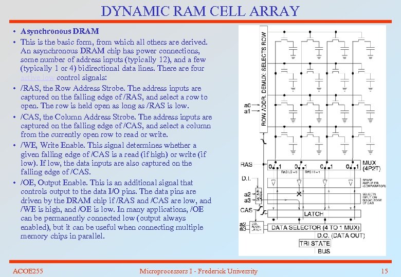 DYNAMIC RAM CELL ARRAY • Asynchronous DRAM • This is the basic form, from which all others are derived. An asynchronous DRAM chip has power connections, some number of address inputs (typically 12), and a few (typically 1 or 4) bidirectional data lines. There are four active low control signals: • /RAS, the Row Address Strobe. The address inputs are captured on the falling edge of /RAS, and select a row to open. The row is held open as long as /RAS is low. • /CAS, the Column Address Strobe. The address inputs are captured on the falling edge of /CAS, and select a column from the currently open row to read or write. • /WE, Write Enable. This signal determines whether a given falling edge of /CAS is a read (if high) or write (if low). If low, the data inputs are also captured on the falling edge of /CAS. • /OE, Output Enable. This is an additional signal that controls output to the data I/O pins. The data pins are driven by the DRAM chip if /RAS and /CAS are low, and /WE is high, and /OE is low. In many applications, /OE can be permanently connected low (output always enabled), but it can be useful when connecting multiple memory chips in parallel. ACOE 255 Microprocessors I - Frederick University 15
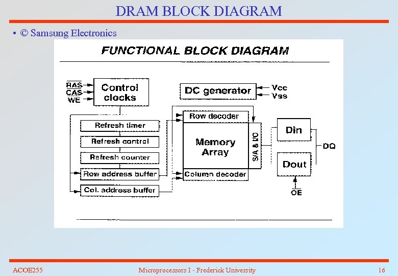 DRAM BLOCK DIAGRAM • © Samsung Electronics ACOE 255 Microprocessors I - Frederick University 16
 DYNAMIC RAM • DRAM requires refreshing every 2 to 4 ms. • Refreshing occurs automatically during a read or write. • Internal circuitry takes care of refreshing cells that are not accessed over this interval. – For a 256 K X 1 DRAM with 256 rows, a refresh must occur every 15. 6 us (4 ms/256). – For the 8086, a read or write occurs every 800 ns. – This allows 19 memory reads/writes per refresh or 5% of the time. • DRAM technologies – – EDO DRAM SDRAM DRDRAM DDR DRAM • Soft errors occur on DRAMs which often require ERROR DETECTION and/or ERROR CORRECTION • A DRAM CONTROLLER is required for using DRAM ACOE 255 Microprocessors I - Frederick University 17
 EXTENDED DATA OUTPUT (EDO) DRAM • Any memory access in an EDO memory (including a refresh) stores the 256 bits in a set of latches. • Any subsequent access to bytes in this set are immediately available (without the decode time and therefore wait states). • This works well because of the principle of spatial locality, and improves system performance by 15 to 25 % ! ACOE 255 Microprocessors I - Frederick University 18
 SYNCHRONOUS DYNAMIC RAM • In a synchronous DRAM, the control signals are synchronized with the system bus clock and therefore with the microprocessor • It allows pipelined read/write operations ACOE 255 Microprocessors I - Frederick University 19
 Double Data Rate (DDR) DRAM • An SDRAM type of memory where data are transferred on both the rising and the falling clock edge, effectively doubling the transfer rate without increasing the clock frequency • DDR-200 means a transfer rate of 200 million transfers per second, at a clock rate of 100 MHz • DDR 1 upto 400 MHz • DDR 2 standard allows higher clock frequencies ACOE 255 Microprocessors I - Frederick University 20
 Direct Rambus DRAM (DRDRAM) • A type of dual-edge SDRAM, like DDR, challenging DDR 2 as the standard ACOE 255 Microprocessors I - Frederick University 21
 ERRORS AND ERROR DETECTION AND CORRECTION • Electrical or magnetic interference inside a computer system as well as cosmic radiation cause a single bit of DRAM to spontaneously flip to the opposite state. (“soft“ errors) • As the components on DRAM chips get smaller while operating voltages continue to fall, DRAM chips may be: – affected by such radiation more frequently since lower energy particles will be able to change a memory cell's state. – or since smaller cells make smaller targets individual cells may be less susceptible to such effects • A reasonable rule of thumb is to expect one bit error, per month, per gigabyte of memory • Systems often use error detection and correction methods to identify and possibly correct soft errors – – repetition schemes parity schemes (74 AS 280) cyclic redundancy checks Hamming distance based checks (74 LS 636) ACOE 255 Microprocessors I - Frederick University 22
 ERROR DETECTION: PARITY • A parity bit is a bit added to a fixed number of data bits to ensure that the total number of ‘ 1’s is either odd (odd parity) or even (even parity) • Therefore, if the number of data bit ‘ 1’s is odd in an even parity scheme, the parity bit is ‘ 1’, otherwise it is ‘ 0’ • Likewise, if the number of data bit ‘ 1’s is even in an odd parity scheme, the parity bit is ‘ 1’, otherwise it is ‘ 0’ • The parity bit is transmitted with the data, and checked by the receiver • Advantages: – Only one bit overhead – Simple digital circuit implementation • Disadvantages: – Cannot correct errors, only detect them – Only detects an odd number of errors ACOE 255 Microprocessors I - Frederick University 23
 PARITY EXAMPLE • Calculate the parity bit for both even and odd parity, for the following sequence – – – 1001 0001 1000011 Assuming that the last bit is the parity bit (odd parity), determine which data transmission was successful and which unsuccessful – 10001010 – 00111011 – 1101 • Design the circuit that gives the parity bit ACOE 255 Microprocessors I - Frederick University 24
 ERROR CORRECTION: REPETITION AND MAJORITY VOTING • Data are saved (copied) in three different memory elements • During a memory read, all three memories are accessed and majority voting circuitry decides the final output. • Advantages: the possibility of soft errors is practically eliminated • Disadvantages: Triple(!) memory space is required, and there is a performance and area overhead caused by the majority voting circuitry ACOE 255 Microprocessors I - Frederick University 25
 EXAMPLE • Design the majority voting circuit for one memory bit ACOE 255 Microprocessors I - Frederick University 26
 DRAM CONTROLLER • A circuit performing address multiplexing and DRAM control signal generation ACOE 255 Microprocessors I - Frederick University 27
 Semiconductor Memory Expansion • The size of memory devices is usually less than the memory requirements of a computer system. • In all computers, more than one memory devices are combined together to form the main memory of the system. • Any computer must have at least one ROM chip and one RAM chip. • Word size memory expansion: – Most memory devices have a word size (number of data lines) of 8 or 16 bits. – The word size of today’s microprocessors is 32 bits (80386, 80486) or 64 bits (Pentium) • Address size memory expansion: – The size of common memory chips is usually less or in the order of 256 M-byte. – Most personal computers have more than 2 Gbytes of RAM. – Workstations and other high throughput computers have more than 4 Gbytes of RAM. ACOE 255 Microprocessors I - Frederick University 28
 Memory Expansion on Motherboards Memory Expansion Using 4 SIMMs on the Motherboard ACOE 255 Memory Expansion using 4 Memory Chips on a SIMM Microprocessors I - Frederick University 29
 Memory Address Size Expansion • More than one memory devices can be used to expand the number of memory locations on the system. • To expand the word size do the following: – Determine the number of memory chips required, by dividing the required memory size with the size of the memory devices to be used. – Connect the data lines of each memory chip in parallel on the data lines of the processor. – Connect the address lines of each memory chip in parallel with the low address lines of the processor. – Connect the CS lines of each memory device with the high address lines of the processor through an address decoding circuit. . – Connect together all WR and all RD lines of each memory device. ACOE 255 Microprocessors I - Frederick University 30
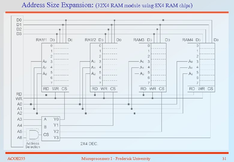 Address Size Expansion: (32 X 4 RAM module using 8 X 4 RAM chips) ACOE 255 Microprocessors I - Frederick University 31
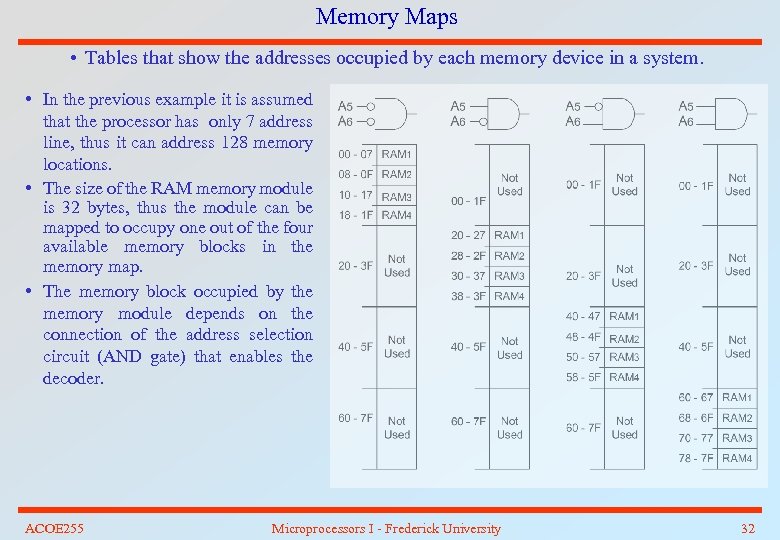 Memory Maps • Tables that show the addresses occupied by each memory device in a system. • In the previous example it is assumed that the processor has only 7 address line, thus it can address 128 memory locations. • The size of the RAM memory module is 32 bytes, thus the module can be mapped to occupy one out of the four available memory blocks in the memory map. • The memory block occupied by the memory module depends on the connection of the address selection circuit (AND gate) that enables the decoder. ACOE 255 Microprocessors I - Frederick University 32
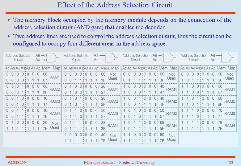 Effect of the Address Selection Circuit • The memory block occupied by the memory module depends on the connection of the address selection circuit (AND gate) that enables the decoder. • Two address lines are used to control the address selection circuit, thus the circuit can be configured to occupy four different areas in the address space. ACOE 255 Microprocessors I - Frederick University 33
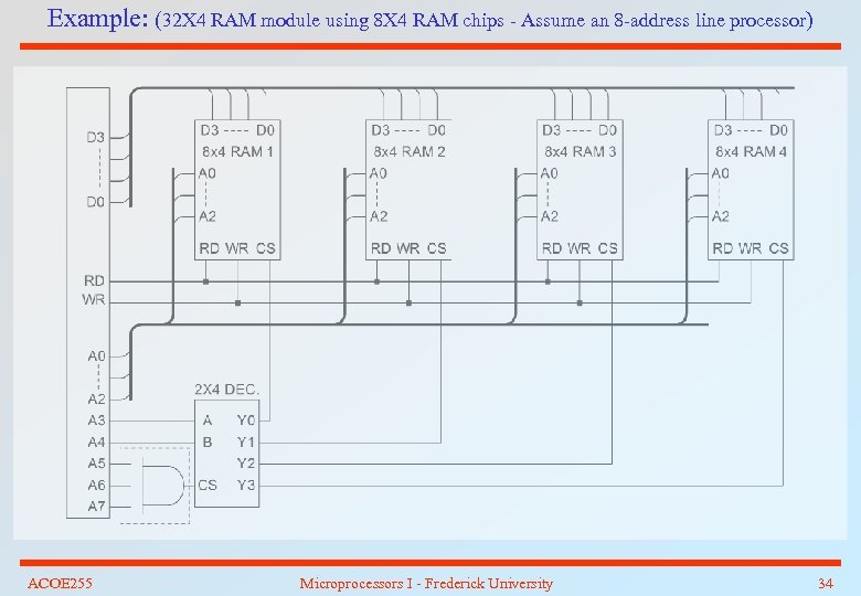 Example: (32 X 4 RAM module using 8 X 4 RAM chips - Assume an 8 -address line processor) ACOE 255 Microprocessors I - Frederick University 34
 Memory Map for previous example. • There are three address lines connected on the address selection circuit. Thus there can be eight different memory map configurations. • Three possible memory map configurations are shown below. ACOE 255 Microprocessors I - Frederick University 35
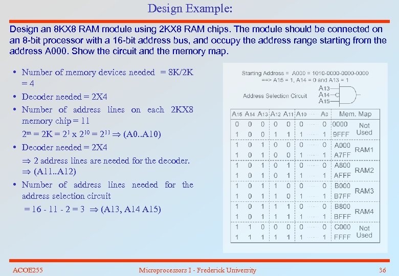 Design Example: Design an 8 KX 8 RAM module using 2 KX 8 RAM chips. The module should be connected on an 8 -bit processor with a 16 -bit address bus, and occupy the address range starting from the address A 000. Show the circuit and the memory map. • Number of memory devices needed = 8 K/2 K =4 • Decoder needed = 2 X 4 • Number of address lines on each 2 KX 8 memory chip = 11 2 m = 2 K = 21 x 210 = 211 (A 0. . A 10) • Decoder needed = 2 X 4 2 address lines are needed for the decoder. (A 11. . A 12) • Number of address lines needed for the address selection circuit = 16 - 11 - 2 = 3 (A 13, A 14 A 15) ACOE 255 Microprocessors I - Frederick University 36
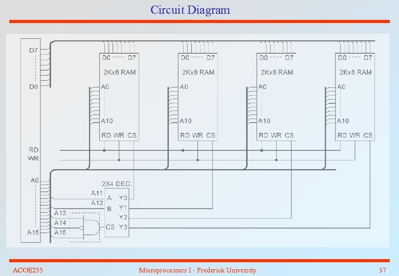 Circuit Diagram ACOE 255 Microprocessors I - Frederick University 37
 Address Decoding • The physical address space, or memory map, of a microprocessor refers to the range of addresses of memory location that can accessed by the microprocessor. The size of the address space depends on the number of address lines of the microprocessor. • At least two memory devices are required in a microprocessor system: one for the ROM and one for the RAM. • In an 8088/8086 the high addresses in the memory map should always be occupied by a ROM, while the low addresses in the memory map should always be occupied by a RAM. • Address decoding is required in order to enable the connection of more than one memory devices on the microprocessor. Each device will occupy a unique area in the memory map. • A memory system is not fully decoded if some of the address lines are not used by the address decoding circuit or memory. In this case a memory device will occupy more than one sections in the memory map. This is referred as memory mirroring or memory imaging. ACOE 255 Microprocessors I - Frederick University 38
 Address Decoding Circuits • A number of types of address decoding circuits can be used in a microprocessor system. The main issues related to the selection of an address decoding circuit are: – The time delays introduced by the address decoding circuit. This delays are added to the access time of the memory devices, and might yield to the insertion of wait states. – The number of chips required by the address decoding circuit, as well as the complexity of the circuit (number of tracks required on the board. • An address decoding circuit must ensure that an address section is occupied by only one memory device. If two or more devices occupy the same addresses then bus contention will occur. Bus contention occurs if two of more devices drive the bus at the same time. Bus contention can be either static or dynamic. – Static bus contention occurs when two or more devices drive a bus for a prolonged time period. This might damage some of the components of the system. Static bus contention might be caused by improper address decoding design, or by other faults in the system such as a short circuit of the CS of a device to the ground. – Dynamic bus contention occurs when two or more devices drive a bus for a short period of time. This might change the logic levels on the bus and cause system malfunctions. Dynamic bus contention might be caused by improper address decoding design, or by wrong memory timing analysis. ACOE 255 Microprocessors I - Frederick University 39
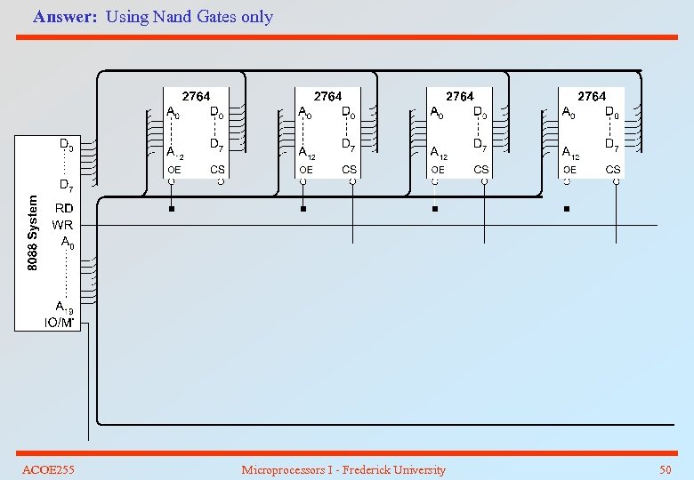
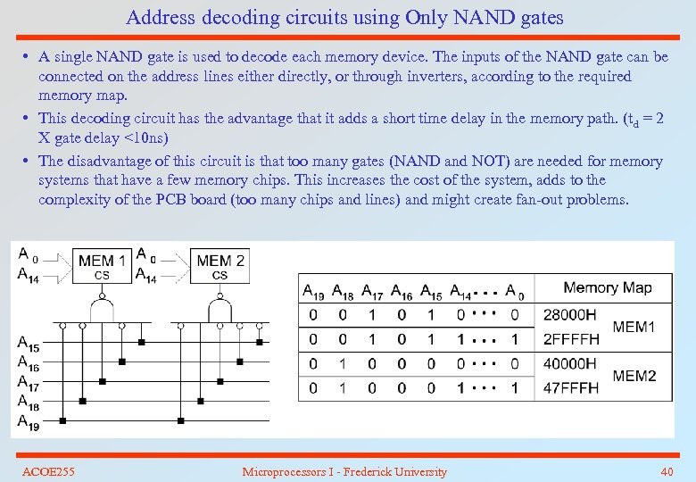 Address decoding circuits using Only NAND gates • A single NAND gate is used to decode each memory device. The inputs of the NAND gate can be connected on the address lines either directly, or through inverters, according to the required memory map. • This decoding circuit has the advantage that it adds a short time delay in the memory path. (t d = 2 X gate delay <10 ns) • The disadvantage of this circuit is that too many gates (NAND and NOT) are needed for memory systems that have a few memory chips. This increases the cost of the system, adds to the complexity of the PCB board (too many chips and lines) and might create fan-out problems. ACOE 255 Microprocessors I - Frederick University 40
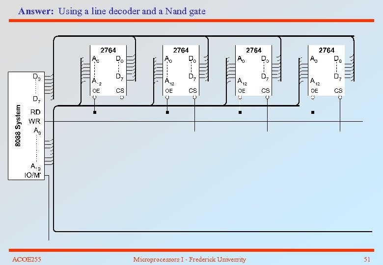
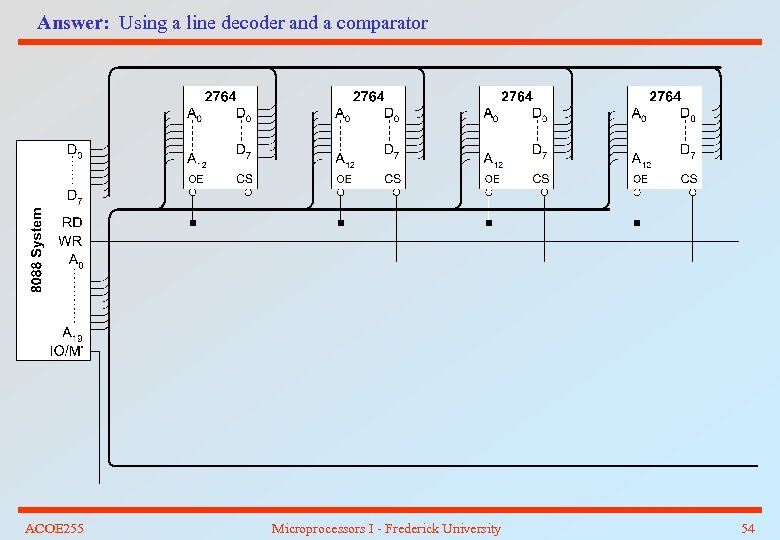
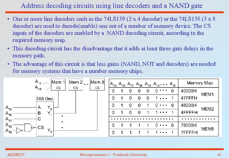 Address decoding circuits using line decoders and a NAND gate • One or more line decoders such as the 74 LS 139 (2 x 4 decoder) or the 74 LS 138 (3 x 8 decoder) are used to decode(enable) one out of a number of memory device. The CS inputs of the decoders are enabled by a NAND decoding circuit, according to the required memory map. • This decoding circuit has the disadvantage that it adds at least three gate delays in the memory path. • The advantage of this circuit is that less gates (NAND, NOT and decoders) are needed for memory systems that have a number memory chips. ACOE 255 Microprocessors I - Frederick University 41
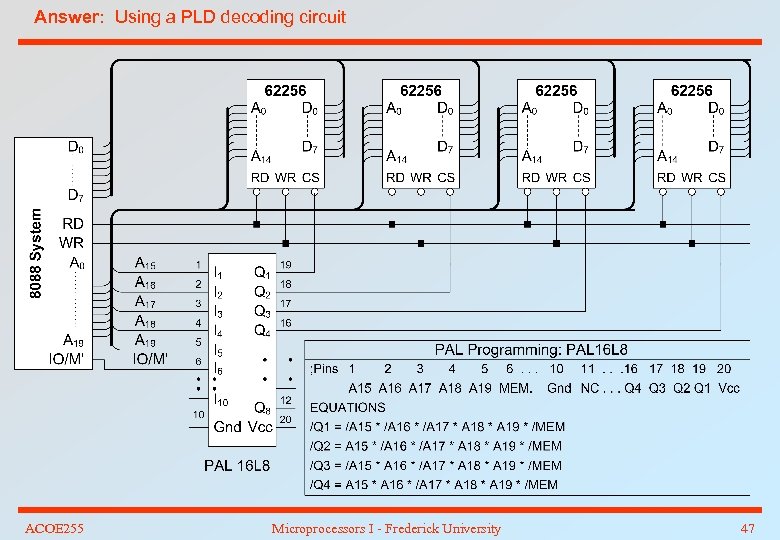
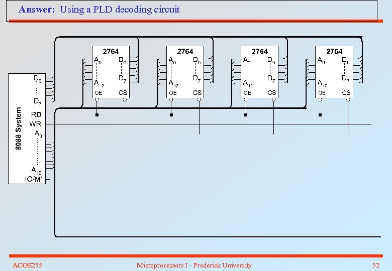
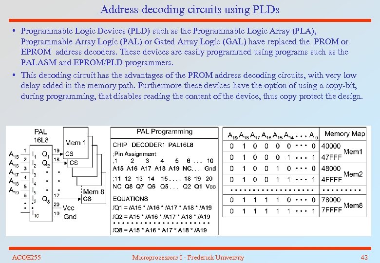 Address decoding circuits using PLDs • Programmable Logic Devices (PLD) such as the Programmable Logic Array (PLA), Programmable Array Logic (PAL) or Gated Array Logic (GAL) have replaced the PROM or EPROM address decoders. These devices are easily programmed using programs such as the PALASM and EPROM/PLD programmers. • This decoding circuit has the advantages of the PROM address decoding circuits, with very low delay added in the memory path. Furthermore these devices have the option of using a copy-bit, during programming, that disables reading the content of the device, thus copy protect the design. ACOE 255 Microprocessors I - Frederick University 42
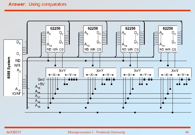
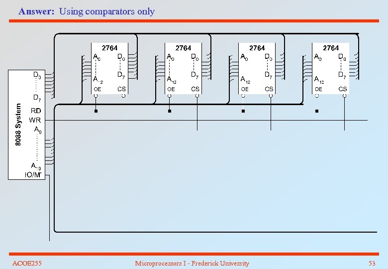
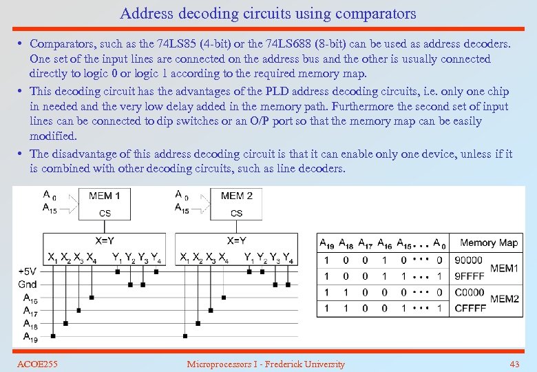 Address decoding circuits using comparators • Comparators, such as the 74 LS 85 (4 -bit) or the 74 LS 688 (8 -bit) can be used as address decoders. One set of the input lines are connected on the address bus and the other is usually connected directly to logic 0 or logic 1 according to the required memory map. • This decoding circuit has the advantages of the PLD address decoding circuits, i. e. only one chip in needed and the very low delay added in the memory path. Furthermore the second set of input lines can be connected to dip switches or an O/P port so that the memory map can be easily modified. • The disadvantage of this address decoding circuit is that it can enable only one device, unless if it is combined with other decoding circuits, such as line decoders. ACOE 255 Microprocessors I - Frederick University 43
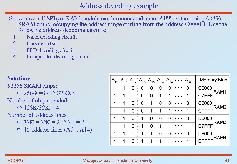 Address decoding example Show a 128 Kbyte RAM module can be connected on an 8088 system using 62256 SRAM chips, occupying the address range starting from the address C 0000 H. Use the following address decoding circuits: 1 2 3 4. Nand decoding circuits Line decoders PLD decoding circuit Comparator decoding circuit Solution: 62256 SRAM chips: 256/8 =32 32 KX 8 Number of chips needed: 128 K/32 K = 4 Number of address lines: 32 K = 25 * 210 = 215 15 address lines (A 0. . A 14) ACOE 255 Microprocessors I - Frederick University 44
 Answer: Using NAND gates ACOE 255 Microprocessors I - Frederick University 45
 Answer: Using a line decoder and a NAND gate ACOE 255 Microprocessors I - Frederick University 46
 Answer: Using a PLD decoding circuit ACOE 255 Microprocessors I - Frederick University 47
 Answer: Using comparators ACOE 255 Microprocessors I - Frederick University 48
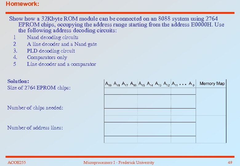 Homework: Show a 32 Kbyte ROM module can be connected on an 8088 system using 2764 EPROM chips, occupying the address range starting from the address E 0000 H. Use the following address decoding circuits: 1 2 3. 4. 5 Nand decoding circuits A line decoder and a Nand gate PLD decoding circuit Comparators only Line decoder and a comparator Solution: Size of 2764 EPROM chips: Number of chips needed: Number of address lines: ACOE 255 Microprocessors I - Frederick University 49
 Answer: Using Nand Gates only ACOE 255 Microprocessors I - Frederick University 50
 Answer: Using a line decoder and a Nand gate ACOE 255 Microprocessors I - Frederick University 51
 Answer: Using a PLD decoding circuit ACOE 255 Microprocessors I - Frederick University 52
 Answer: Using comparators only ACOE 255 Microprocessors I - Frederick University 53
 Answer: Using a line decoder and a comparator ACOE 255 Microprocessors I - Frederick University 54
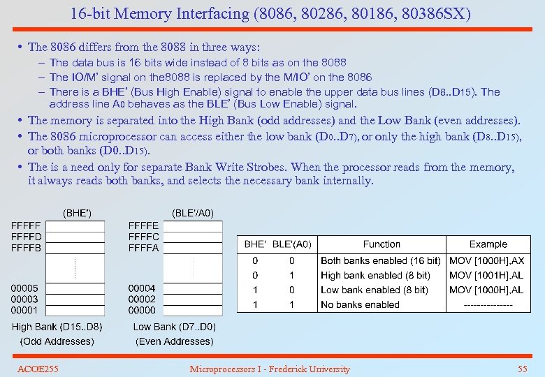 16 -bit Memory Interfacing (8086, 80286, 80186, 80386 SX) • The 8086 differs from the 8088 in three ways: – The data bus is 16 bits wide instead of 8 bits as on the 8088 – The IO/M’ signal on the 8088 is replaced by the M/IO’ on the 8086 – There is a BHE’ (Bus High Enable) signal to enable the upper data bus lines (D 8. . D 15). The address line A 0 behaves as the BLE’ (Bus Low Enable) signal. • The memory is separated into the High Bank (odd addresses) and the Low Bank (even addresses). • The 8086 microprocessor can access either the low bank (D 0. . D 7), or only the high bank (D 8. . D 15), or both banks (D 0. . D 15). • The is a need only for separate Bank Write Strobes. When the processor reads from the memory, it always reads both banks, and selects the necessary bank internally. ACOE 255 Microprocessors I - Frederick University 55
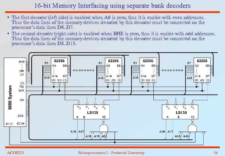 16 -bit Memory Interfacing using separate bank decoders • The first decoder (left side) is enabled when A 0 is zero, thus it is enable with even addresses. Thus the data lines of the memory devices decoded by this decoder must be connected on the processor’s data lines D 0. . D 7. • The second decoder (right side) is enabled when BHE is zero, thus it is enable with odd addresses. Thus the data lines of the memory devices decoded by this decoder must be connected on the processor’s data lines D 8. . D 15. ACOE 255 Microprocessors I - Frederick University 56
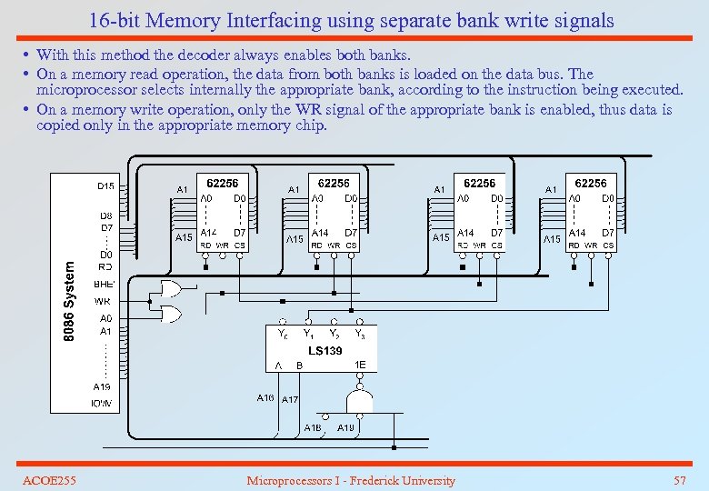 16 -bit Memory Interfacing using separate bank write signals • With this method the decoder always enables both banks. • On a memory read operation, the data from both banks is loaded on the data bus. The microprocessor selects internally the appropriate bank, according to the instruction being executed. • On a memory write operation, only the WR signal of the appropriate bank is enabled, thus data is copied only in the appropriate memory chip. ACOE 255 Microprocessors I - Frederick University 57
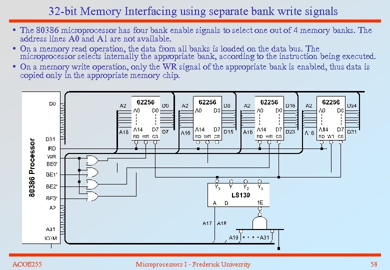 32 -bit Memory Interfacing using separate bank write signals • The 80386 microprocessor has four bank enable signals to select one out of 4 memory banks. The address lines A 0 and A 1 are not available. • On a memory read operation, the data from all banks is loaded on the data bus. The microprocessor selects internally the appropriate bank, according to the instruction being executed. • On a memory write operation, only the WR signal of the appropriate bank is enabled, thus data is copied only in the appropriate memory chip. ACOE 255 Microprocessors I - Frederick University 58
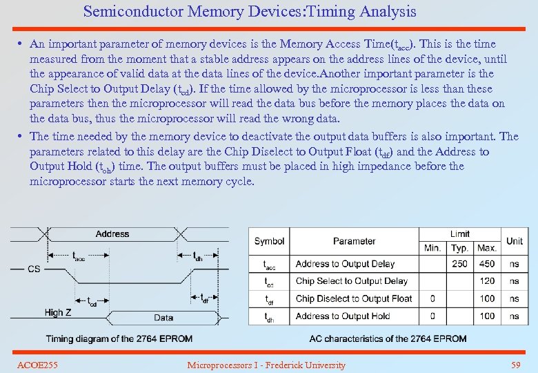 Semiconductor Memory Devices: Timing Analysis • An important parameter of memory devices is the Memory Access Time(tacc). This is the time measured from the moment that a stable address appears on the address lines of the device, until the appearance of valid data at the data lines of the device. Another important parameter is the Chip Select to Output Delay (tcd). If the time allowed by the microprocessor is less than these parameters then the microprocessor will read the data bus before the memory places the data on the data bus, thus the microprocessor will read the wrong data. • The time needed by the memory device to deactivate the output data buffers is also important. The parameters related to this delay are the Chip Diselect to Output Float (tdf) and the Address to Output Hold (toh) time. The output buffers must be placed in high impedance before the microprocessor starts the next memory cycle. ACOE 255 Microprocessors I - Frederick University 59
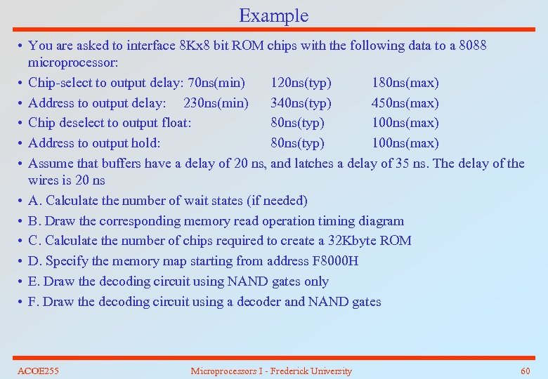 Example • You are asked to interface 8 Kx 8 bit ROM chips with the following data to a 8088 microprocessor: • Chip-select to output delay: 70 ns(min) 120 ns(typ) 180 ns(max) • Address to output delay: 230 ns(min) 340 ns(typ) 450 ns(max) • Chip deselect to output float: 80 ns(typ) 100 ns(max) • Address to output hold: 80 ns(typ) 100 ns(max) • Assume that buffers have a delay of 20 ns, and latches a delay of 35 ns. The delay of the wires is 20 ns • A. Calculate the number of wait states (if needed) • B. Draw the corresponding memory read operation timing diagram • C. Calculate the number of chips required to create a 32 Kbyte ROM • D. Specify the memory map starting from address F 8000 H • E. Draw the decoding circuit using NAND gates only • F. Draw the decoding circuit using a decoder and NAND gates ACOE 255 Microprocessors I - Frederick University 60


