a131d4dd3af3babae992ce7d036cdac9.ppt
- Количество слайдов: 100
 ME 1000 RF CIRCUIT DESIGN This courseware product contains scholarly and technical information and is protected by copyright laws and international treaties. No part of this publication may be reproduced by any means, be it transmitted, transcribed, photocopied, stored in a retrieval system, or translated into any language in any form, without the prior written permission of Acehub Vista Sdn. Bhd. or their respective copyright owners. The use of the courseware product and all other products developed and/or distributed by Acehub Vista Sdn. Bhd. are subject to the applicable License Agreement. For further information, see the Courseware Product License Agreement. http: //dreamcatcher. asia/cw 1
 10. RF Oscillators 2
![Main References • • [1]* D. M. Pozar, “Microwave engineering”, 2 nd Edition, 1998 Main References • • [1]* D. M. Pozar, “Microwave engineering”, 2 nd Edition, 1998](https://present5.com/presentation/a131d4dd3af3babae992ce7d036cdac9/image-3.jpg) Main References • • [1]* D. M. Pozar, “Microwave engineering”, 2 nd Edition, 1998 John-Wiley & Sons. [2] J. Millman, C. C. Halkias, “Integrated electronics”, 1972, Mc. Graw-Hill. [3] R. Ludwig, P. Bretchko, “RF circuit design - theory and applications”, 2000 Prentice-Hall. [4] B. Razavi, “RF microelectronics”, 1998 Prentice-Hall, TK 6560. [5] J. R. Smith, ”Modern communication circuits”, 1998 Mc. Graw-Hill. [6] P. H. Young, “Electronics communication techniques”, 5 th edition, 2004 Prentice-Hall. [7] Gilmore R. , Besser L. , ”Practical RF circuit design for modern wireless systems”, Vol. 1 & 2, 2003, Artech House. [8] Ogata K. , “Modern control engineering”, 4 th edition, 2005, Prentice-Hall. 3
Main References • • [1]* D. M. Pozar, “Microwave engineering”, 2 nd Edition, 1998 John-Wiley & Sons. [2] J. Millman, C. C. Halkias, “Integrated electronics”, 1972, Mc. Graw-Hill. [3] R. Ludwig, P. Bretchko, “RF circuit design - theory and applications”, 2000 Prentice-Hall. [4] B. Razavi, “RF microelectronics”, 1998 Prentice-Hall, TK 6560. [5] J. R. Smith, ”Modern communication circuits”, 1998 Mc. Graw-Hill. [6] P. H. Young, “Electronics communication techniques”, 5 th edition, 2004 Prentice-Hall. [7] Gilmore R. , Besser L. , ”Practical RF circuit design for modern wireless systems”, Vol. 1 & 2, 2003, Artech House. [8] Ogata K. , “Modern control engineering”, 4 th edition, 2005, Prentice-Hall. 3
 Agenda • Positive feedback oscillator concepts. • Negative resistance oscillator concepts (typically employed for RF oscillator). • Equivalence between positive feedback and negative resistance oscillator theory. • Oscillator start-up requirement and transient. • Oscillator design - Making an amplifier circuit unstable. • Constant | 1| circle. • Fixed frequency oscillator design. • Voltage-controlled oscillator design. 4
 1. 0 Oscillation Concepts 5
 Introduction • Oscillators are a class of circuits with 1 terminal or port, which produce a periodic electrical output upon power up. • Most of us would have encountered oscillator circuits while studying for our basic electronics classes. • Oscillators can be classified into two types: (A) Relaxation and (B) Harmonic oscillators. • Relaxation oscillators (also called astable multivibrator), is a class of circuits with two unstable states. The circuit switches back-and-forth between these states. The output is generally square waves. • Harmonic oscillators are capable of producing near sinusoidal output, and is based on positive feedback approach. • Here we will focus on Harmonic Oscillators for RF systems. Harmonic oscillators are used as this class of circuits are capable of producing stable sinusoidal waveform with low phase noise. 6
 2. 0 Overview of Feedback Oscillators 7
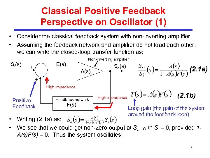 Classical Positive Feedback Perspective on Oscillator (1) • Consider the classical feedback system with non-inverting amplifier, • Assuming the feedback network and amplifier do not load each other, we can write the closed-loop transfer function as: Si(s) Non-inverting amplifier E(s) + A(s) So(s) (2. 1 a) + High impedance Positive Feedback network F(s) High impedance (2. 1 b) Loop gain (the gain of the system around the feedback loop) • Writing (2. 1 a) as: • We see that we could get non-zero output at So, with Si = 0, provided 1 A(s)F(s) = 0. Thus the system oscillates! 8
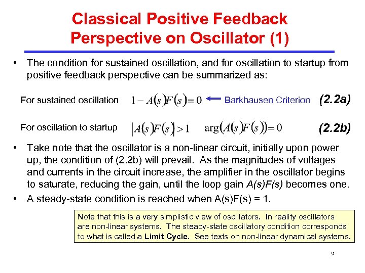 Classical Positive Feedback Perspective on Oscillator (1) • The condition for sustained oscillation, and for oscillation to startup from positive feedback perspective can be summarized as: For sustained oscillation For oscillation to startup Barkhausen Criterion (2. 2 a) (2. 2 b) • Take note that the oscillator is a non-linear circuit, initially upon power up, the condition of (2. 2 b) will prevail. As the magnitudes of voltages and currents in the circuit increase, the amplifier in the oscillator begins to saturate, reducing the gain, until the loop gain A(s)F(s) becomes one. • A steady-state condition is reached when A(s)F(s) = 1. Note that this is a very simplistic view of oscillators. In reality oscillators are non-linear systems. The steady-state oscillatory condition corresponds to what is called a Limit Cycle. See texts on non-linear dynamical systems. 9
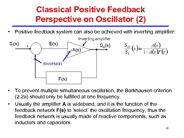 Classical Positive Feedback Perspective on Oscillator (2) • Positive feedback system can also be achieved with inverting amplifier: Inverting amplifier Si(s) E(s) + -A(s) So(s) - Inversion F(s) • To prevent multiple simultaneous oscillation, the Barkhausen criterion (2. 2 a) should only be fulfilled at one frequency. • Usually the amplifier A is wideband, and it is the function of the feedback network F(s) to ‘select’ the oscillation frequency, thus the feedback network is usually made of reactive components, such as inductors and capacitors. 10
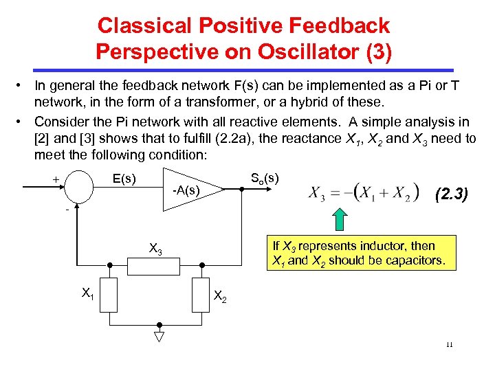 Classical Positive Feedback Perspective on Oscillator (3) • In general the feedback network F(s) can be implemented as a Pi or T network, in the form of a transformer, or a hybrid of these. • Consider the Pi network with all reactive elements. A simple analysis in [2] and [3] shows that to fulfill (2. 2 a), the reactance X 1, X 2 and X 3 need to meet the following condition: E(s) + So(s) -A(s) (2. 3) - If X 3 represents inductor, then X 1 and X 2 should be capacitors. X 3 X 1 X 2 11
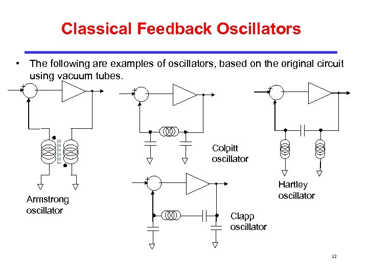 Classical Feedback Oscillators • The following are examples of oscillators, based on the original circuit using vacuum tubes. + + + - - - Colpitt oscillator + Armstrong oscillator Hartley oscillator - Clapp oscillator 12
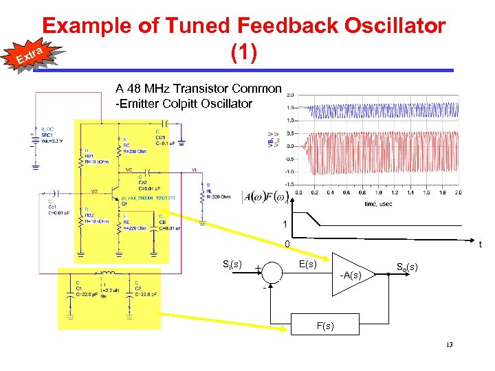 Example of Tuned Feedback Oscillator tra (1) Ex A 48 MHz Transistor Common -Emitter Colpitt Oscillator 1 0 Si(s) t E(s) + -A(s) So(s) F(s) 13
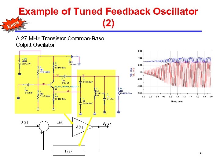 Example of Tuned Feedback Oscillator tra (2) Ex A 27 MHz Transistor Common-Base Colpitt Oscilator Si(s) E(s) + A(s) So(s) + F(s) 14
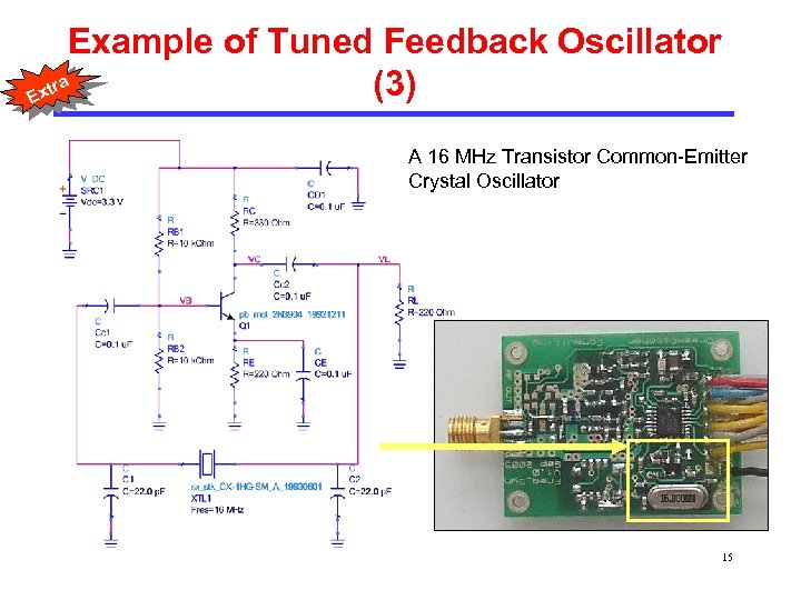 Example of Tuned Feedback Oscillator tra (3) Ex A 16 MHz Transistor Common-Emitter Crystal Oscillator 15
 Limitation of Feedback Oscillator • At high frequency, the assumption that the amplifier and feedback network do not load each other is not valid. In general the amplifier’s input impedance decreases with frequency, and it’s output impedance is not zero. Thus the actual loop gain is not A(s)F(s) and equation (2. 2) breakdowns. • Determining the loop gain of the feedback oscillator is cumbersome at high frequency. Moreover there could be multiple feedback paths due to parasitic inductance and capacitance. • It can be difficult to distinguish between the amplifier and the feedback paths, owing to the coupling between components and conductive structures on the printed circuit board (PCB) or substrate. • Generally it is difficult to physically implement a feedback oscillator once the operating frequency is higher than 500 MHz. 16
 3. 0 Negative Resistance Oscillators 17
 Introduction (1) • An alternative approach is needed to get a circuit to oscillate reliably. • We can view an oscillator as an amplifier that produces an output when there is no input. • Thus it is an unstable amplifier that becomes an oscillator! • For example let’s consider a conditionally stable amplifier. • Here instead of choosing load or source impedance in the stable regions of the Smith Chart, we purposely choose the load or source impedance in the unstable impedance regions. This will result in either | 1 | > 1 or | 2 | > 1. • The resulting amplifier circuit will be called the Destabilized Amplifier. • As seen in Chapter 7, having a reflection coefficient magnitude for 1 or 2 greater than one implies the corresponding port resistance R 1 or R 2 is negative, hence the name for this type of oscillator. 18
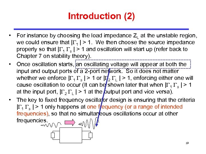 Introduction (2) • For instance by choosing the load impedance ZL at the unstable region, we could ensure that | 1 | > 1. We then choose the source impedance properly so that | 1 s | > 1 and oscillation will start up (refer back to Chapter 7 on stability theory). • Once oscillation starts, an oscillating voltage will appear at both the input and output ports of a 2 -port network. So it does not matter whether we enforce | 1 s | > 1 or | 2 L | > 1, enforcing either one will cause oscillation to occur (It can be shown later that when | 1 s | > 1 at the input port, | 2 L | > 1 at the output port and vice versa). • The key to fixed frequency oscillator design is ensuring that the criteria | 1 s | > 1 only happens at one frequency (or a range of intended frequencies), so that no simultaneous oscillations occur at other frequencies. 19
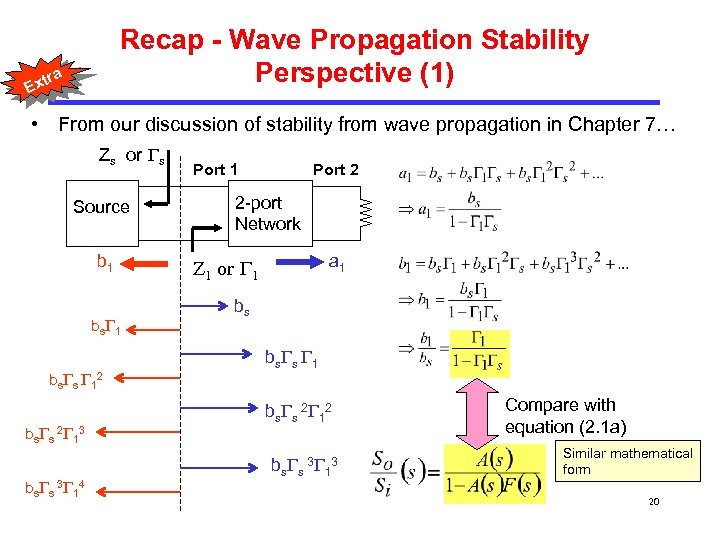 Recap - Wave Propagation Stability Perspective (1) tra Ex • From our discussion of stability from wave propagation in Chapter 7… Zs or s Source b 1 bs s 12 bs s 2 13 bs s 3 14 Port 1 Port 2 2 -port Network a 1 Z 1 or 1 bs b s s 1 b s s 2 1 2 b s s 3 1 3 Compare with equation (2. 1 a) Similar mathematical form 20
 tra Ex Recap - Wave Propagation Stability Perspective (2) • We see that the infinite series that constitute the steady-state incident (a 1) and reflected (b 1) waves at Port 1 will only converge provided | s 1| < 1. • These sinusoidal waves correspond to the voltage and current at the Port 1. If the waves are unbounded it means the corresponding sinusoidal voltage and current at the Port 1 will grow larger as time progresses, indicating oscillation start-up condition. • Therefore oscillation will occur when | s 1 | > 1. • Similar argument can be applied to port 2 since the signals at Port 1 and 2 are related to each other in a two-port network, and we see that the condition for oscillation at Port 2 is | L 2 | > 1. 21
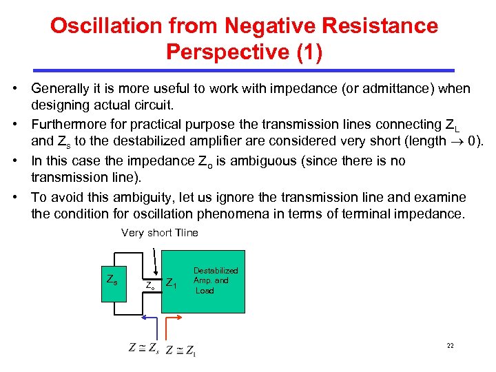 Oscillation from Negative Resistance Perspective (1) • Generally it is more useful to work with impedance (or admittance) when designing actual circuit. • Furthermore for practical purpose the transmission lines connecting ZL and Zs to the destabilized amplifier are considered very short (length 0). • In this case the impedance Zo is ambiguous (since there is no transmission line). • To avoid this ambiguity, let us ignore the transmission line and examine the condition for oscillation phenomena in terms of terminal impedance. Very short Tline Zs Zo Z 1 Destabilized Amp. and Load 22
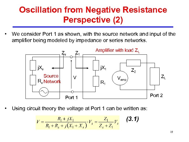 Oscillation from Negative Resistance Perspective (2) • We consider Port 1 as shown, with the source network and input of the amplifier being modeled by impedance or series networks. Zs Z 1 j. Xs Source Rs Network Amplifier with load ZL j. X 1 V R 1 Z 2 Vamp ZL Port 2 Port 1 • Using circuit theory the voltage at Port 1 can be written as: (3. 1) 23
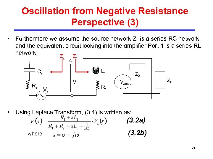 Oscillation from Negative Resistance Perspective (3) • Furthermore we assume the source network Zs is a series RC network and the equivalent circuit looking into the amplifier Port 1 is a series RL network. Zs Z 1 L 1 Cs Rs V Vs R 1 Z 2 Vamp ZL • Using Laplace Transform, (3. 1) is written as: (3. 2 a) where (3. 2 b) 24
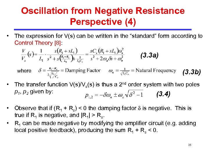 Oscillation from Negative Resistance Perspective (4) • The expression for V(s) can be written in the “standard” form according to Control Theory [8]: (3. 3 a) where (3. 3 b) • The transfer function V(s)/Vs(s) is thus a 2 nd order system with two poles p 1, p 2 given by: (3. 4) • Observe that if (R 1 + Rs) < 0 the damping factor is negative. This is true if R 1 is negative, and |R 1| > Rs. • R 1 can be made negative by modifying the amplifier circuit (e. g. adding local positive feedback), producing the sum R 1 + Rs < 0. 25
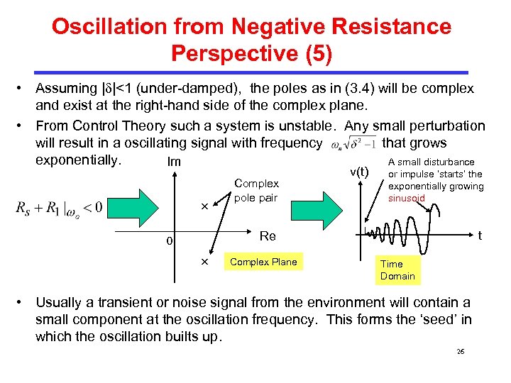 Oscillation from Negative Resistance Perspective (5) • Assuming | |<1 (under-damped), the poles as in (3. 4) will be complex and exist at the right-hand side of the complex plane. • From Control Theory such a system is unstable. Any small perturbation will result in a oscillating signal with frequency that grows exponentially. A small disturbance Im Complex pole pair v(t) or impulse ‘starts’ the exponentially growing sinusoid t Re 0 Complex Plane Time Domain • Usually a transient or noise signal from the environment will contain a small component at the oscillation frequency. This forms the ‘seed’ in which the oscillation builts up. 26
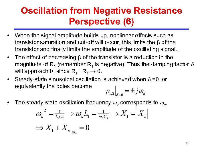 Oscillation from Negative Resistance Perspective (6) • When the signal amplitude builds up, nonlinear effects such as transistor saturation and cut-off will occur, this limits the of the transistor and finally limits the amplitude of the oscillating signal. • The effect of decreasing of the transistor is a reduction in the magnitude of R 1 (remember R 1 is negative). Thus the damping factor will approach 0, since Rs+ R 1 0. • Steady-state sinusoidal oscillation is achieved when =0, or equivalently the poles become • The steady-state oscillation frequency o corresponds to n, 27
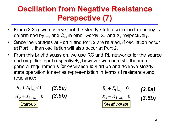 Oscillation from Negative Resistance Perspective (7) • From (3. 3 b), we observe that the steady-state oscillation frequency is determined by L 1 and Cs, in other words, X 1 and Xs respectively. • Since the voltages at Port 1 and Port 2 are related, if oscillation occur at Port 1, then oscillation will also occur at Port 2. • From this brief discussion, we use RC and RL networks for the source and amplifier input respectively, however we can distill the more general requirements for oscillation to start-up and achieve steadystate operation for series representation in terms of resistance and reactance: (3. 5 a) (3. 5 b) Start-up (3. 6 a) (3. 6 b) Steady-state 28
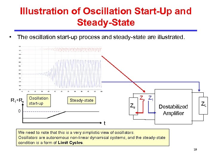 Illustration of Oscillation Start-Up and Steady-State • The oscillation start-up process and steady-state are illustrated. R 1+Rs Oscillation start-up Zs Z 1 Steady-state Zs 0 ZL Destabilized Amplifier t We need to note that this is a very simplistic view of oscillators. Oscillators are autonomous non-linear dynamical systems, and the steady-state condition is a form of Limit Cycles. 29
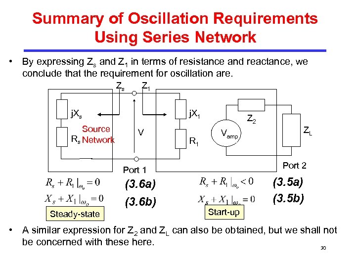 Summary of Oscillation Requirements Using Series Network • By expressing Zs and Z 1 in terms of resistance and reactance, we conclude that the requirement for oscillation are. Zs Z 1 j. Xs Source Rs Network j. X 1 V R 1 Z 2 Vamp Port 2 Port 1 (3. 6 a) (3. 6 b) Steady-state ZL (3. 5 a) (3. 5 b) Start-up • A similar expression for Z 2 and ZL can also be obtained, but we shall not be concerned with these here. 30
 The Resonator • The source network Zs is usually called the Resonator, as it is clear that equations (3. 5 b) and (3. 6 b) represent the resonance condition between the source network and the amplifier input. • The design of the resonator is extremely important. • We shall see later that an important parameter of the oscillator, the Phase Noise is dependent on the quality of the resonator. 31
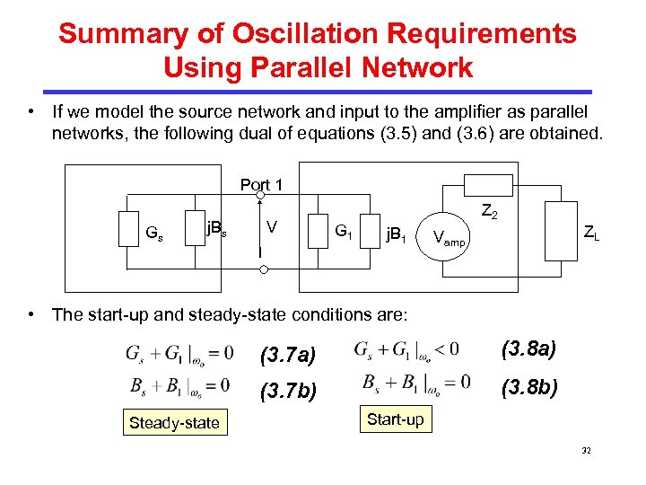 Summary of Oscillation Requirements Using Parallel Network • If we model the source network and input to the amplifier as parallel networks, the following dual of equations (3. 5) and (3. 6) are obtained. Port 1 Gs j. Bs V G 1 Z 2 j. B 1 ZL Vamp • The start-up and steady-state conditions are: (3. 7 a) (3. 7 b) Steady-state (3. 8 a) (3. 8 b) Start-up 32
 Series or Parallel Representation? (1) • The question is which to use? Series or parallel network representation? This is not an easy question to answer as the destabilized amplifier is operating in nonlinear region as oscillator. • Concept of impedance is not valid and our discussion is only an approximation at best. • We can assume series representation, and worked out the corresponding resonator impedance. If after computer simulation we discover that the actual oscillating frequency is far from our prediction (if there’s any oscillation at all!), then it probably means that the series representation is incorrect, and we should try the parallel representation. • Another clue to whether series or parallel representation is more accurate is to observe the current and voltage in the resonator. For series circuit the current is near sinusoidal, where as for parallel circuit it is the voltage that is sinusoidal. 33
![Series or Parallel Representation? (2) • Reference [7] illustrates another effective alternative, by computing Series or Parallel Representation? (2) • Reference [7] illustrates another effective alternative, by computing](https://present5.com/presentation/a131d4dd3af3babae992ce7d036cdac9/image-34.jpg) Series or Parallel Representation? (2) • Reference [7] illustrates another effective alternative, by computing the large-signal S 11 of Port 1 (with respect to Zo) using CAD software. • 1/S 11 is then plotted on a Smith Chart as a function of input signal magnitude at the operating frequency. • By comparing the locus of 1/S 11 as input signal magnitude is gradually increased with the coordinate of constant X or constant B circles on the Smith Chart, we can decide whether series or parallel form approximates Port 1 best. • We will adopt this approach, but plot S 11 instead of 1/S 11. This will be illustrated in the examples in next section. • Do note that there are other reasons that can cause the actual oscillation frequency to deviate a lot from prediction, such as frequency stability issue (see [1] and [7]). 34
Series or Parallel Representation? (2) • Reference [7] illustrates another effective alternative, by computing the large-signal S 11 of Port 1 (with respect to Zo) using CAD software. • 1/S 11 is then plotted on a Smith Chart as a function of input signal magnitude at the operating frequency. • By comparing the locus of 1/S 11 as input signal magnitude is gradually increased with the coordinate of constant X or constant B circles on the Smith Chart, we can decide whether series or parallel form approximates Port 1 best. • We will adopt this approach, but plot S 11 instead of 1/S 11. This will be illustrated in the examples in next section. • Do note that there are other reasons that can cause the actual oscillation frequency to deviate a lot from prediction, such as frequency stability issue (see [1] and [7]). 34
 4. 0 Fixed Frequency Negative Resistance Oscillator Design 35
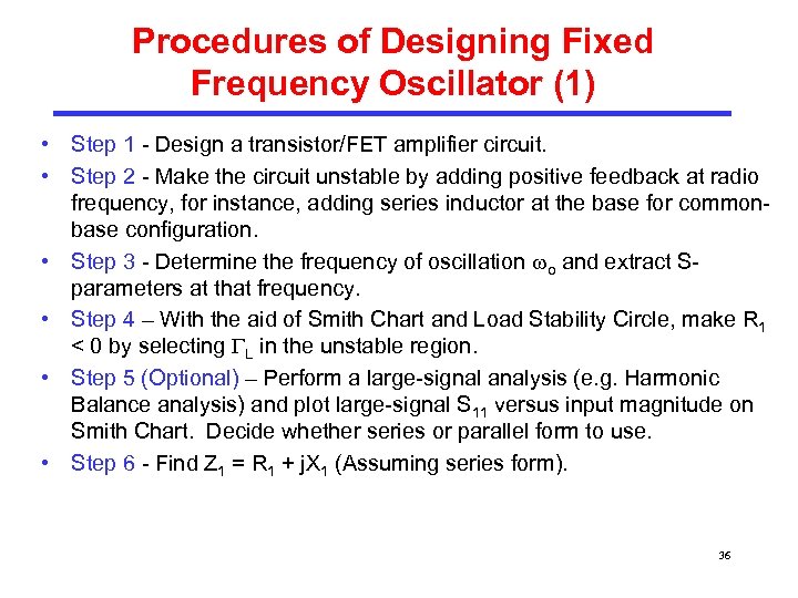 Procedures of Designing Fixed Frequency Oscillator (1) • Step 1 - Design a transistor/FET amplifier circuit. • Step 2 - Make the circuit unstable by adding positive feedback at radio frequency, for instance, adding series inductor at the base for commonbase configuration. • Step 3 - Determine the frequency of oscillation o and extract Sparameters at that frequency. • Step 4 – With the aid of Smith Chart and Load Stability Circle, make R 1 < 0 by selecting L in the unstable region. • Step 5 (Optional) – Perform a large-signal analysis (e. g. Harmonic Balance analysis) and plot large-signal S 11 versus input magnitude on Smith Chart. Decide whether series or parallel form to use. • Step 6 - Find Z 1 = R 1 + j. X 1 (Assuming series form). 36
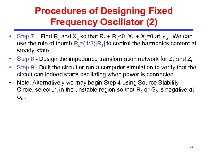 Procedures of Designing Fixed Frequency Oscillator (2) • Step 7 – Find Rs and Xs so that R 1 + Rs<0, X 1 + Xs=0 at o. We can use the rule of thumb Rs=(1/3)|R 1| to control the harmonics content at steady-state. • Step 8 - Design the impedance transformation network for Zs and ZL. • Step 9 - Built the circuit or run a computer simulation to verify that the circuit can indeed starts oscillating when power is connected. • Note: Alternatively we may begin Step 4 using Source Stability Circle, select s in the unstable region so that R 2 or G 2 is negative at o. 37
 Making an Amplifier Unstable (1) • An amplifier can be made unstable by providing some kind of local positive feedback. • Two favorite transistor amplifier configurations used for oscillator design are the Common-Base configuration with Base feedback and Common-Emitter configuration with Emitter degeneration. 38
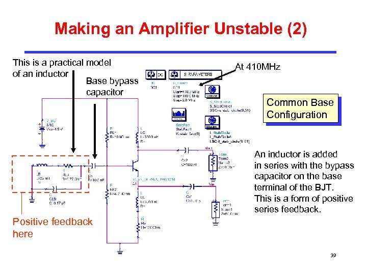 Making an Amplifier Unstable (2) This is a practical model of an inductor Base bypass capacitor At 410 MHz Common Base Configuration An inductor is added in series with the bypass capacitor on the base terminal of the BJT. This is a form of positive series feedback. Positive feedback here 39
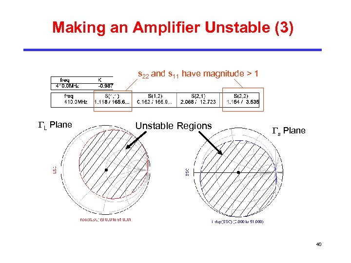 Making an Amplifier Unstable (3) s 22 and s 11 have magnitude > 1 L Plane Unstable Regions s Plane 40
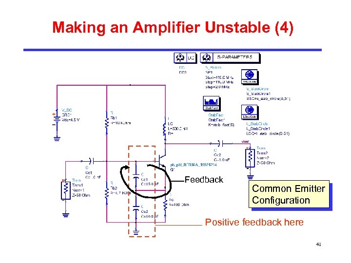 Making an Amplifier Unstable (4) Feedback Common Emitter Configuration Positive feedback here 41
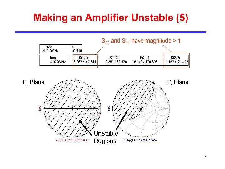 Making an Amplifier Unstable (5) S 22 and S 11 have magnitude > 1 L Plane s Plane Unstable Regions 42
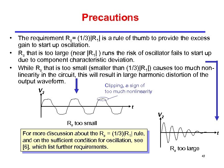 Precautions • The requirement Rs= (1/3)|R 1| is a rule of thumb to provide the excess gain to start up oscillation. • Rs that is too large (near |R 1| ) runs the risk of oscillator fails to start up due to component characteristic deviation. • While Rs that is too small (smaller than (1/3)|R 1|) causes too much nonlinearity in the circuit, this will result in large harmonic distortion of the output waveform. Clipping, a sign of too much nonlinearity V 2 t V 2 Rs too small For more discussion about the Rs = (1/3)|R 1| rule, and on the sufficient condition for oscillation, see [6], which list further requirements. t Rs too large 43
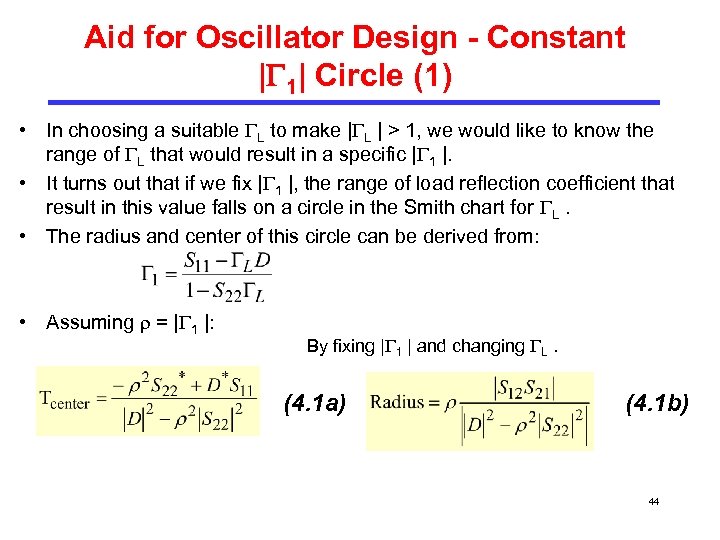 Aid for Oscillator Design - Constant | 1| Circle (1) • In choosing a suitable L to make | L | > 1, we would like to know the range of L that would result in a specific | 1 |. • It turns out that if we fix | 1 |, the range of load reflection coefficient that result in this value falls on a circle in the Smith chart for L. • The radius and center of this circle can be derived from: • Assuming = | 1 |: By fixing | 1 | and changing L. (4. 1 a) (4. 1 b) 44
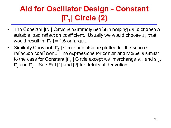 Aid for Oscillator Design - Constant | 1| Circle (2) • The Constant | 1 | Circle is extremely useful in helping us to choose a suitable load reflection coefficient. Usually we would choose L that would result in | 1 | = 1. 5 or larger. • Similarly Constant | 2 | Circle can also be plotted for the source reflection coefficient. The expressions for center and radius is similar to the case for Constant | 1 | Circle except we interchange s 11 and s 22, L and s. See Ref [1] and [2] for details of derivation. 45
 Example 4. 1 – CB Fixed Frequency Oscillator Design • In this example, the design of a fixed frequency oscillator operating at 410 MHz will be demonstrated using BFR 92 A transistor in SOT 23 package. The transistor will be biased in Common-Base configuration. • It is assumed that a 50 load will be connected to the output of the oscillator. The schematic of the basic amplifier circuit is as shown in the following slide. • The design is performed using Agilent’s ADS software, but the author would like to stress that virtually any RF CAD package is suitable for this exercise. 46
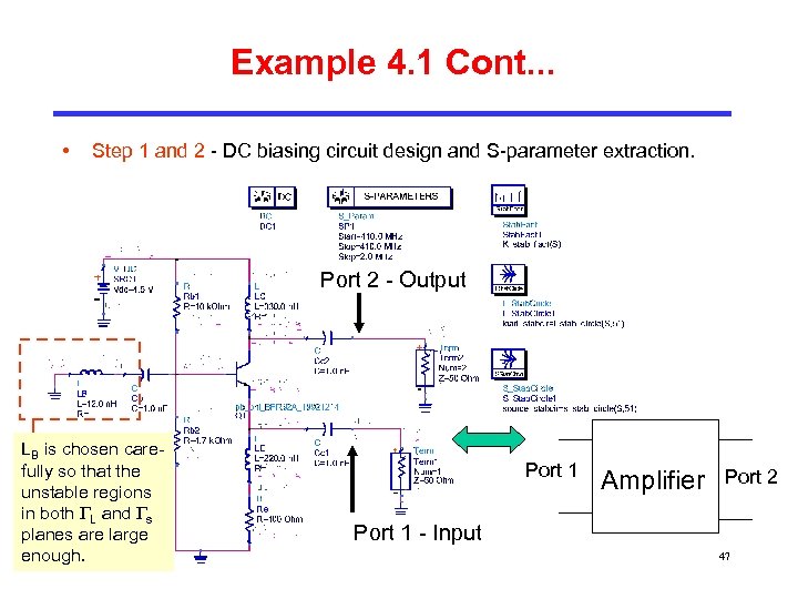 Example 4. 1 Cont. . . • Step 1 and 2 - DC biasing circuit design and S-parameter extraction. Port 2 - Output LB is chosen carefully so that the unstable regions in both L and s planes are large enough. Port 1 Amplifier Port 2 Port 1 - Input 47
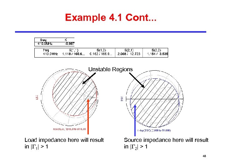 Example 4. 1 Cont. . . Unstable Regions Load impedance here will result in | 1| > 1 Source impedance here will result in | 2| > 1 48
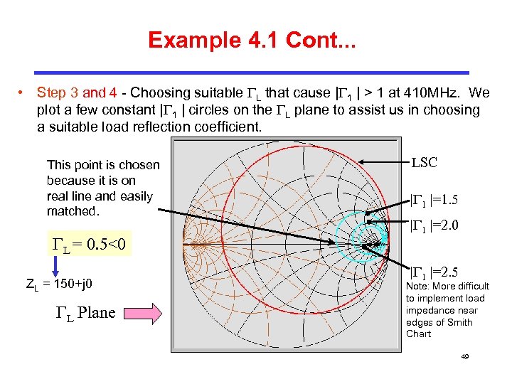 Example 4. 1 Cont. . . • Step 3 and 4 - Choosing suitable L that cause | 1 | > 1 at 410 MHz. We plot a few constant | 1 | circles on the L plane to assist us in choosing a suitable load reflection coefficient. This point is chosen because it is on real line and easily matched. L = 0. 5<0 ZL = 150+j 0 L Plane LSC | 1 |=1. 5 | 1 |=2. 0 | 1 |=2. 5 Note: More difficult to implement load impedance near edges of Smith Chart 49
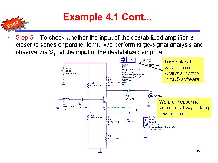 tra Example 4. 1 Cont. . . Ex • Step 5 – To check whether the input of the destabilized amplifier is closer to series or parallel form. We perform large-signal analysis and observe the S 11 at the input of the destabilized amplifier. Large-signal S-parameter Analysis control in ADS software. We are measuring large-signal S 11 looking towards here 50
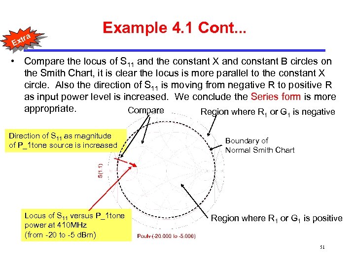 tra Example 4. 1 Cont. . . Ex • Compare the locus of S 11 and the constant X and constant B circles on the Smith Chart, it is clear the locus is more parallel to the constant X circle. Also the direction of S 11 is moving from negative R to positive R as input power level is increased. We conclude the Series form is more appropriate. Compare Region where R or G is negative 1 Direction of S 11 as magnitude of P_1 tone source is increased Locus of S 11 versus P_1 tone power at 410 MHz (from -20 to -5 d. Bm) 1 Boundary of Normal Smith Chart Region where R 1 or G 1 is positive 51
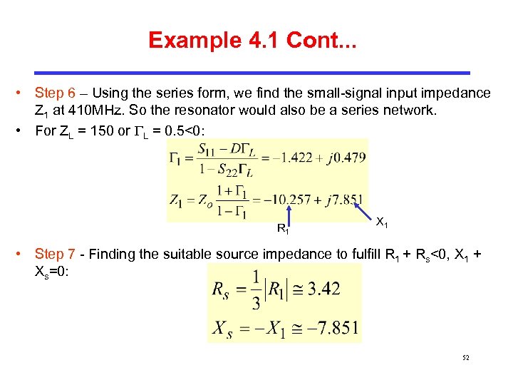 Example 4. 1 Cont. . . • Step 6 – Using the series form, we find the small-signal input impedance Z 1 at 410 MHz. So the resonator would also be a series network. • For ZL = 150 or L = 0. 5<0: R 1 X 1 • Step 7 - Finding the suitable source impedance to fulfill R 1 + Rs<0, X 1 + Xs=0: 52
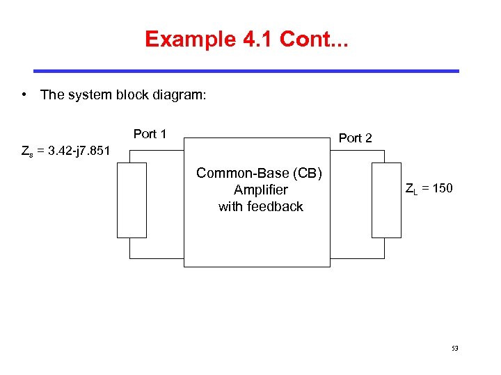 Example 4. 1 Cont. . . • The system block diagram: Port 1 Port 2 Zs = 3. 42 -j 7. 851 Common-Base (CB) Amplifier with feedback ZL = 150 53
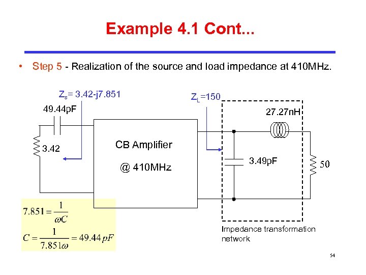 Example 4. 1 Cont. . . • Step 5 - Realization of the source and load impedance at 410 MHz. Zs= 3. 42 -j 7. 851 49. 44 p. F 3. 42 ZL=150 27. 27 n. H CB Amplifier @ 410 MHz 3. 49 p. F 50 Impedance transformation network 54
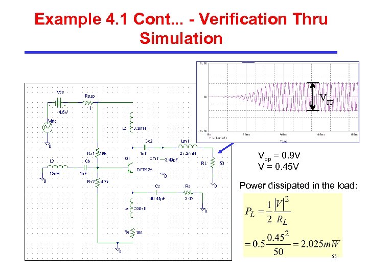 Example 4. 1 Cont. . . - Verification Thru Simulation Vpp BFR 92 A Vpp = 0. 9 V V = 0. 45 V Power dissipated in the load: 55
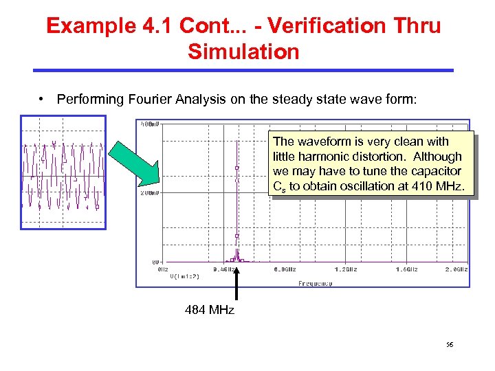 Example 4. 1 Cont. . . - Verification Thru Simulation • Performing Fourier Analysis on the steady state wave form: The waveform is very clean with little harmonic distortion. Although we may have to tune the capacitor Cs to obtain oscillation at 410 MHz. 484 MHz 56
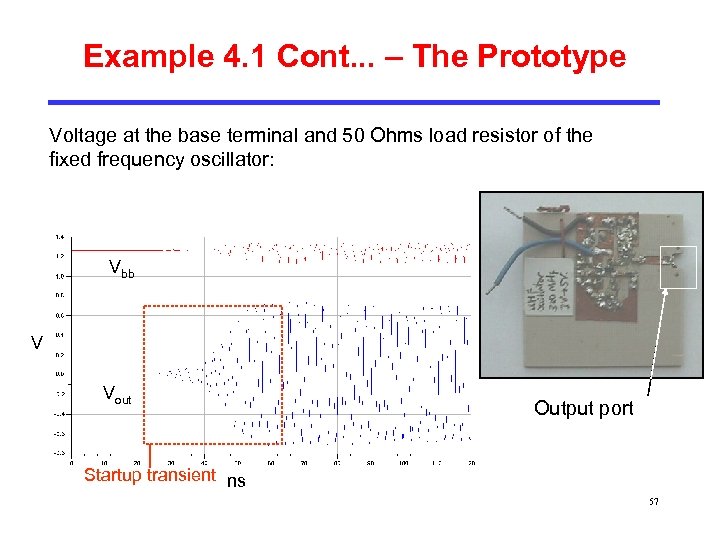 Example 4. 1 Cont. . . – The Prototype Voltage at the base terminal and 50 Ohms load resistor of the fixed frequency oscillator: Vbb V Vout Output port Startup transient ns 57
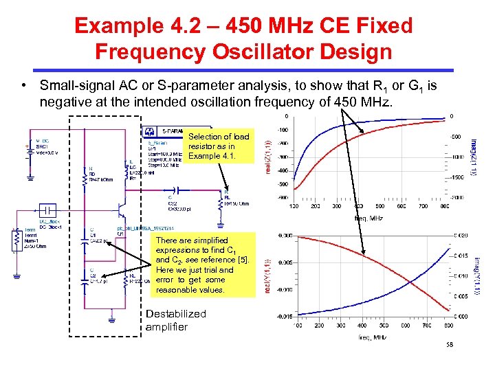 Example 4. 2 – 450 MHz CE Fixed Frequency Oscillator Design • Small-signal AC or S-parameter analysis, to show that R 1 or G 1 is negative at the intended oscillation frequency of 450 MHz. Selection of load resistor as in Example 4. 1. There are simplified expressions to find C 1 and C 2, see reference [5]. Here we just trial and error to get some reasonable values. Destabilized amplifier 58
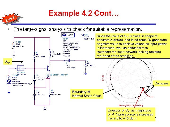 tra Example 4. 2 Cont… Ex • The large-signal analysis to check for suitable representation. Since the locus of S 11 is close in shape to constant X circles, and it indicates R 1 goes from negative value to positive values as input power is increased, we use series form to represent the input network looking towards the Base of the amplifier. S 11 Compare Boundary of Normal Smith Chart Direction of S 11 as magnitude of P_1 tone source is increased 59 from -5 to +15 d. Bm
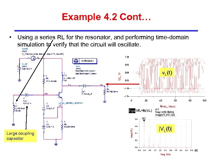 Example 4. 2 Cont… • Using a series RL for the resonator, and performing time-domain simulation to verify that the circuit will oscillate. v. L(t) Large coupling capacitor |VL(f)| 60
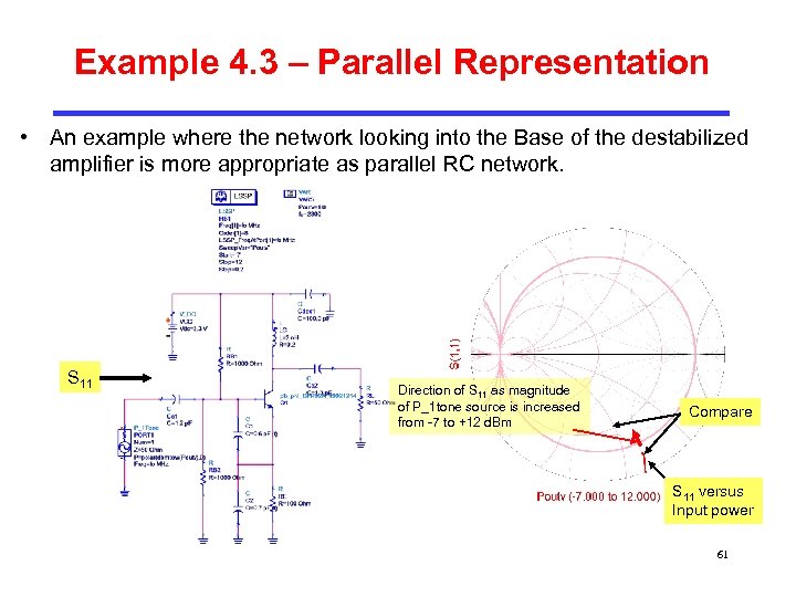 Example 4. 3 – Parallel Representation • An example where the network looking into the Base of the destabilized amplifier is more appropriate as parallel RC network. S 11 Direction of S 11 as magnitude of P_1 tone source is increased from -7 to +12 d. Bm Compare S 11 versus Input power 61
 Frequency Stability • The process of oscillation depends on the non-linear behavior of the negative-resistance network. • The conditions discussed, e. g. equations (3. 1), (3. 8), (3. 9), (3. 10) and (3. 11) are not enough to guarantee a stable state of oscillation. In particular, stability requires that any perturbation in current, voltage and frequency will be damped out, allowing the oscillator to return to it’s initial state. • The stability of oscillation can be expressed in terms of the partial derivative of the sum Zin + Zs or Yin + Ys of the input port (or output port). • The discussion is beyond the scope of this chapter for now, and the reader should refer to [1] and [7] for the concepts. 62
 Some Steps to Improve Oscillator Performance • To improve the frequency stability of the oscillator, the following steps can be taken. • Use components with known temperature coefficients, especially capacitors. • Neutralize, or swamp-out with resistors, the effects of active device variations due to temperature, power supply and circuit load changes. • Operate the oscillator on lower power. • Reduce noise, use shielding, AGC (automatic gain control) and biasline filtering. • Use an oven or temperature compensating circuitry (such as thermistor). • Use differential oscillator architecture (see [4] and [7]). 63
 Extra References for This Section • Some recommended journal papers on frequency stability of oscillator: • Kurokawa K. , “Some basic characteristics of broadband negative resistance oscillator circuits”, Bell System Technical Journal, pp. 19371955, 1969. • Nguyen N. M. , Meyer R. G. , “Start-up and frequency stability in highfrequency oscillators”, IEEE journal of Solid-State Circuits, vol 27, no. 5 pp. 810 -819, 1992. • Grebennikov A. V. , “Stability of negative resistance oscillator circuits”, International journal of Electronic Engineering Education, Vol. 36, pp. 242 -254, 1999. 64
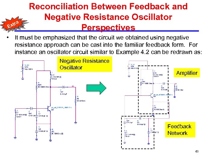 tra Ex Reconciliation Between Feedback and Negative Resistance Oscillator Perspectives • It must be emphasized that the circuit we obtained using negative resistance approach can be cast into the familiar feedback form. For instance an oscillator circuit similar to Example 4. 2 can be redrawn as: Negative Resistance Oscillator Amplifier Feedback Network 65
 5. 0 Voltage Controlled Oscillator 66
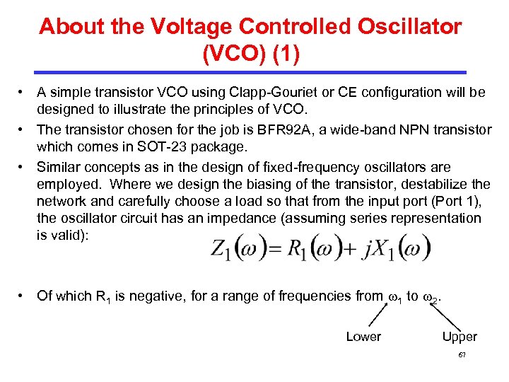 About the Voltage Controlled Oscillator (VCO) (1) • A simple transistor VCO using Clapp-Gouriet or CE configuration will be designed to illustrate the principles of VCO. • The transistor chosen for the job is BFR 92 A, a wide-band NPN transistor which comes in SOT-23 package. • Similar concepts as in the design of fixed-frequency oscillators are employed. Where we design the biasing of the transistor, destabilize the network and carefully choose a load so that from the input port (Port 1), the oscillator circuit has an impedance (assuming series representation is valid): • Of which R 1 is negative, for a range of frequencies from 1 to 2. Lower Upper 67
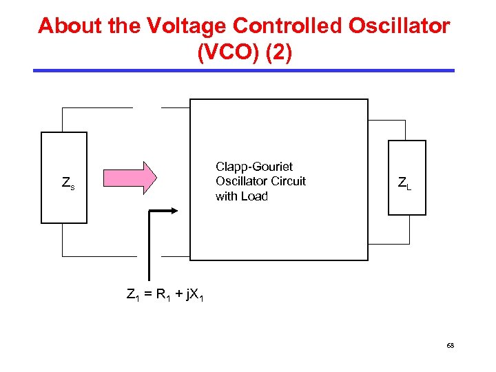 About the Voltage Controlled Oscillator (VCO) (2) Clapp-Gouriet Oscillator Circuit with Load Zs ZL Z 1 = R 1 + j. X 1 68
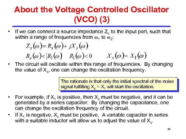 About the Voltage Controlled Oscillator (VCO) (3) • If we can connect a source impedance Zs to the input port, such that within a range of frequencies from 1 to 2: • The circuit will oscillate within this range of frequencies. By changing the value of Xs, one can change the oscillation frequency. The rationale is that only the initial spectral of the noise signal fulfilling Xs = X 1 will start the oscillation. • For example, if X 1 is positive, then Xs must be negative, and it can be generated by a series capacitor. By changing the capacitance, one can change the oscillation frequency of the circuit. • If X 1 is negative, Xs must be positive. A variable capacitor in series with a suitable inductor will allow us to adjust the value of Xs. 69
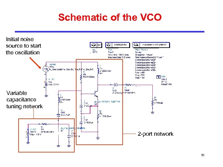 Schematic of the VCO Initial noise source to start the oscillation Variable capacitance tuning network 2 -port network 70
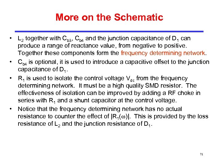 More on the Schematic • L 2 together with Cb 3, Cb 4 and the junction capacitance of D 1 can produce a range of reactance value, from negative to positive. Together these components form the frequency determining network. • Cb 4 is optional, it is used to introduce a capacitive offset to the junction capacitance of D 1. • R 1 is used to isolate the control voltage Vdc from the frequency determining network. It must be a high quality SMD resistor. The effectiveness of isolation can be improved by adding a RF choke in series with R 1 and a shunt capacitor at the control voltage. • Notice that the frequency determining network has no actual resistance to counter the effect of |R 1( )|. This is provided by the loss resistance of L 2 and the junction resistance of D 1. 71
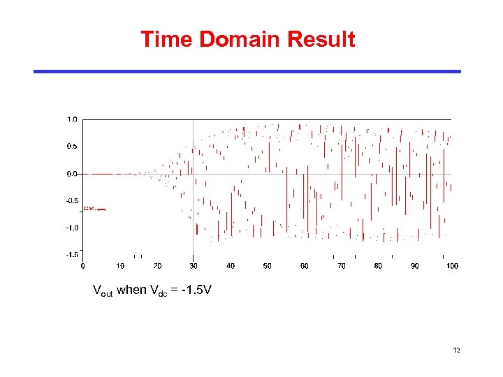 Time Domain Result Vout when Vdc = -1. 5 V 72
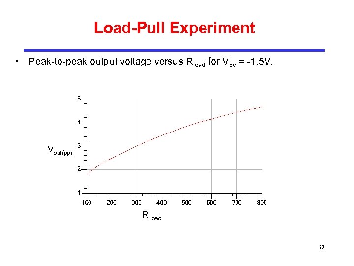 Load-Pull Experiment • Peak-to-peak output voltage versus Rload for Vdc = -1. 5 V. Vout(pp) RLoad 73
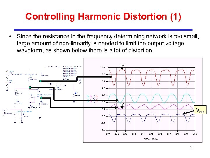 Controlling Harmonic Distortion (1) • Since the resistance in the frequency determining network is too small, large amount of non-linearity is needed to limit the output voltage waveform, as shown below there is a lot of distortion. Vout 74
 Controlling Harmonic Distortion (2) • The distortion generates substantial amount of higher harmonics. • This can be reduced by decreasing the positive feedback, by adding a small capacitance across the collector and base of transistor Q 1. This is shown in the next slide. 75
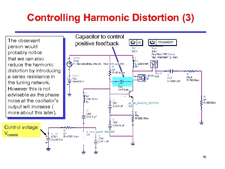 Controlling Harmonic Distortion (3) The observant person would probably notice that we can also reduce the harmonic distortion by introducing a series resistance in the tuning network. However this is not advisable as the phase noise at the oscillator’s output will increase ( more about this later). Capacitor to control positive feedback Control voltage Vcontrol 76
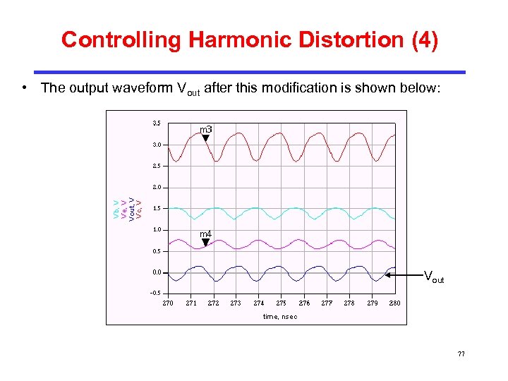 Controlling Harmonic Distortion (4) • The output waveform Vout after this modification is shown below: Vout 77
 Controlling Harmonic Distortion (5) • Finally, it should be noted that we should also add a low-pass filter (LPF) at the output of the oscillator to suppress the higher harmonic components. Such LPF is usually called Harmonic Filter. • Since the oscillator is operating in nonlinear mode, care must be taken in designing the LPF. • Another practical design example will illustrate this approach. 78
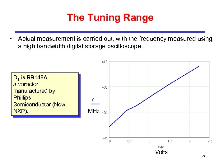 The Tuning Range • Actual measurement is carried out, with the frequency measured using a high bandwidth digital storage oscilloscope. D 1 is BB 149 A, a varactor manufactured by Phillips Semiconductor (Now NXP). MHz Volts 79
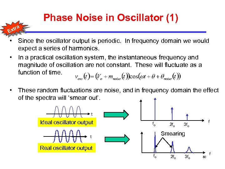 Phase Noise in Oscillator (1) tra Ex • Since the oscillator output is periodic. In frequency domain we would expect a series of harmonics. • In a practical oscillation system, the instantaneous frequency and magnitude of oscillation are not constant. These will fluctuate as a function of time. • These random fluctuations are noise, and in frequency domain the effect of the spectra will ‘smear out’. t Ideal oscillator output fo 2 fo f 3 fo Smearing t Real oscillator output fo 2 fo 3 fo 80 f
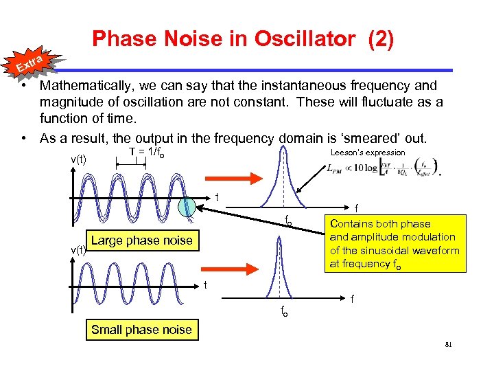 Phase Noise in Oscillator (2) tra Ex • Mathematically, we can say that the instantaneous frequency and magnitude of oscillation are not constant. These will fluctuate as a function of time. • As a result, the output in the frequency domain is ‘smeared’ out. v(t) T = 1/fo Leeson’s expression t fo v(t) Large phase noise f Contains both phase and amplitude modulation of the sinusoidal waveform at frequency fo t fo f Small phase noise 81
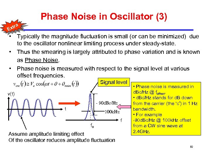 Phase Noise in Oscillator (3) tra Ex • Typically the magnitude fluctuation is small (or can be minimized) due to the oscillator nonlinear limiting process under steady-state. • Thus the smearing is largely attributed to phase variation and is known as Phase Noise. • Phase noise is measured with respect to the signal level at various offset frequencies. Signal level v(t) - 90 d. Bc/Hz t 100 k. Hz fo Assume amplitude limiting effect Of the oscillator reduces amplitude fluctuation f • Phase noise is measured in d. Bc/Hz @ foffset. • d. Bc/Hz stands for d. B down from the carrier (the ‘c’) in 1 Hz bandwidth. • For example -90 d. Bc/Hz @ 100 k. Hz offset from a CW sine wave at 2. 4 GHz. 82
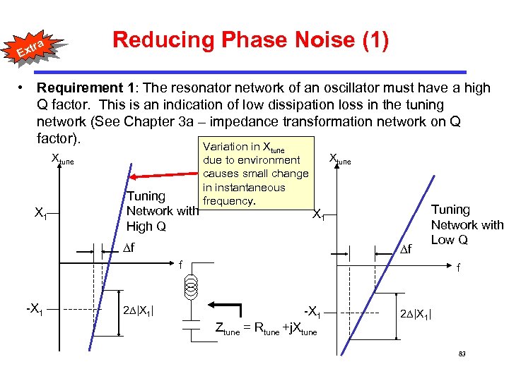 Reducing Phase Noise (1) a tr Ex • Requirement 1: The resonator network of an oscillator must have a high Q factor. This is an indication of low dissipation loss in the tuning network (See Chapter 3 a – impedance transformation network on Q factor). Variation in X tune X 1 Tuning Network with High Q due to environment causes small change in instantaneous frequency. Xtune X 1 f f Tuning Network with Low Q f -X 1 2 |X 1| f -X 1 Ztune = Rtune +j. Xtune 2 |X 1| 83
 a tr Ex Reducing Phase Noise (2) • A Q factor in the tuning network of at least 20 is needed for medium performance oscillator circuits at UHF. For highly stable oscillator, Q factor of the tuning network must be in excess or 1000. • We have looked at LC tuning networks, which can give Q factor of up to 40. Ceramic resonator can provide Q factor greater than 500, while piezoelectric crystal can provide Q factor > 10000. • At microwave frequency, the LC tuning networks can be substituted with transmission line sections. • See R. W. Rhea, “Oscillator design & computer simulation”, 2 nd edition 1995, Mc. Graw-Hill, or the book by R. E. Collin for more discussions on Q factor. • Requirement 2: The power supply to the oscillator circuit should also be very stable to prevent unwanted amplitude modulation at the oscillator’s output. 84
 a tr Ex Reducing Phase Noise (3) • Requirement 3: The voltage level of Vcontrol should be stable. • Requirement 4: The circuit has to be properly shielded from electromagnetic interference from other modules. • Requirement 5: Use low noise components in the construction of the oscillator, e. g. small resistance values, low-loss capacitors and inductors, low-loss PCB dielectric, use discrete components instead of integrated circuits. 85
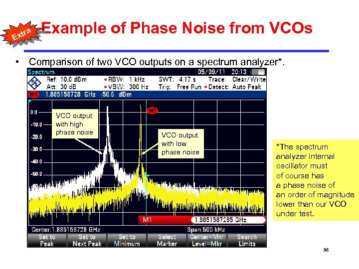 a tr Ex Example of Phase Noise from VCOs • Comparison of two VCO outputs on a spectrum analyzer*. VCO output with high phase noise VCO output with low phase noise *The spectrum analyzer internal oscillator must of course has a phase noise of an order of magnitude lower than our VCO under test. 86
 a tr Ex More Materials • This short discussion cannot do justice to the material on phase noise. • For instance the mathematical model of phase noise in oscillator and the famous Leeson’s equation is not shown here. You can find further discussion in [4], and some material for further readings on this topic: – D. Schere, “The art of phase noise measurement”, Hewlett Packard RF & Microwave Measurement Symposium, 1985. – T. Lee, A. Hajimiri, “The design of low noise oscillators”, Kluwer, 1999. 87
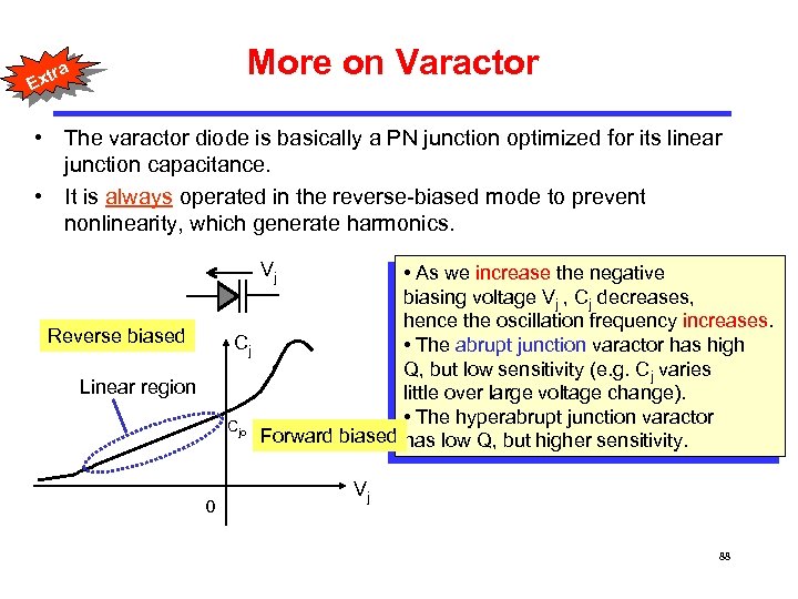 More on Varactor a tr Ex • The varactor diode is basically a PN junction optimized for its linear junction capacitance. • It is always operated in the reverse-biased mode to prevent nonlinearity, which generate harmonics. Vj • As we increase the negative biasing voltage Vj , Cj decreases, hence the oscillation frequency increases. Cj • The abrupt junction varactor has high Q, but low sensitivity (e. g. Cj varies little over large voltage change). • The hyperabrupt junction varactor Cjo Forward biased has low Q, but higher sensitivity. Reverse biased Linear region 0 Vj 88
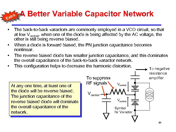 a tr Ex • • A Better Variable Capacitor Network The back-to-back varactors are commonly employed in a VCO circuit, so that at low Vcontrol, when one of the diode is being affected by the AC voltage, the other is still being reverse biased. When a diode is forward biased, the PN junction capacitance becomes nonlinear. The reverse biased diode has smaller junction capacitance, and this dominates the overall capacitance of the back-to-back varactor network. This configuration helps to decrease the harmonic distortion. At any one time, at least one of the diode will be reverse biased. The junction capacitance of the reverse biased diode will dominate the overall capacitance of the network. To suppress RF signals To negative resistance amplifier Vcontrol Symbol for Varactor 89
 Example 5. 1 – VCO Design for Frequency Synthesizer • To design a low power VCO that works from 810 MHz to 910 MHz. • Power supply = 3. 0 V. • Output power (into 50Ω load) minimum -3. 0 d. Bm. 90
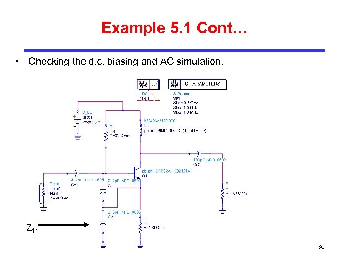 Example 5. 1 Cont… • Checking the d. c. biasing and AC simulation. Z 11 91
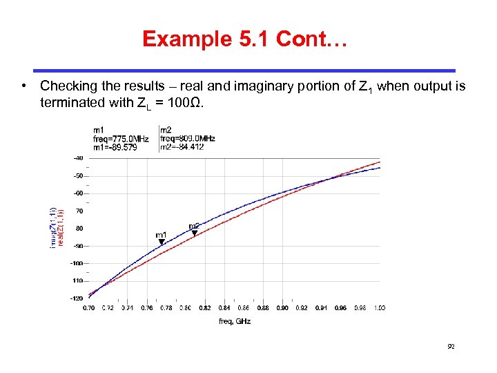 Example 5. 1 Cont… • Checking the results – real and imaginary portion of Z 1 when output is terminated with ZL = 100Ω. 92
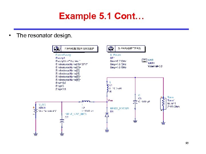 Example 5. 1 Cont… • The resonator design. 93
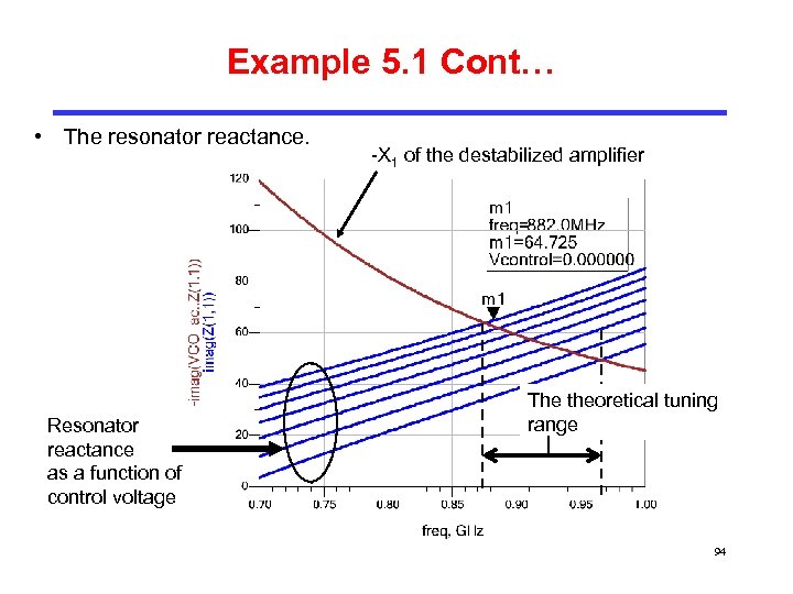 Example 5. 1 Cont… • The resonator reactance. Resonator reactance as a function of control voltage -X 1 of the destabilized amplifier The theoretical tuning range 94
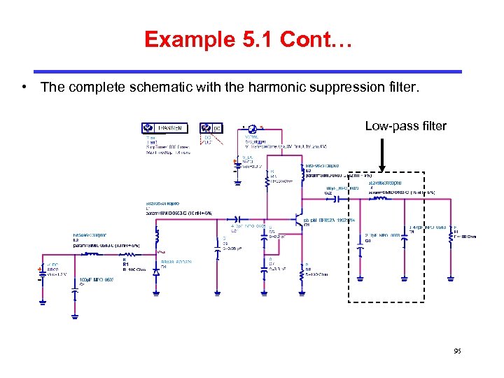 Example 5. 1 Cont… • The complete schematic with the harmonic suppression filter. Low-pass filter 95
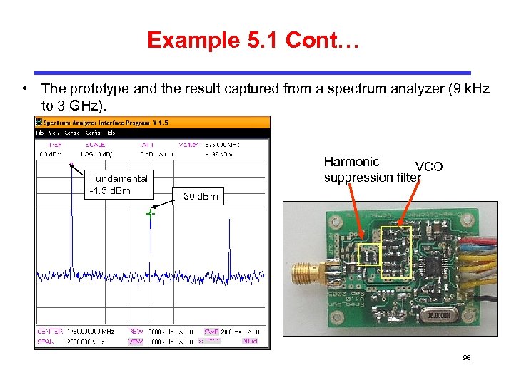 Example 5. 1 Cont… • The prototype and the result captured from a spectrum analyzer (9 k. Hz to 3 GHz). Fundamental -1. 5 d. Bm Harmonic VCO suppression filter - 30 d. Bm 96
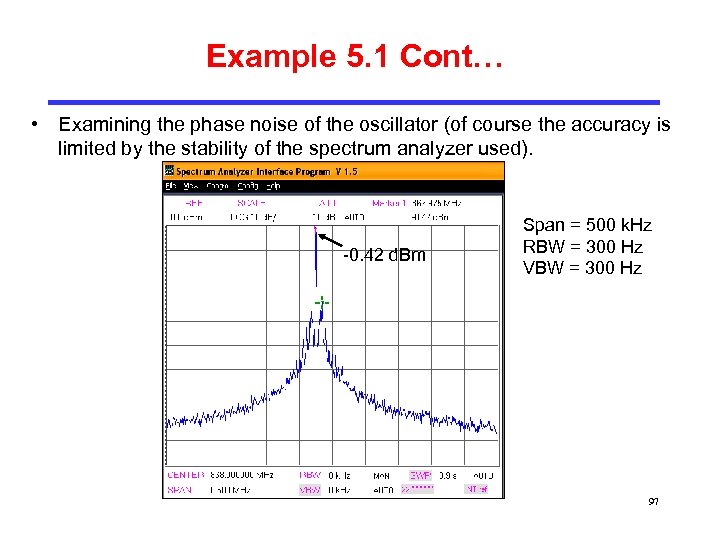 Example 5. 1 Cont… • Examining the phase noise of the oscillator (of course the accuracy is limited by the stability of the spectrum analyzer used). -0. 42 d. Bm Span = 500 k. Hz RBW = 300 Hz VBW = 300 Hz 97
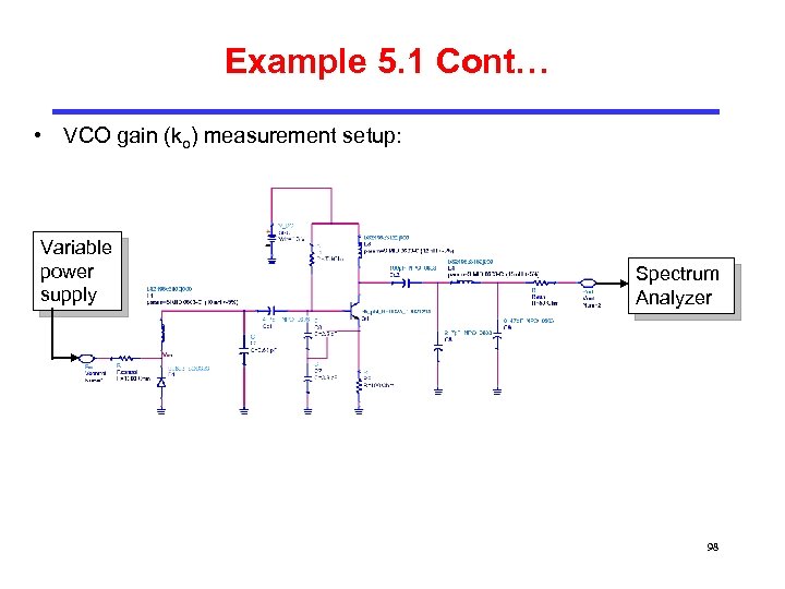 Example 5. 1 Cont… • VCO gain (ko) measurement setup: Variable power supply Spectrum Analyzer 98
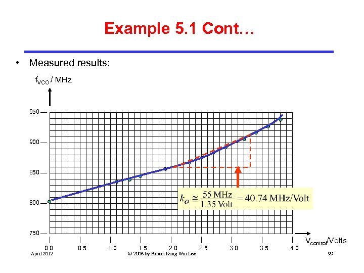 Example 5. 1 Cont… • Measured results: f. VCO / MHz 950 900 850 800 750 0. 0 April 2012 0. 5 1. 0 1. 5 2. 0 2006 by Fabian Kung Wai Lee 2. 5 3. 0 3. 5 4. 0 Vcontrol/Volts 99
![References [1]* D. M. Pozar, “Microwave Engineering”, 2 nd Edition, 1998 John-Wiley & Sons References [1]* D. M. Pozar, “Microwave Engineering”, 2 nd Edition, 1998 John-Wiley & Sons](https://present5.com/presentation/a131d4dd3af3babae992ce7d036cdac9/image-100.jpg) References [1]* D. M. Pozar, “Microwave Engineering”, 2 nd Edition, 1998 John-Wiley & Sons [2] R. Ludwig, P. Bretchko, “RF Circuit Design: Theory and Applications”, 2000 Prentice-Hall [3] B. Razavi, “RF Microelectronics”, 1998 Prentice-Hall, TK 6560 [4] J. R. Smith, “Modern Communication Circuits”, 1998 Mc. Graw-Hill [5] P. H. Young, “Electronics Communication Techniques”, 5 th edition, 2004 Prentice-Hall [6] Gilmore R. , Besser L. , “Practical RF Circuit Design for Modern Wireless Systems”, Vol. 1 & 2, 2003, Artech House
References [1]* D. M. Pozar, “Microwave Engineering”, 2 nd Edition, 1998 John-Wiley & Sons [2] R. Ludwig, P. Bretchko, “RF Circuit Design: Theory and Applications”, 2000 Prentice-Hall [3] B. Razavi, “RF Microelectronics”, 1998 Prentice-Hall, TK 6560 [4] J. R. Smith, “Modern Communication Circuits”, 1998 Mc. Graw-Hill [5] P. H. Young, “Electronics Communication Techniques”, 5 th edition, 2004 Prentice-Hall [6] Gilmore R. , Besser L. , “Practical RF Circuit Design for Modern Wireless Systems”, Vol. 1 & 2, 2003, Artech House


