6fe71bb93ffa89464a6adf958053e08f.ppt
- Количество слайдов: 91
 ME 1000 RF CIRCUIT DESIGN This courseware product contains scholarly and technical information and is protected by copyright laws and international treaties. No part of this publication may be reproduced by any means, be it transmitted, transcribed, photocopied, stored in a retrieval system, or translated into any language in any form, without the prior written permission of Acehub Vista Sdn. Bhd. or their respective copyright owners. The use of the courseware product and all other products developed and/or distributed by Acehub Vista Sdn. Bhd. are subject to the applicable License Agreement. For further information, see the Courseware Product License Agreement. http: //dreamcatcher. asia/cw 1 1
 3 B. RF Microwave Filters 2
 1. 0 Basic Filter Theory 3
 Introduction • An ideal filter is a linear 2 -port network that provides perfect transmission of signal for frequencies in a certain passband region, infinite attenuation for frequencies in the stopband region, and a linear phase response in the passband (to reduce signal distortion). • The goal of filter design is to approximate the ideal requirements within acceptable tolerance with circuits or systems consisting of real components. 4
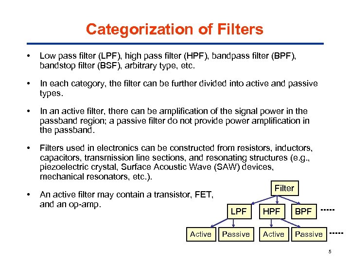 Categorization of Filters • Low pass filter (LPF), high pass filter (HPF), bandpass filter (BPF), bandstop filter (BSF), arbitrary type, etc. • In each category, the filter can be further divided into active and passive types. • In an active filter, there can be amplification of the signal power in the passband region; a passive filter do not provide power amplification in the passband. • Filters used in electronics can be constructed from resistors, inductors, capacitors, transmission line sections, and resonating structures (e. g. , piezoelectric crystal, Surface Acoustic Wave (SAW) devices, mechanical resonators, etc. ). Filter An active filter may contain a transistor, FET, and an op-amp. LPF HPF BPF • Active Passive 5
 Filter Frequency Response • Frequency response implies the behavior of the filter with respect to steady-state sinusoidal excitation (e. g. , energizing the filter with a sine voltage or current source and observing its output). • There are various approaches to displaying the frequency response: – – Transfer function H( ) (the traditional approach) Attenuation factor A( ) S-parameters, e. g. , s 21( ) Others, such as ABCD parameters, etc. 6
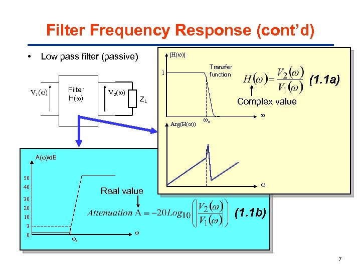 Filter Frequency Response (cont’d) • |H( )| Low pass filter (passive) Transfer function 1 V 1( ) Filter H( ) V 2( ) ZL (1. 1 a) Complex value Arg(H( )) c A( )/d. B 50 40 Real value 30 20 10 3 0 c (1. 1 b) c 7
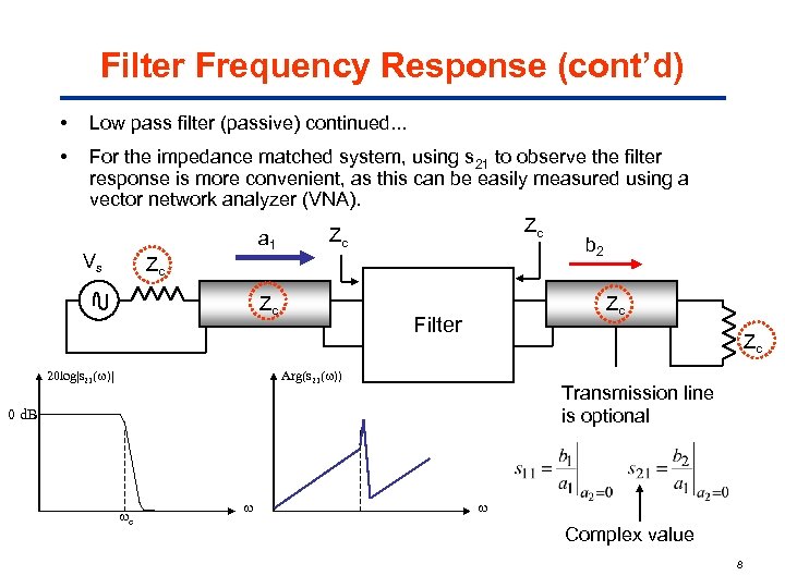 Filter Frequency Response (cont’d) • • Low pass filter (passive) continued. . . For the impedance matched system, using s 21 to observe the filter response is more convenient, as this can be easily measured using a vector network analyzer (VNA). Zc Zc a 1 b 2 Vs Zc Zc Zc Filter Zc Arg(s 21( )) 20 log|s 21( )| Transmission line is optional 0 d. B c Complex value 8
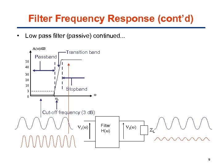 Filter Frequency Response (cont’d) • Low pass filter (passive) continued. . . A( )/d. B 50 40 30 20 10 3 0 Passband Transition band Stopband c Cut-off frequency (3 d. B) V 1( ) Filter H( ) V 2( ) ZL 9
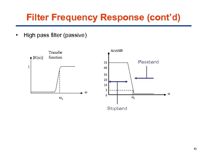 Filter Frequency Response (cont’d) • High pass filter (passive) |H( )| A( )/d. B Transfer function Passband 50 40 1 c 30 20 10 3 0 c Stopband 10
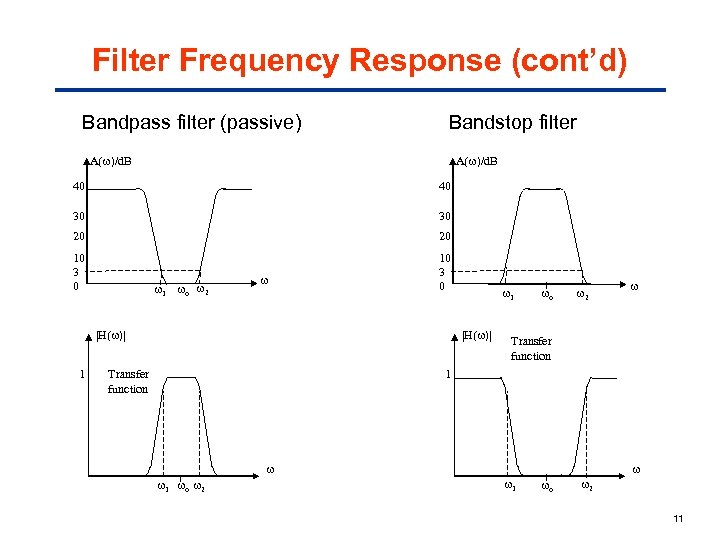 Filter Frequency Response (cont’d) Bandpass filter (passive) Bandstop filter A( )/d. B 40 40 30 30 20 20 10 3 0 1 o 2 |H( )| 1 1 |H( )| Transfer function o 2 Transfer function 1 1 o 2 1 o 2 11
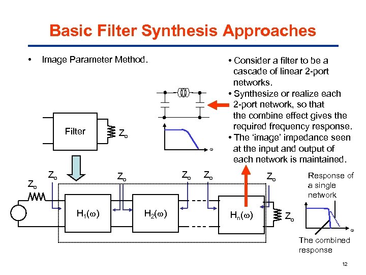 Basic Filter Synthesis Approaches • Image Parameter Method. Filter Zo Zo H 1( ) H 2( ) • Consider a filter to be a cascade of linear 2 -port networks. • Synthesize or realize each 2 -port network, so that the combine effect gives the required frequency response. • The ‘image’ impedance seen at the input and output of each network is maintained. Zo Response of a single network Zo Hn( ) Zo The combined response 12
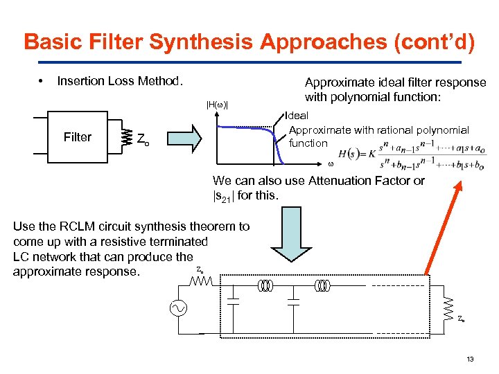 Basic Filter Synthesis Approaches (cont’d) • Insertion Loss Method. |H( )| Filter Zo Approximate ideal filter response with polynomial function: Ideal Approximate with rational polynomial function We can also use Attenuation Factor or |s 21| for this. Use the RCLM circuit synthesis theorem to come up with a resistive terminated LC network that can produce the Z approximate response. o Zo 13
 Our Scope • Only concentrate on passive LC and stripline filters. • Filter synthesis using the Insertion Loss Method (ILM). The Image Parameter Method (IPM) is more efficient and suitable for simple filter designs, but has the disadvantage that arbitrary frequency response cannot be incorporated into the design. 14
 2. 0 Passive LC Filter Synthesis Using the Insertion Loss Method 15
 Insertion Loss Method (ILM) • The insertion loss method (ILM) enables a systematic way to design and synthesize a filter with various frequency responses. • The ILM method also enables a filter performance to be improved in a straightforward manner, at the expense of a ‘higher order’ filter. • A rational polynomial function is used to approximate the ideal |H( )|, A( ), or |s 21( )|. • Phase information is totally ignored. • Ignoring phase simplifies the actual synthesis method. An LC network is then derived which will produce this approximated response. • The attenuation A( ) can be cast into power attenuation ratio, called the Power Loss Ratio, PLR, which is related to A( )2. 16
 a tr Ex More on ILM • There is a historical reason why phase information is ignored. Original filter synthesis methods are developed in the 1920 s– 60 s, for voice communication. The human ear is insensitive to phase distortion, thus only the magnitude response (e. g. , |H( )|, A( )) is considered. • Modern filter synthesis can optimize a circuit to meet both magnitude and phase requirements. This is usually done using computer optimization procedures with ‘goal functions’. 17
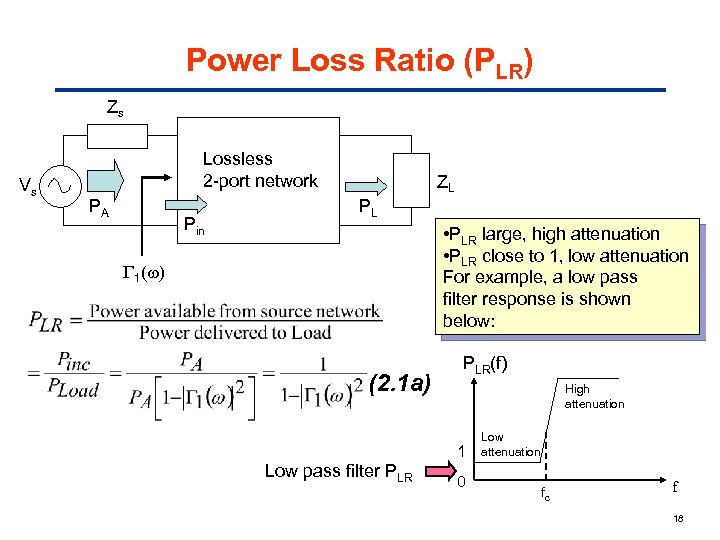 Power Loss Ratio (PLR) Zs Vs Lossless 2 -port network PA Pin ZL PL • PLR large, high attenuation • PLR close to 1, low attenuation For example, a low pass filter response is shown below: 1 (2. 1 a) PLR(f) High attenuation 1 Low pass filter PLR 0 Low attenuation fc f 18
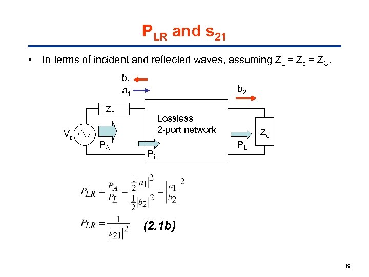 PLR and s 21 • In terms of incident and reflected waves, assuming ZL = Zs = ZC. b 1 a 1 Zc Vs PA b 2 Lossless 2 -port network Pin Zc PL (2. 1 b) 19
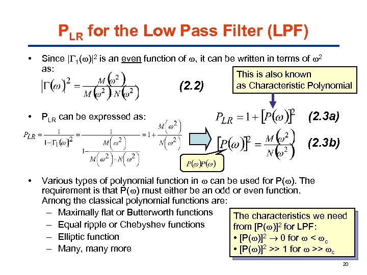 PLR for the Low Pass Filter (LPF) • Since | 1( )|2 is an even function of , it can be written in terms of 2 as: This is also known as Characteristic Polynomial (2. 2) • PLR can be expressed as: (2. 3 a) (2. 3 b) • Various types of polynomial function in can be used for P( ). The requirement is that P( ) must either be an odd or even function. Among the classical polynomial functions are: – Maximally flat or Butterworth functions The characteristics we need – Equal ripple or Chebyshev functions from [P( )]2 for LPF: – Elliptic function • [P( )]2 0 for < c – Many, many more • [P( )]2 >> 1 for >> c 20
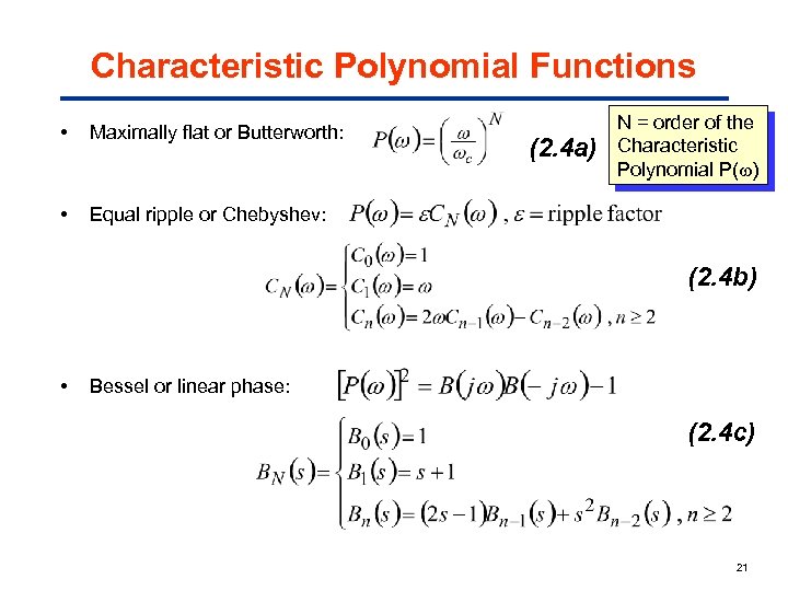 Characteristic Polynomial Functions • Maximally flat or Butterworth: • N = order of the Characteristic Polynomial P( ) Equal ripple or Chebyshev: (2. 4 a) (2. 4 b) • Bessel or linear phase: (2. 4 c) 21
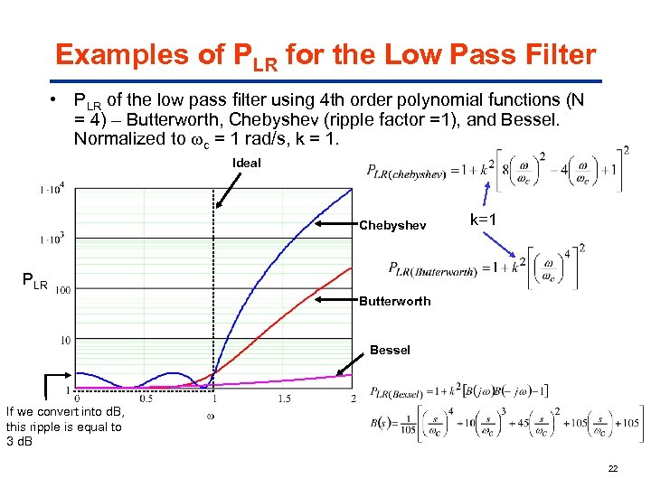 Examples of PLR for the Low Pass Filter • PLR of the low pass filter using 4 th order polynomial functions (N = 4) – Butterworth, Chebyshev (ripple factor =1), and Bessel. Normalized to c = 1 rad/s, k = 1. Ideal Chebyshev k=1 PLR Butterworth Bessel If we convert into d. B, this ripple is equal to 3 d. B 22
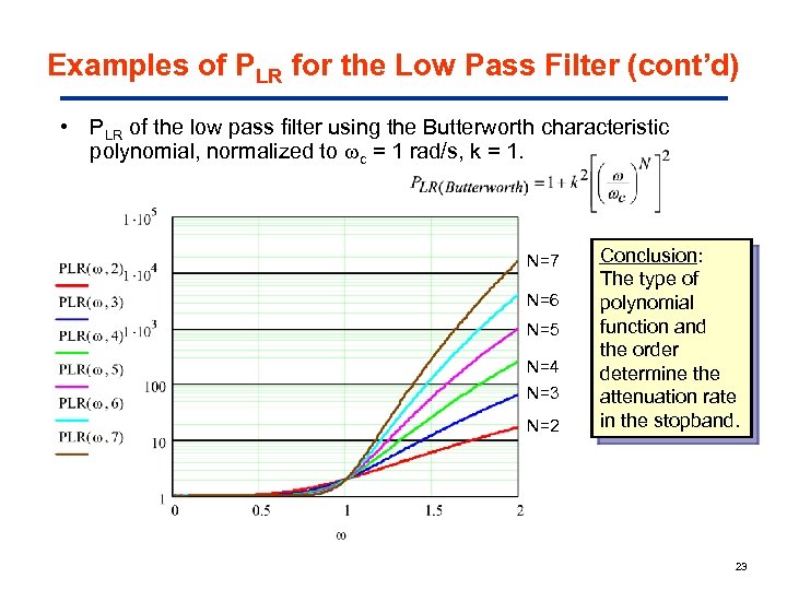 Examples of PLR for the Low Pass Filter (cont’d) • PLR of the low pass filter using the Butterworth characteristic polynomial, normalized to c = 1 rad/s, k = 1. N=7 N=6 N=5 N=4 N=3 N=2 Conclusion: The type of polynomial function and the order determine the attenuation rate in the stopband. 23
 Characteristics of Low Pass Filters Using Various Polynomial Functions • Butterworth: Moderately linear phase response, slow cutoff, smooth attenuation in the passband. • Chebyshev: Bad phase response, rapid cutoff for a similar order, contains ripple in the passband. May have impedance mismatch for N even. • Bessel: Good phase response, linear. Very slow cutoff. Smooth amplitude response in the passband. 24
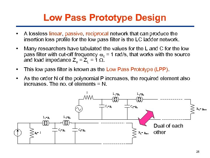 Low Pass Prototype Design • A lossless linear, passive, reciprocal network that can produce the insertion loss profile for the low pass filter is the LC ladder network. • Many researchers have tabulated the values for the L and C for the low pass filter with cut-off frequency c = 1 rad/s, that works with the source and load impedance Zs = ZL = 1 . • This low pass filter is known as the Low Pass Prototype (LPP). • As the order N of the polynomial P increases, the required element also increases. The no. of elements = N. 1 L 1=g 2 C 1=g 1 L 1=g 1 g 0= 1 L 2=g 4 C 2=g 3 RL= g. N+1 L 2=g 3 C 1=g 2 C 2=g 4 RL= g. N+1 Dual of each other 25
 Low Pass Prototype Design (cont’d) • The LPP is the ‘building block’ from which real filters may be constructed. • Various transformations may be used to convert it into a high pass, bandpass, or other filter of arbitrary center frequency and bandwidth. • The following slides show some sample tables for designing LPP for Butterworth and Chebyshev amplitude response of PLR. 26
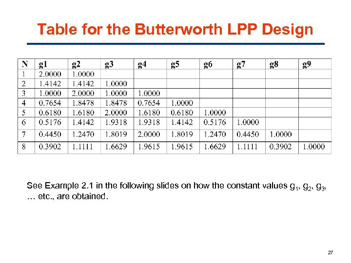 Table for the Butterworth LPP Design See Example 2. 1 in the following slides on how the constant values g 1, g 2, g 3, … etc. , are obtained. 27
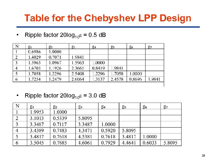 Table for the Chebyshev LPP Design • Ripple factor 20 log 10 = 0. 5 d. B • Ripple factor 20 log 10 = 3. 0 d. B 28
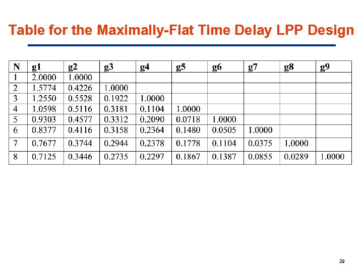 Table for the Maximally-Flat Time Delay LPP Design 29
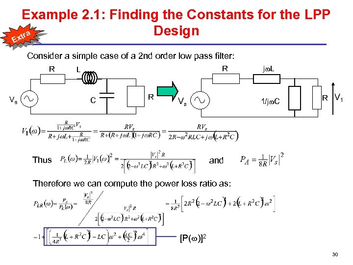 Example 2. 1: Finding the Constants for the LPP Design a xtr E Consider a simple case of a 2 nd order low pass filter: R Vs R L C R Vs Thus j L 1/j C R V 1 and Therefore we can compute the power loss ratio as: [P( )]2 30
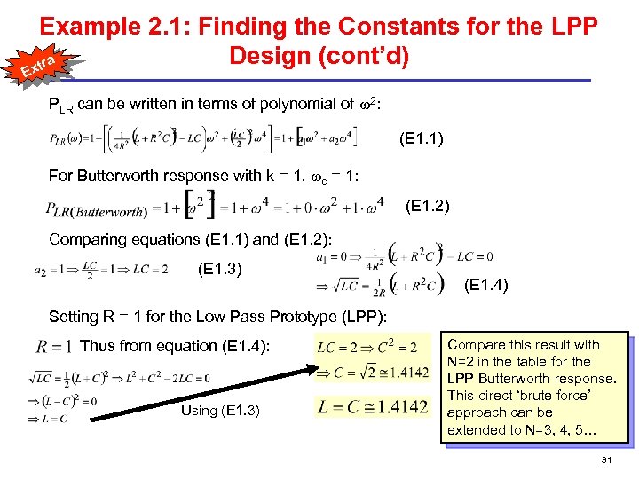 Example 2. 1: Finding the Constants for the LPP Design (cont’d) a xtr E PLR can be written in terms of polynomial of 2: (E 1. 1) For Butterworth response with k = 1, c = 1: (E 1. 2) Comparing equations (E 1. 1) and (E 1. 2): (E 1. 3) (E 1. 4) Setting R = 1 for the Low Pass Prototype (LPP): Thus from equation (E 1. 4): Using (E 1. 3) Compare this result with N=2 in the table for the LPP Butterworth response. This direct ‘brute force’ approach can be extended to N=3, 4, 5… 31
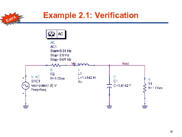 a tr Ex Example 2. 1: Verification 32
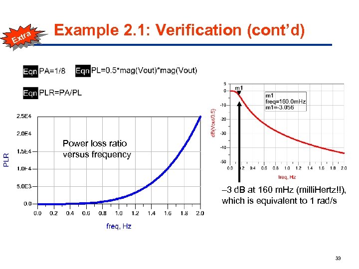 a tr Ex Example 2. 1: Verification (cont’d) Power loss ratio versus frequency – 3 d. B at 160 m. Hz (milli. Hertz!!), which is equivalent to 1 rad/s 33
 Impedance Denormalization and Frequency Transformation of LPP • Once the LPP filter is designed, the cut-off frequency c can be transformed to other frequencies. • Furthermore the LPP can be mapped to other filter types such as high pass, bandpass, and bandstop. • This frequency scaling and transformation entails changing the value and configuration of the elements of the LPP. • Finally the impedance presented by the filter at the operating frequency can also be scaled, from unity to other values; this is called impedance denormalization. • Let Zo be the new system impedance value. The following slide summarizes the various transformation from the LPP filter. 34
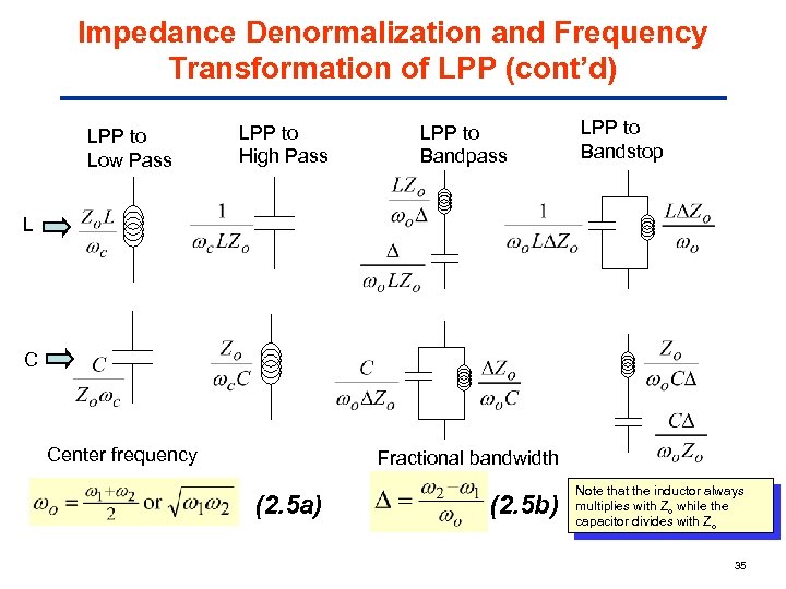 Impedance Denormalization and Frequency Transformation of LPP (cont’d) LPP to Low Pass LPP to High Pass LPP to Bandpass LPP to Bandstop L C Center frequency Fractional bandwidth (2. 5 a) (2. 5 b) Note that the inductor always multiplies with Zo while the capacitor divides with Zo 35
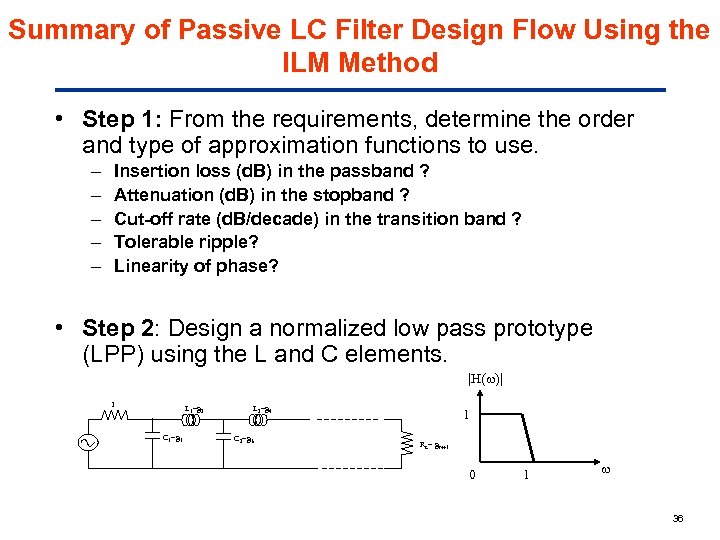 Summary of Passive LC Filter Design Flow Using the ILM Method • Step 1: From the requirements, determine the order and type of approximation functions to use. – – – Insertion loss (d. B) in the passband ? Attenuation (d. B) in the stopband ? Cut-off rate (d. B/decade) in the transition band ? Tolerable ripple? Linearity of phase? • Step 2: Design a normalized low pass prototype (LPP) using the L and C elements. |H( )| 1 L 1=g 2 C 1=g 1 L 2=g 4 C 2=g 3 1 RL= g. N+1 0 1 36
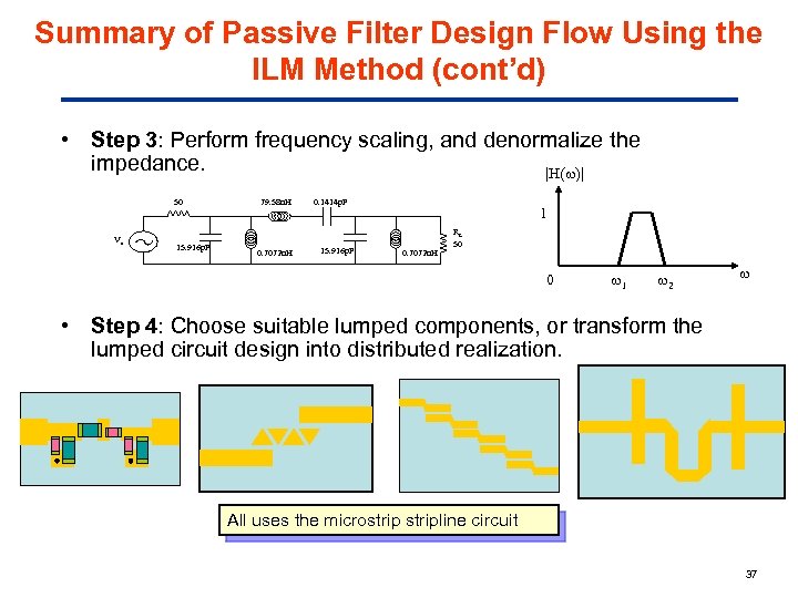 Summary of Passive Filter Design Flow Using the ILM Method (cont’d) • Step 3: Perform frequency scaling, and denormalize the impedance. |H( )| 50 Vs 15. 916 p. F 79. 58 n. H 0. 7072 n. H 0. 1414 p. F 15. 916 p. F 1 0. 7072 n. H RL 50 0 1 2 • Step 4: Choose suitable lumped components, or transform the lumped circuit design into distributed realization. All uses the microstripline circuit 37
 Filter vs. Impedance Transformation Network a tr Ex • If we ponder carefully, the sharp observer will notice that the filter can be considered as a class of impedance transformation network. • In the passband, the load is matched to the source network, much like a filter. • In the stopband, the load impedance is highly mismatched from the source impedance. • However, the procedure described here only applies to the case when both load and source impedance are equal and real. 38
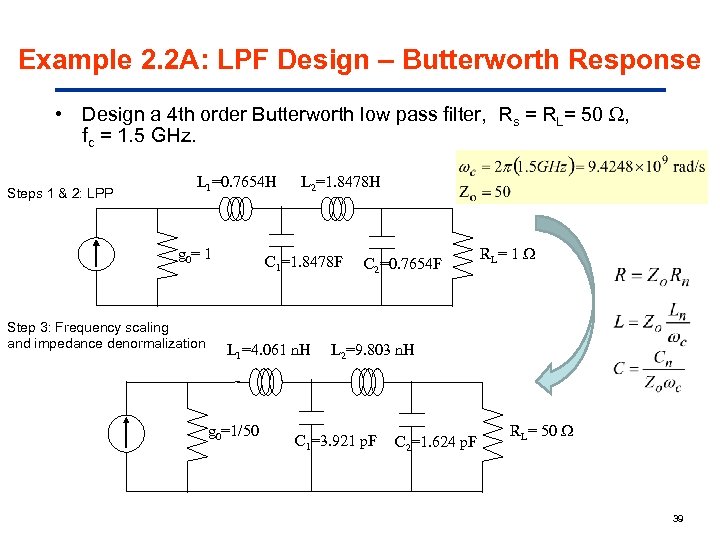 Example 2. 2 A: LPF Design – Butterworth Response • Design a 4 th order Butterworth low pass filter, Rs = RL= 50 , fc = 1. 5 GHz. Steps 1 & 2: LPP L 1=0. 7654 H g 0= 1 Step 3: Frequency scaling and impedance denormalization L 2=1. 8478 H C 1=1. 8478 F L 1=4. 061 n. H g 0=1/50 C 2=0. 7654 F RL = 1 L 2=9. 803 n. H C 1=3. 921 p. F C 2=1. 624 p. F RL= 50 39
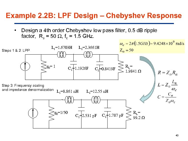 Example 2. 2 B: LPF Design – Chebyshev Response • Design a 4 th order Chebyshev low pass filter, 0. 5 d. B ripple factor, Rs = 50 , fc = 1. 5 GHz. Steps 1 & 2: LPP L 1=1. 6703 H g 0= 1 L 2=2. 3661 H C 1=1. 1926 F Step 3: Frequency scaling and impedance denormalization L =8. 861 n. H 1 g 0=1/50 C 2=0. 8419 F RL = 1. 9841 L 2=12. 55 n. H C 1=2. 531 p. F C 2=1. 787 p. F RL = 99. 2 40
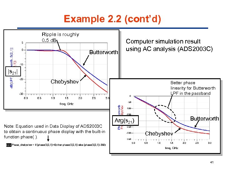 Example 2. 2 (cont’d) Ripple is roughly 0. 5 d. B Butterworth Computer simulation result using AC analysis (ADS 2003 C) |s 21| Chebyshev Note: Equation used in Data Display of ADS 2003 C to obtain a continuous phase display with the built-in function phase( ). Better phase linearity for Butterworth LPF in the passband Butterworth Arg(s 21) Chebyshev 41
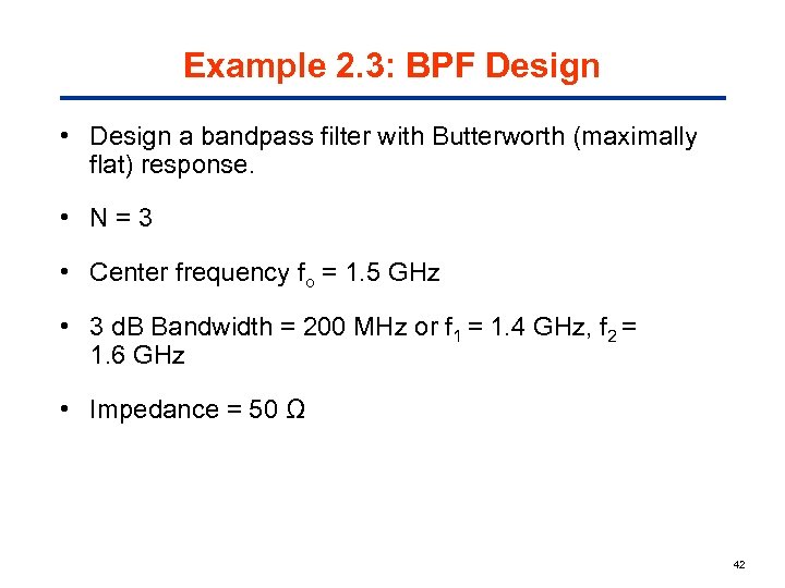 Example 2. 3: BPF Design • Design a bandpass filter with Butterworth (maximally flat) response. • N=3 • Center frequency fo = 1. 5 GHz • 3 d. B Bandwidth = 200 MHz or f 1 = 1. 4 GHz, f 2 = 1. 6 GHz • Impedance = 50 Ω 42
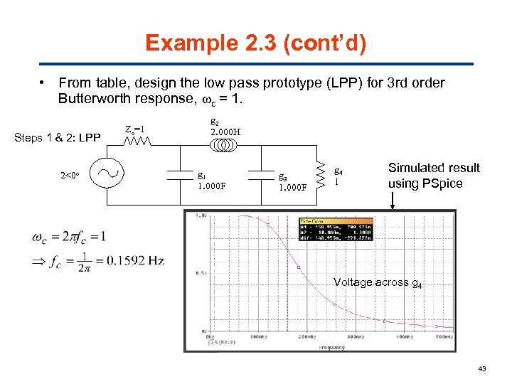 Example 2. 3 (cont’d) • From table, design the low pass prototype (LPP) for 3 rd order Butterworth response, c = 1. Steps 1 & 2: LPP 2<0 o Zo=1 g 2 2. 000 H g 1 1. 000 F g 3 1. 000 F g 4 1 Simulated result using PSpice Voltage across g 4 43
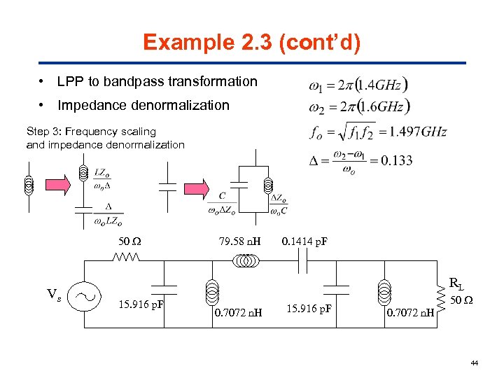 Example 2. 3 (cont’d) • LPP to bandpass transformation • Impedance denormalization Step 3: Frequency scaling and impedance denormalization 50 Vs 79. 58 n. H 0. 1414 p. F RL 15. 916 p. F 0. 7072 n. H 15. 916 p. F 50 0. 7072 n. H 44
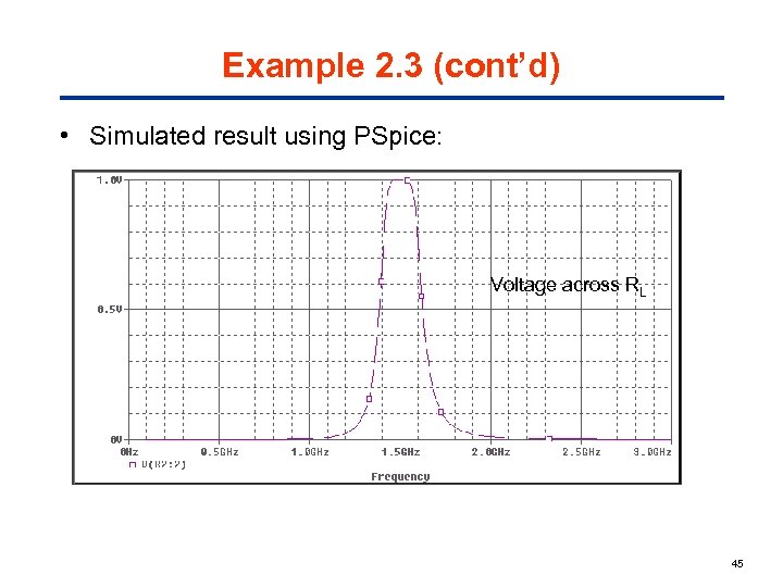 Example 2. 3 (cont’d) • Simulated result using PSpice: Voltage across RL 45
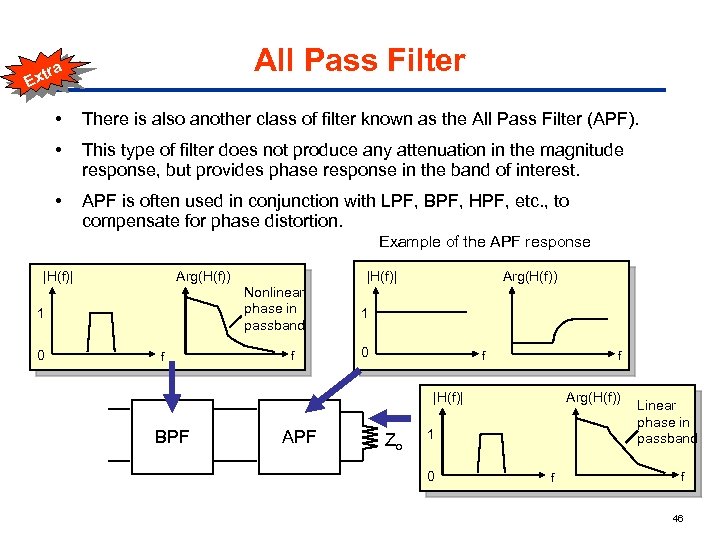 a All Pass Filter • There is also another class of filter known as the All Pass Filter (APF). • This type of filter does not produce any attenuation in the magnitude response, but provides phase response in the band of interest. • APF is often used in conjunction with LPF, BPF, HPF, etc. , to compensate for phase distortion. tr Ex Example of the APF response |H(f)| Arg(H(f)) 1 0 f Nonlinear phase in passband f |H(f)| Arg(H(f)) 1 0 f f Arg(H(f)) |H(f)| BPF APF Zo 1 0 f Linear phase in passband f 46
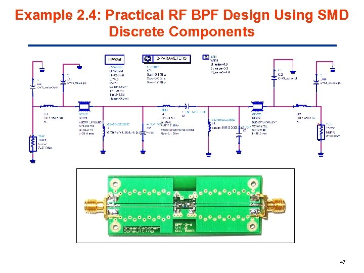 Example 2. 4: Practical RF BPF Design Using SMD Discrete Components 47
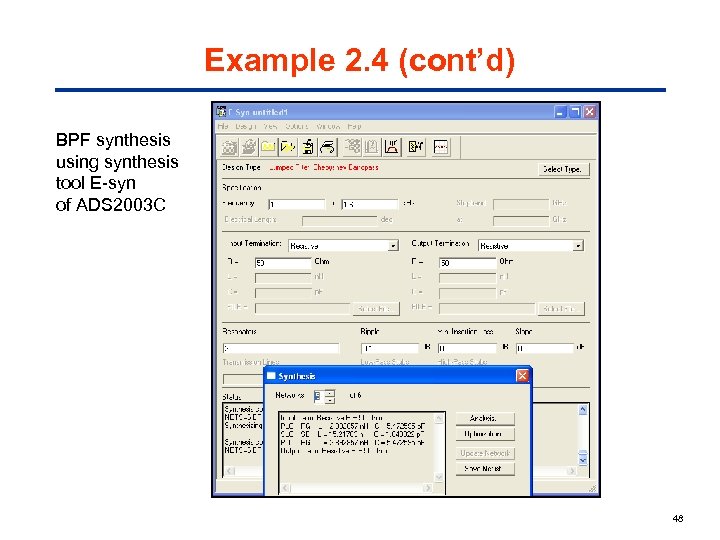 Example 2. 4 (cont’d) BPF synthesis using synthesis tool E-syn of ADS 2003 C 48
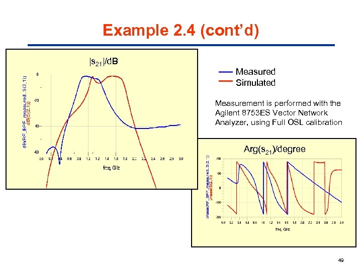 Example 2. 4 (cont’d) |s 21|/d. B Measured Simulated Measurement is performed with the Agilent 8753 ES Vector Network Analyzer, using Full OSL calibration Arg(s 21)/degree 49
 3. 0 Microwave Filter Realization Using Stripline Structures 50
 3. 1 Basic Approach 51
 Filter Realization Using Distributed Circuit Elements • Lumped-element filter realization using surface mounted inductors and capacitors generally works well at lower frequencies (at UHF, say < 3 GHz). • At higher frequencies, the practical inductors and capacitors loses their intrinsic characteristics. • Also, a limited range of component values is available from the manufacturer. • Therefore, for microwave frequencies (> 3 GHz), the passive filter is usually realized using distributed circuit elements such as transmission line sections. • Here we will focus on stripline microwave circuits. 52
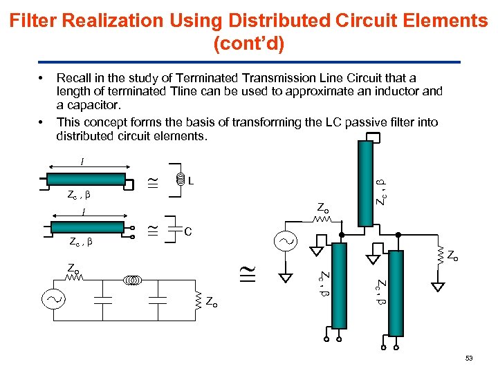 Filter Realization Using Distributed Circuit Elements (cont’d) • Recall in the study of Terminated Transmission Line Circuit that a length of terminated Tline can be used to approximate an inductor and a capacitor. This concept forms the basis of transforming the LC passive filter into distributed circuit elements. l Zc , L Zo Zc , • C Zc , Zo Zc , Zo Zo 53
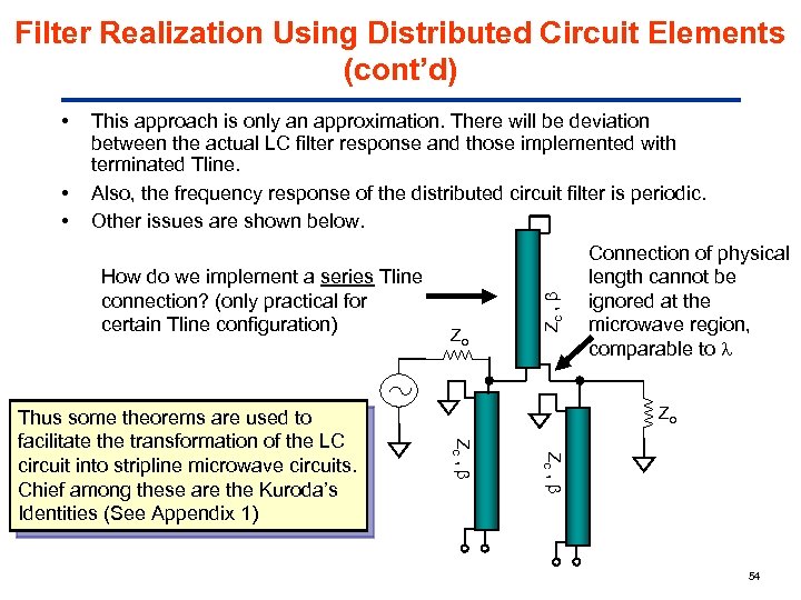 Filter Realization Using Distributed Circuit Elements (cont’d) • • This approach is only an approximation. There will be deviation between the actual LC filter response and those implemented with terminated Tline. Also, the frequency response of the distributed circuit filter is periodic. Other issues are shown below. How do we implement a series Tline connection? (only practical for certain Tline configuration) Connection of physical length cannot be ignored at the microwave region, comparable to Zo Zc , Thus some theorems are used to facilitate the transformation of the LC circuit into stripline microwave circuits. Chief among these are the Kuroda’s Identities (See Appendix 1) Zo Zc , • 54
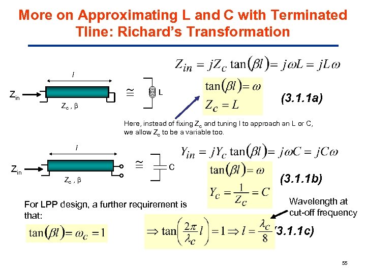 More on Approximating L and C with Terminated Tline: Richard’s Transformation l Zin L (3. 1. 1 a) Zc , Here, instead of fixing Zc and tuning l to approach an L or C, we allow Zc to be a variable too. l Zin C Zc , For LPP design, a further requirement is that: (3. 1. 1 b) Wavelength at cut-off frequency (3. 1. 1 c) 55
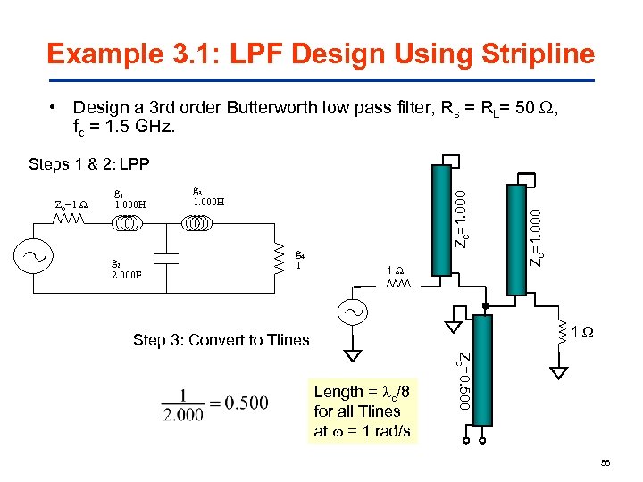 Example 3. 1: LPF Design Using Stripline • Design a 3 rd order Butterworth low pass filter, Rs = RL= 50 , fc = 1. 5 GHz. g 2 2. 000 F g 3 1. 000 H g 4 1 Zc=1. 000 Zo=1 g 1 1. 000 H 1 Zc=1. 000 Steps 1 & 2: LPP 1 Step 3: Convert to Tlines Zc=0. 500 Length = c/8 for all Tlines at = 1 rad/s 56
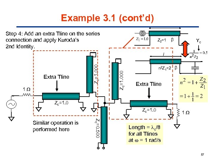 Example 3. 1 (cont’d) Step 4: Add an extra Tline on the series connection and apply Kuroda’s 2 nd Identity. Z 2=1 Yc 1 Zc=1. 000 Extra Tline Zc=1. 000 l n 2 Z 1=2 Extra Tline Zc=1. 0 Zc=0. 500 Similar operation is performed here 1 Length = c/8 for all Tlines at = 1 rad/s 57
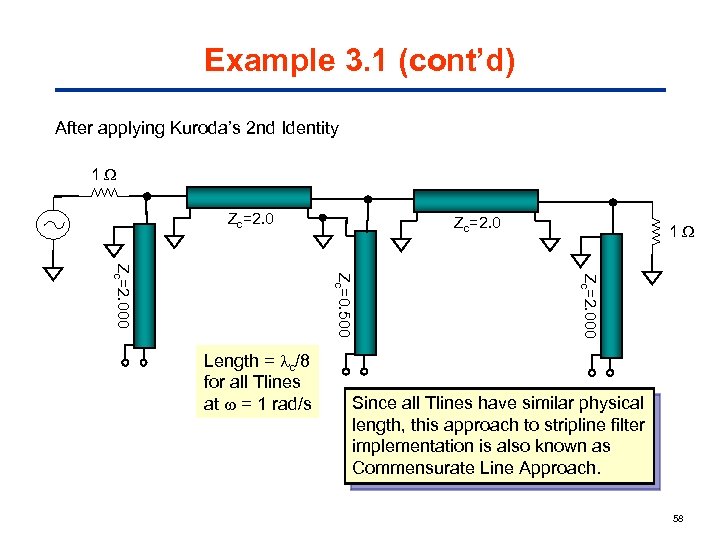 Example 3. 1 (cont’d) After applying Kuroda’s 2 nd Identity 1 Zc=2. 000 Zc=0. 500 Zc=2. 000 Length = c/8 for all Tlines at = 1 rad/s 1 Since all Tlines have similar physical length, this approach to stripline filter implementation is also known as Commensurate Line Approach. 58
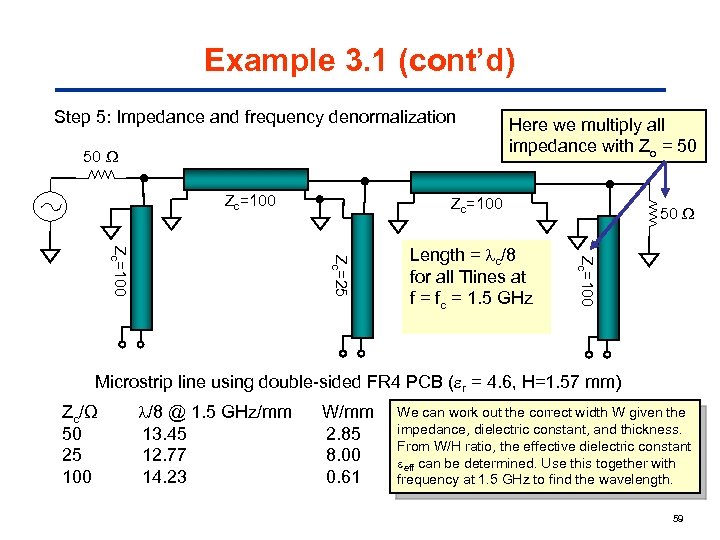 Example 3. 1 (cont’d) Step 5: Impedance and frequency denormalization 50 Zc=100 Here we multiply all impedance with Zo = 50 Zc=100 Zc=25 Zc=100 Length = c/8 for all Tlines at f = fc = 1. 5 GHz 50 Microstrip line using double-sided FR 4 PCB ( r = 4. 6, H=1. 57 mm) Zc/Ω 50 25 100 /8 @ 1. 5 GHz/mm 13. 45 12. 77 14. 23 W/mm 2. 85 8. 00 0. 61 We can work out the correct width W given the impedance, dielectric constant, and thickness. From W/H ratio, the effective dielectric constant eff can be determined. Use this together with frequency at 1. 5 GHz to find the wavelength. 59
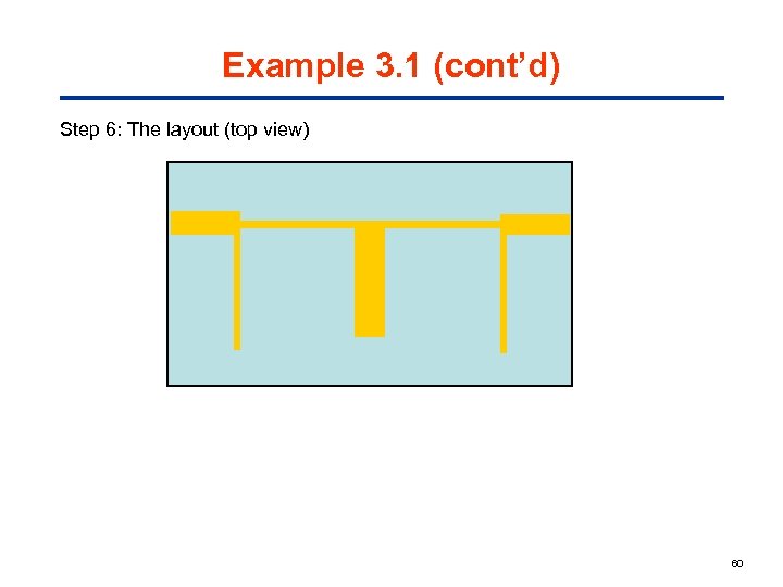 Example 3. 1 (cont’d) Step 6: The layout (top view) 60
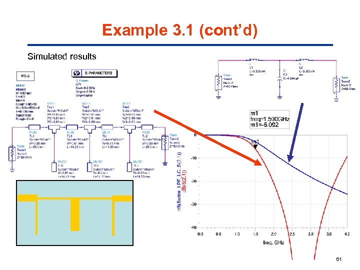 Example 3. 1 (cont’d) Simulated results 61
 Conclusions for Section 3. 1 • Further tuning is needed to optimize the frequency response. • The method illustrated is good for the low pass and bandstop filter implementation. • For high pass and bandpass, other approaches are needed. 62
 3. 2 Further Implementations 63
 Realization of LPF Using the Step-Impedance Approach • A relatively easy way to implement LPF using stripline components. • Using alternating sections of high and low characteristic impedance Tlines to approximate the alternating L and C elements in an LPF. • Performance of this approach is marginal as it is an approximation, where a sharp cutoff is not required. • As usual, beware of parasitic passbands!!! 64
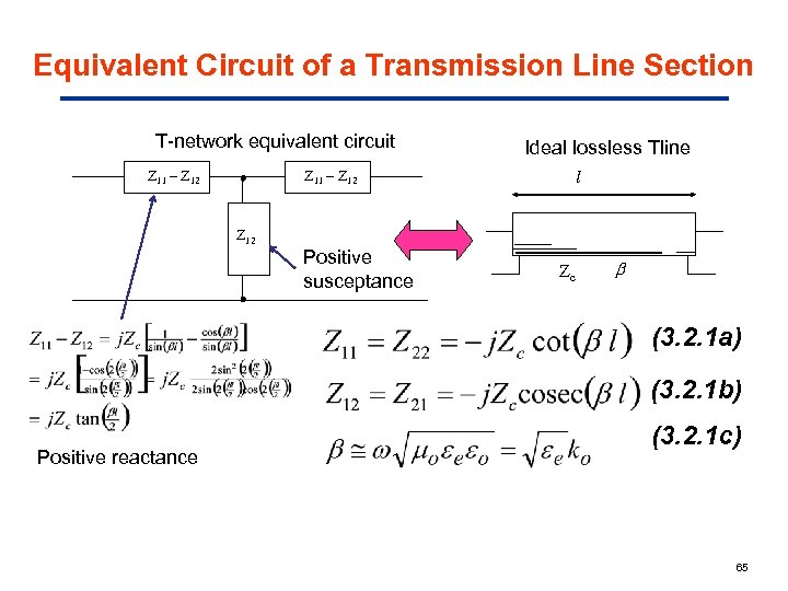 Equivalent Circuit of a Transmission Line Section T-network equivalent circuit Z 11 – Z 12 Ideal lossless Tline Z 11 – Z 12 Positive susceptance l Zc (3. 2. 1 a) (3. 2. 1 b) Positive reactance (3. 2. 1 c) 65
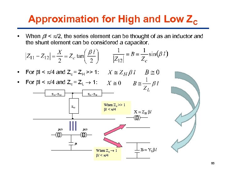 Approximation for High and Low ZC • When l < /2, the series element can be thought of as an inductor and the shunt element can be considered a capacitor. • For l < /4 and Zc = ZH >> 1: • For l < /4 and Zc = ZL 1: Z 11 - Z 12 When Zc >> 1 l < /4 Z 12 j. X/2 X ZH l j. X/2 j. B When Zc 1 l < /4 B YL l 66
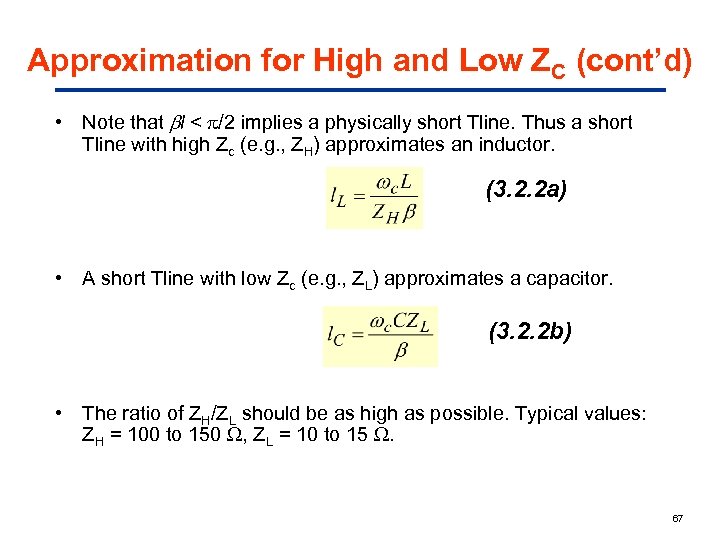 Approximation for High and Low ZC (cont’d) • Note that l < /2 implies a physically short Tline. Thus a short Tline with high Zc (e. g. , ZH) approximates an inductor. (3. 2. 2 a) • A short Tline with low Zc (e. g. , ZL) approximates a capacitor. (3. 2. 2 b) • The ratio of ZH/ZL should be as high as possible. Typical values: ZH = 100 to 150 , ZL = 10 to 15 . 67
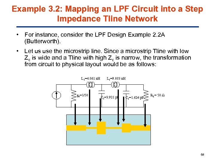 Example 3. 2: Mapping an LPF Circuit into a Step Impedance Tline Network • For instance, consider the LPF Design Example 2. 2 A (Butterworth). • Let us use the microstrip line. Since a microstrip Tline with low Zc is wide and a Tline with high Zc is narrow, the transformation from circuit to physical layout would be as follows: L 1=4. 061 n. H g 0=1/50 L 2=9. 803 n. H C 1=3. 921 p. F C 2=1. 624 p. F RL= 50 68
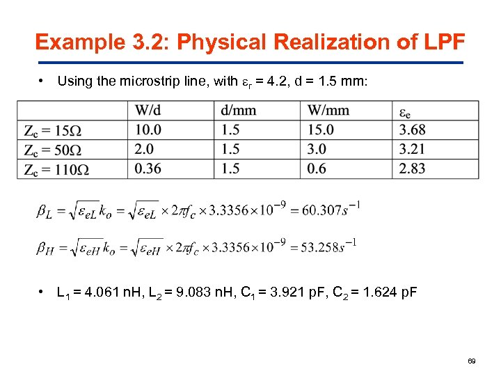 Example 3. 2: Physical Realization of LPF • Using the microstrip line, with r = 4. 2, d = 1. 5 mm: • L 1 = 4. 061 n. H, L 2 = 9. 083 n. H, C 1 = 3. 921 p. F, C 2 = 1. 624 p. F 69
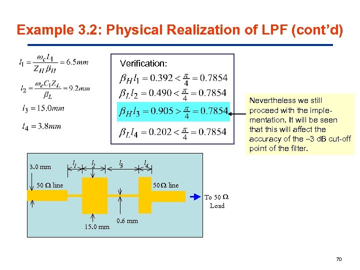 Example 3. 2: Physical Realization of LPF (cont’d) Verification: Nevertheless we still proceed with the implementation. It will be seen that this will affect the accuracy of the – 3 d. B cut-off point of the filter. 3. 0 mm l 1 l 2 l 3 50 line l 4 50 line To 50 Load 15. 0 mm 0. 6 mm 70
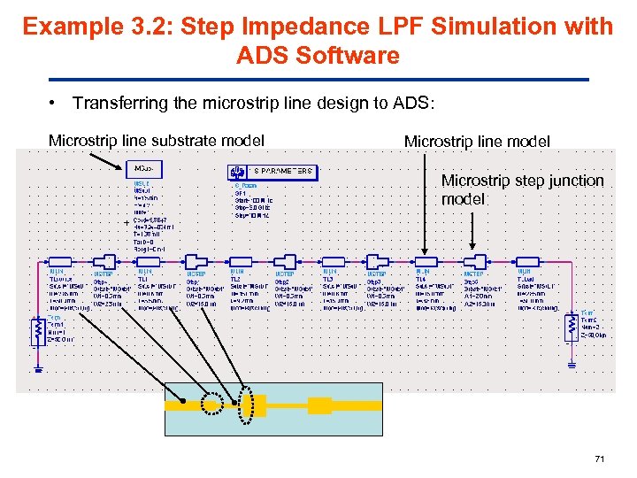 Example 3. 2: Step Impedance LPF Simulation with ADS Software • Transferring the microstrip line design to ADS: Microstrip line substrate model Microstrip line model Microstrip step junction model 71
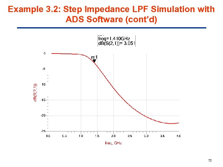 Example 3. 2: Step Impedance LPF Simulation with ADS Software (cont’d) 72
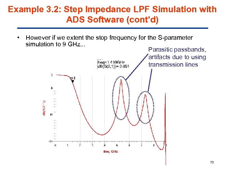 Example 3. 2: Step Impedance LPF Simulation with ADS Software (cont’d) • However if we extent the stop frequency for the S-parameter simulation to 9 GHz. . . Parasitic passbands, artifacts due to using transmission lines 73
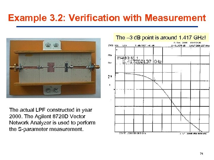 Example 3. 2: Verification with Measurement The – 3 d. B point is around 1. 417 GHz! The actual LPF constructed in year 2000. The Agilent 8720 D Vector Network Analyzer is used to perform the S-parameter measurement. 74
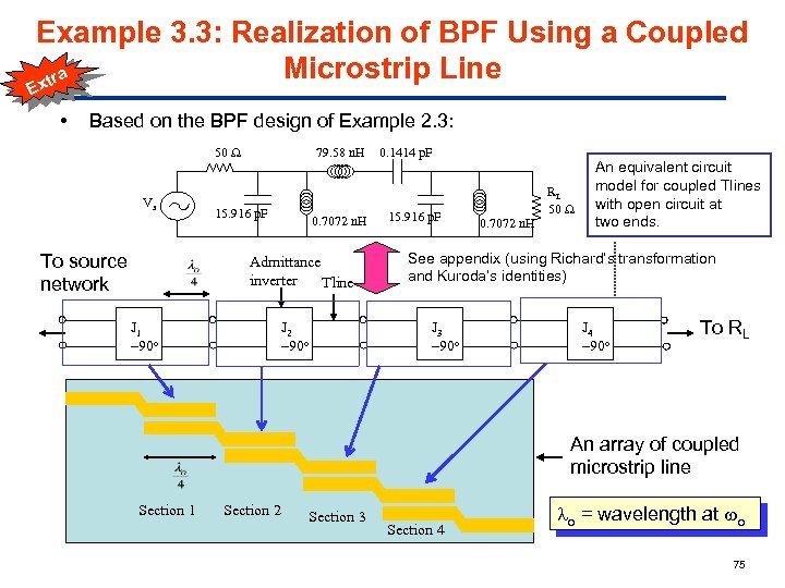 Example 3. 3: Realization of BPF Using a Coupled Microstrip Line a xtr E • Based on the BPF design of Example 2. 3: 50 Vs To source network 79. 58 n. H 15. 916 p. F 0. 7072 n. H Admittance inverter Tline J 1 – 90 o J 2 – 90 o 0. 1414 p. F 15. 916 p. F RL 50 0. 7072 n. H An equivalent circuit model for coupled Tlines with open circuit at two ends. See appendix (using Richard’s transformation and Kuroda’s identities) J 3 – 90 o J 4 – 90 o To RL An array of coupled microstrip line Section 1 Section 2 Section 3 Section 4 o = wavelength at o 75
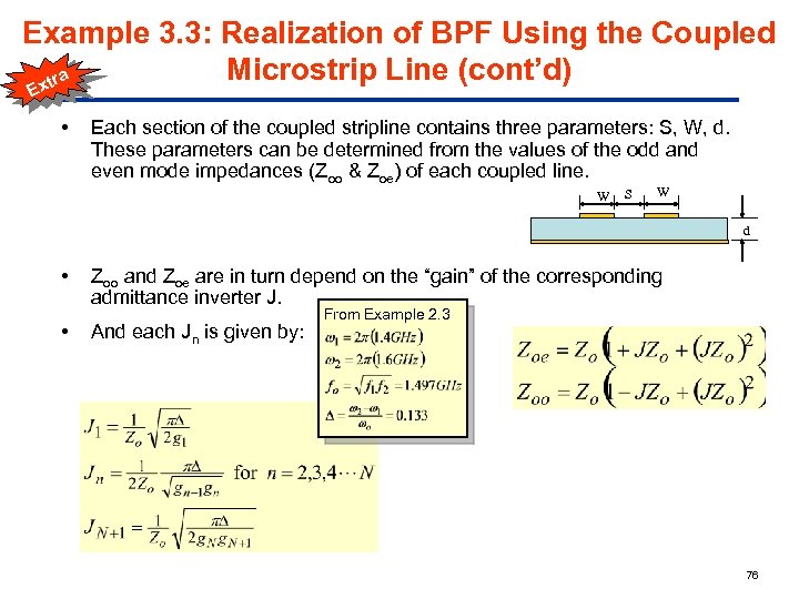 Example 3. 3: Realization of BPF Using the Coupled Microstrip Line (cont’d) a xtr E • Each section of the coupled stripline contains three parameters: S, W, d. These parameters can be determined from the values of the odd and even mode impedances (Zoo & Zoe) of each coupled line. W S W d • • Zoo and Zoe are in turn depend on the “gain” of the corresponding admittance inverter J. And each Jn is given by: From Example 2. 3 76
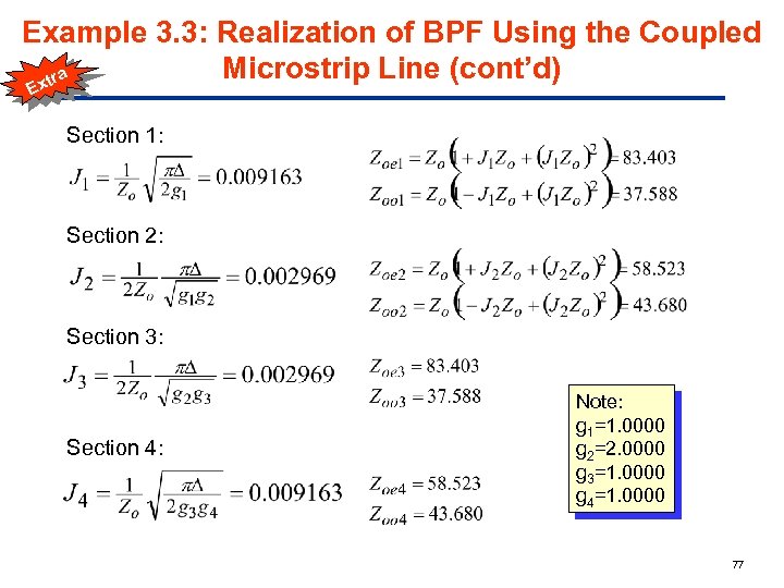 Example 3. 3: Realization of BPF Using the Coupled Microstrip Line (cont’d) a xtr E Section 1: Section 2: Section 3: Section 4: Note: g 1=1. 0000 g 2=2. 0000 g 3=1. 0000 g 4=1. 0000 77
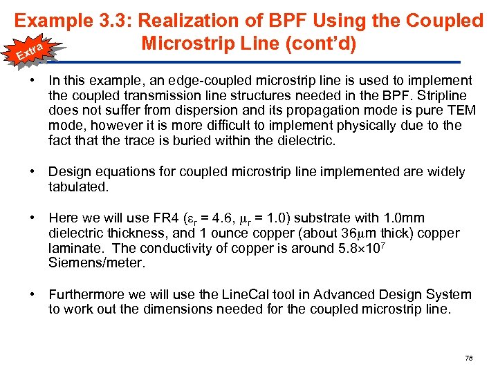 Example 3. 3: Realization of BPF Using the Coupled Microstrip Line (cont’d) a xtr E • In this example, an edge-coupled microstrip line is used to implement the coupled transmission line structures needed in the BPF. Stripline does not suffer from dispersion and its propagation mode is pure TEM mode, however it is more difficult to implement physically due to the fact that the trace is buried within the dielectric. • Design equations for coupled microstrip line implemented are widely tabulated. • Here we will use FR 4 ( r = 4. 6, r = 1. 0) substrate with 1. 0 mm dielectric thickness, and 1 ounce copper (about 36 m thick) copper laminate. The conductivity of copper is around 5. 8 107 Siemens/meter. • Furthermore we will use the Line. Cal tool in Advanced Design System to work out the dimensions needed for the coupled microstrip line. 78
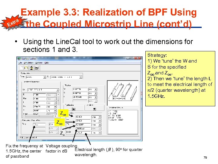 Example 3. 3: Realization of BPF Using a xtr E the Coupled Microstrip Line (cont’d) • Using the Line. Cal tool to work out the dimensions for sections 1 and 3. Strategy: 1) We ‘tune’ the W and S for the specified Zoo and Zoe. 2) Then we ‘tune’ the length L to meet the electrical length of /2 (quarter wavelength) at 1. 5 GHz. Zoe Zoo Zo Fix the frequency at Voltage coupling Electrical length ( l ), 90 o for quarter 1. 5 GHz, the center factor in d. B wavelength. of passband 79
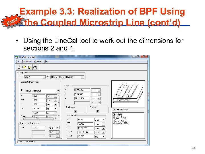 Example 3. 3: Realization of BPF Using a xtr E the Coupled Microstrip Line (cont’d) • Using the Line. Cal tool to work out the dimensions for sections 2 and 4. 80
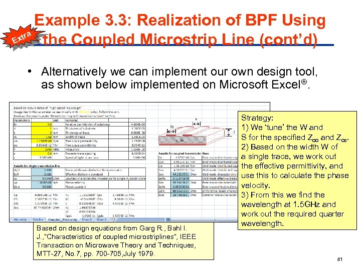 Example 3. 3: Realization of BPF Using a xtr E the Coupled Microstrip Line (cont’d) • Alternatively we can implement our own design tool, as shown below implemented on Microsoft Excel. Based on design equations from Garg R. , Bahl I. J. , ”Characteristics of coupled microstriplines”, IEEE Transaction on Microwave Theory and Techniques, MTT-27, No. 7, pp. 700 -705, July 1979. Strategy: 1) We ‘tune’ the W and S for the specified Zoo and Zoe. 2) Based on the width W of a single trace, we work out the effective permittivity, and use this to calculate the phase velocity. 3) From this we find the wavelength at 1. 5 GHz and work out the required quarter wavelength. 81
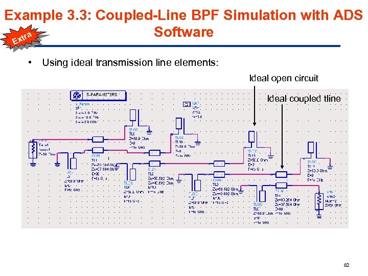 Example 3. 3: Coupled-Line BPF Simulation with ADS Software a xtr E • Using ideal transmission line elements: Ideal open circuit Ideal coupled tline 82
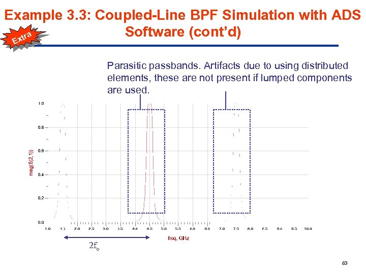 Example 3. 3: Coupled-Line BPF Simulation with ADS Software (cont’d) a xtr E Parasitic passbands. Artifacts due to using distributed elements, these are not present if lumped components are used. 2 fo 83
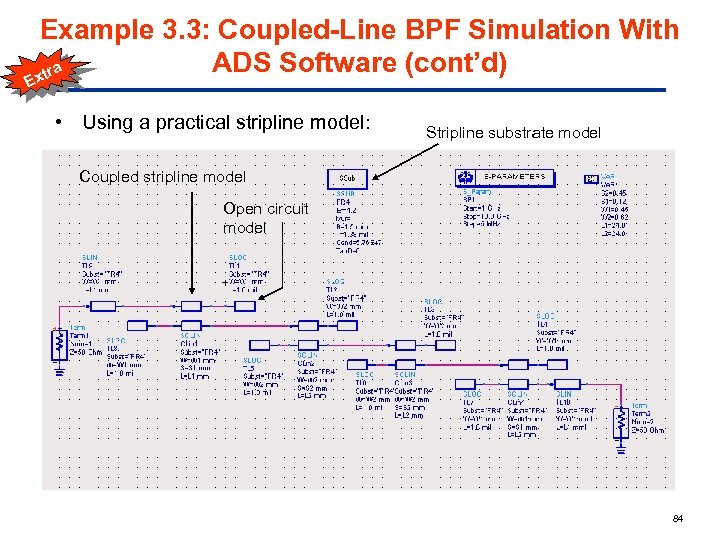 Example 3. 3: Coupled-Line BPF Simulation With ADS Software (cont’d) a xtr E • Using a practical stripline model: Stripline substrate model Coupled stripline model Open circuit model 84
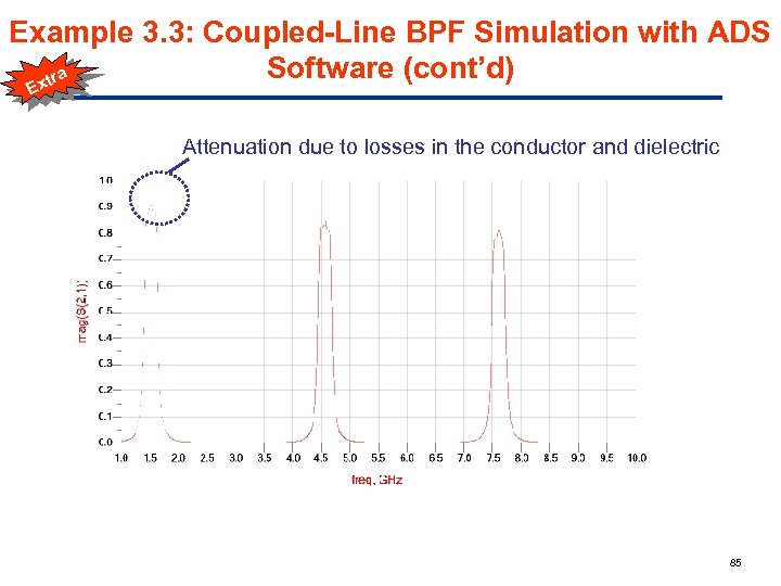 Example 3. 3: Coupled-Line BPF Simulation with ADS Software (cont’d) a xtr E Attenuation due to losses in the conductor and dielectric 85
 Items for Self-Study • Network analysis and realizability theory • Synthesis of terminated RLCM 1 -port circuits • Ideal impedance and admittance inverters and practical implementation • Periodic structures theory • Filter design by the Image Parameter Method (IPM). 86
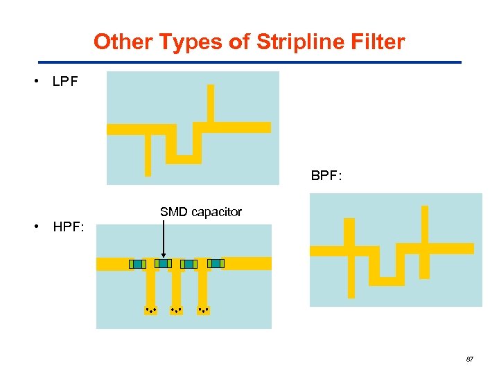 Other Types of Stripline Filter • LPF BPF: • HPF: SMD capacitor 87
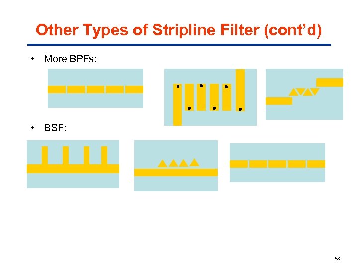 Other Types of Stripline Filter (cont’d) • More BPFs: • BSF: 88
 Appendix 1 – Kuroda’s Identities 89
![Kuroda’s Identities • As extracted from Ref. [2] l l Z 1 Z 2/n Kuroda’s Identities • As extracted from Ref. [2] l l Z 1 Z 2/n](https://present5.com/presentation/6fe71bb93ffa89464a6adf958053e08f/image-90.jpg) Kuroda’s Identities • As extracted from Ref. [2] l l Z 1 Z 2/n 2 n 2 Z 1 Z 2/n 2 1: n 2 l l Z 1 l l Z 2 Note: The length of all transmission lines is l = /8 l l Z 2 Note: The inductor represents the shorted Tline while the capacitor represents the open-circuit Tline. n 2 Z 1 n 2: 1 90
Kuroda’s Identities • As extracted from Ref. [2] l l Z 1 Z 2/n 2 n 2 Z 1 Z 2/n 2 1: n 2 l l Z 1 l l Z 2 Note: The length of all transmission lines is l = /8 l l Z 2 Note: The inductor represents the shorted Tline while the capacitor represents the open-circuit Tline. n 2 Z 1 n 2: 1 90
![References [1] R. E. Collin, “Foundations for Microwave Engineering”, 2 nd Edition 1992, Mc. References [1] R. E. Collin, “Foundations for Microwave Engineering”, 2 nd Edition 1992, Mc.](https://present5.com/presentation/6fe71bb93ffa89464a6adf958053e08f/image-91.jpg) References [1] R. E. Collin, “Foundations for Microwave Engineering”, 2 nd Edition 1992, Mc. Graw-Hill. [2] D. M. Pozar, “Microwave Engineering”, 2 nd Edition 1998, John-Wiley & Sons. * (3 rd Edition 2005, John-Wiley & Sons is now available) Other more advanced references: [3] W. Chen (Editor), “The Circuits and Filters Handbook”, 1995, CRC Press. * [4] I. Hunter, “Theory and Design of Microwave Filters”, 2001, The Institution of Electrical Engineers. * [5] G. Matthaei, L. Young, E. M. T. Jones, “Microwave Filters, Impedance. Matching Networks, and Coupling Structures”, 1980, Artech House. * [6] F. F. Kuo, “Network Analysis and Synthesis”, 2 nd Edition 1966, John. Wiley & Sons. * Recommended 91
References [1] R. E. Collin, “Foundations for Microwave Engineering”, 2 nd Edition 1992, Mc. Graw-Hill. [2] D. M. Pozar, “Microwave Engineering”, 2 nd Edition 1998, John-Wiley & Sons. * (3 rd Edition 2005, John-Wiley & Sons is now available) Other more advanced references: [3] W. Chen (Editor), “The Circuits and Filters Handbook”, 1995, CRC Press. * [4] I. Hunter, “Theory and Design of Microwave Filters”, 2001, The Institution of Electrical Engineers. * [5] G. Matthaei, L. Young, E. M. T. Jones, “Microwave Filters, Impedance. Matching Networks, and Coupling Structures”, 1980, Artech House. * [6] F. F. Kuo, “Network Analysis and Synthesis”, 2 nd Edition 1966, John. Wiley & Sons. * Recommended 91


