1028cc6c4b3ac7e4e26ce8f385fff4b1.ppt
- Количество слайдов: 16
 May 2003 doc. : IEEE 802. 15 -03/207 r 0 Project: IEEE P 802. 15 Working Group for Wireless Personal Area Networks (WPANs) Submission Title: [TG 3 a-Wisair contribution on multi band implementation] Date Submitted: [5 May, 2003] Source: [Gadi Shor] Company: [Wisair] Address: [24 Raoul Wallenberg st. Ramat Hachayal, Tel-Aviv, ISRAEL] Voice: [+972 -3 -7676605] FAX: [+972 -3 -6477608], E-Mail: [gadi. shor@wisair. com] Re: [802. 15. 3 a Call for proposal] Abstract: [Wisair’s contribution on multi band implementation issues] Purpose: [Response to questions from TG 3 a members] Notice: This document has been prepared to assist the IEEE P 802. 15. It is offered as a basis for discussion and is not binding on the contributing individual(s) or organization(s). The material in this document is subject to change in form and content after further study. The contributor(s) reserve(s) the right to add, amend or withdraw material contained herein. Release: The contributor acknowledges and accepts that this contribution becomes the property of IEEE and may be made publicly available by P 802. 15. Submission 1 Gadi Shor, Wisair
 May 2003 doc. : IEEE 802. 15 -03/207 r 0 Multi-Band Implementation Issues Submission Slide 2 Gadi Shor, Wisair
 May 2003 doc. : IEEE 802. 15 -03/207 r 0 Contents • Multi band generator - Requirements - Band Plan - Design example - Design considerations - Lo leakage Submission 3 Gadi Shor, Wisair
 May 2003 doc. : IEEE 802. 15 -03/207 r 0 Multi. Band Generator • Many possible architectures – Digital based – Analog Based – Combined approaches • Can be implemented using either Si. Ge or CMOS process • Low power consumption / Small die size Submission 4 Gadi Shor, Wisair
 May 2003 doc. : IEEE 802. 15 -03/207 r 0 Requirements • • • 3. 79 n. Sec between pulses in 132 Mpps Back to back pulses in 264 Mpps Better than 20 d. B in adjacent sub-band Better than 25 d. B in other sub-bands Rejection of out of band harmonics (To simplify UWB filter requirements) Submission 5 Gadi Shor, Wisair
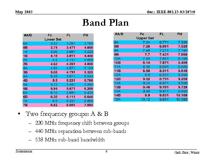 May 2003 doc. : IEEE 802. 15 -03/207 r 0 Band Plan • Two frequency groups: A & B – 220 MHz frequency shift between groups – 440 MHz separation between sub-bands – 538 MHz sub-bandwidth Submission 6 Gadi Shor, Wisair
 May 2003 doc. : IEEE 802. 15 -03/207 r 0 Design Example • Example of combined digital and analog implementation • Example is scalable with required pulse rate • Supports requirements for 132 Mpps and 264 Mpps • Covers lower set group A which allows up to 480 Mbps • To support group B additional division and multiplication is required • Future systems can use upper set with additional PLL and the same sub-band generator to support ~1 Gbps Submission 7 Gadi Shor, Wisair
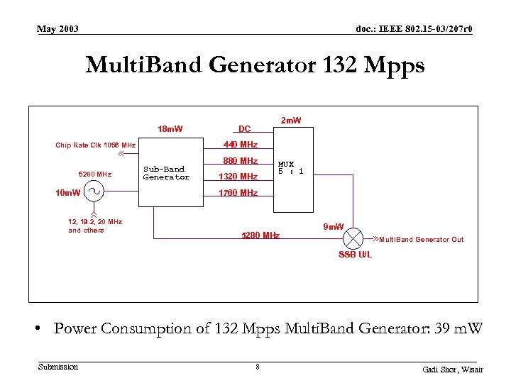 May 2003 doc. : IEEE 802. 15 -03/207 r 0 Multi. Band Generator 132 Mpps 18 m. W 440 MHz Chip Rate Clk 1056 MHz 5280 MHz 10 m. W 12, 19. 2, 20 MHz and others 2 m. W DC Sub-Band Generator 880 MHz 1320 MHz MUX 5 : 1 1760 MHz 5280 MHz 9 m. W Multi. Band Generator Out SSB U/L • Power Consumption of 132 Mpps Multi. Band Generator: 39 m. W Submission 8 Gadi Shor, Wisair
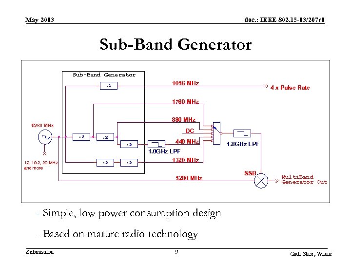 May 2003 doc. : IEEE 802. 15 -03/207 r 0 Sub-Band Generator 1056 MHz : 5 4 x Pulse Rate 1760 MHz 880 MHz 5280 MHz : 3 DC : 2 12, 19. 2, 20 MHz and more : 2 440 MHz 1. 8 GHz LPF 1. 0 GHz LPF 1320 MHz 5280 MHz SSB - Multi. Band Generator Out - Simple, low power consumption design - Based on mature radio technology Submission 9 Gadi Shor, Wisair
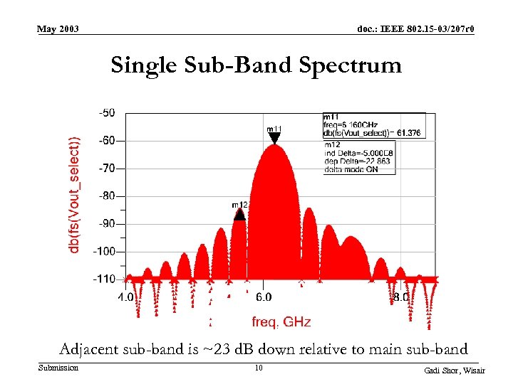 May 2003 doc. : IEEE 802. 15 -03/207 r 0 Single Sub-Band Spectrum Adjacent sub-band is ~23 d. B down relative to main sub-band Submission 10 Gadi Shor, Wisair
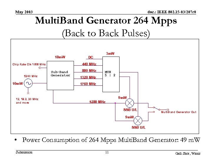 May 2003 doc. : IEEE 802. 15 -03/207 r 0 Multi. Band Generator 264 Mpps (Back to Back Pulses) 18 m. W 440 MHz Chip Rate Clk 1056 MHz 5280 MHz 10 m. W 12, 19. 2, 20 MHz and more 3 m. W DC Sub-Band Generator 880 MHz 1320 MHz MUX 5 : 2 1760 MHz 9 m. W 5280 MHz SSB U/L Multi. Band Generator Out 9 m. W SSB U/L • Power Consumption of 264 Mpps Multi. Band Generator: 49 m. W Submission 11 Gadi Shor, Wisair
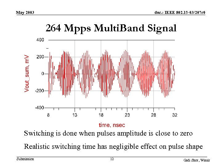 May 2003 doc. : IEEE 802. 15 -03/207 r 0 264 Mpps Multi. Band Signal Switching is done when pulses amplitude is close to zero Realistic switching time has negligible effect on pulse shape Submission 12 Gadi Shor, Wisair
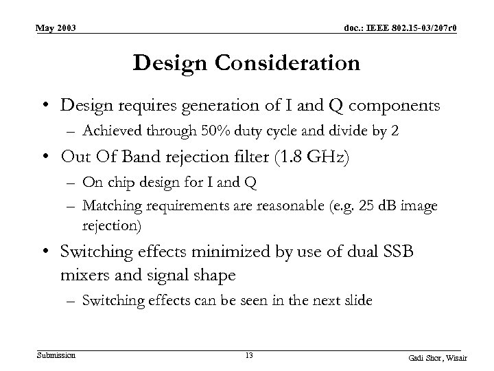 May 2003 doc. : IEEE 802. 15 -03/207 r 0 Design Consideration • Design requires generation of I and Q components – Achieved through 50% duty cycle and divide by 2 • Out Of Band rejection filter (1. 8 GHz) – On chip design for I and Q – Matching requirements are reasonable (e. g. 25 d. B image rejection) • Switching effects minimized by use of dual SSB mixers and signal shape – Switching effects can be seen in the next slide Submission 13 Gadi Shor, Wisair
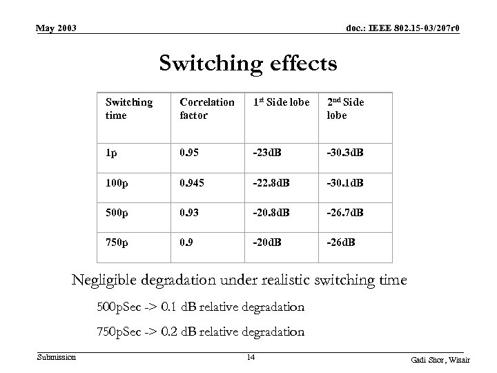 May 2003 doc. : IEEE 802. 15 -03/207 r 0 Switching effects Switching time Correlation factor 1 st Side lobe 2 nd Side lobe 1 p 0. 95 -23 d. B -30. 3 d. B 100 p 0. 945 -22. 8 d. B -30. 1 d. B 500 p 0. 93 -20. 8 d. B -26. 7 d. B 750 p 0. 9 -20 d. B -26 d. B Negligible degradation under realistic switching time 500 p. Sec -> 0. 1 d. B relative degradation 750 p. Sec -> 0. 2 d. B relative degradation Submission 14 Gadi Shor, Wisair
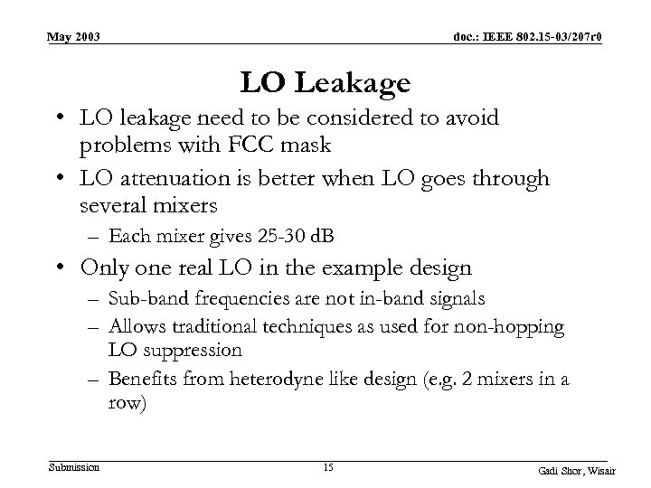 May 2003 doc. : IEEE 802. 15 -03/207 r 0 LO Leakage • LO leakage need to be considered to avoid problems with FCC mask • LO attenuation is better when LO goes through several mixers – Each mixer gives 25 -30 d. B • Only one real LO in the example design – Sub-band frequencies are not in-band signals – Allows traditional techniques as used for non-hopping LO suppression – Benefits from heterodyne like design (e. g. 2 mixers in a row) Submission 15 Gadi Shor, Wisair
 May 2003 doc. : IEEE 802. 15 -03/207 r 0 Summary • Multi band generator can be implemented in many ways • Requirements are set to allow reasonable implementation Submission 16 Gadi Shor, Wisair


