d065af75f62ad85a0228fc26a8edfa35.ppt
- Количество слайдов: 45
 MATERIALS FOR MEMS AND MICROSYSTEMS COURTESY MATERIAL FROM : TAI-RAN HSU “MEMS &MICROSYSTEMS BOOK
 Silicon – an ideal substrate material for MEMS ● Silicon (Si) is the most abundant material on earth. It almost always exists in compounds with other elements. ● Single crystal silicon is the most widely used substrate material for MEMS and microsystems. ● The popularity of silicon for such application is primarily for the following reasons: • It is mechanically stable and it is feasible to be integrated into electronics on the same substrate (b/c it is a semiconducting material). • Electronics for signal transduction such as the p or n-type piezoresistive can be readily integrated with the Si substrate-ideal for transistors. • Silicon is almost an ideal structure material. It has about the same Young’s modulus as steel ( 2 x 10⁵ MPa), but is as light as aluminum with a density of about 2. 3 g/cm 3.
 Silicon – an ideal substrate material for MEMS-Cont’d (4) It has a melting point at 1400 o. C, which is about twice higher than that of aluminum. This high melting point makes silicon dimensionally stable even at elevated temperature. (5) Its thermal expansion coefficient is about 8 times smaller than that of steel, and is more than 10 times smaller than that of aluminum. (6) Silicon shows virtually no mechanical hysteresis. It is thus an ideal candidate material for sensors and actuators. (7) Silicon wafers are extremely flat for coatings and additional thin film layers for either being integral structural parts, or performing precise electromechanical functions. (8) There is a greater flexibility in design and manufacture with silicon than with other substrate materials. Treatments and fabrication processes for silicon substrates are well established and documented.
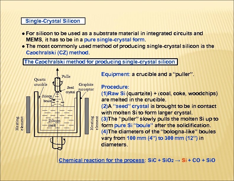 Single-Crystal Silicon ● For silicon to be used as a substrate material in integrated circuits and MEMS, it has to be in a pure single-crystal form. ● The most commonly used method of producing single-crystal silicon is the Czochralski (CZ) method. The Czochralski method for producing single-crystal silicon Pulle r Quartz crucible Equipment: a crucible and a “puller”. Graphite Seed susceptor crystal Silicon melt Heating element Silicon boule Procedure: (1)Raw Si (quartzite) + (coal, coke, woodchips) are melted in the crucible. (2)A “seed” crystal is brought to be in contact with molten Si to form larger crystal. (3)The “puller” slowly pulls the molten Si up to form pure Si “boule” after the solidification. (4)The diameters of the “bologna-like” boules vary from 100 mm (4”) to 300 mm (12”) in diameters. Chemical reaction for the process: Si. C + Si. O 2 → Si + CO + Si. O
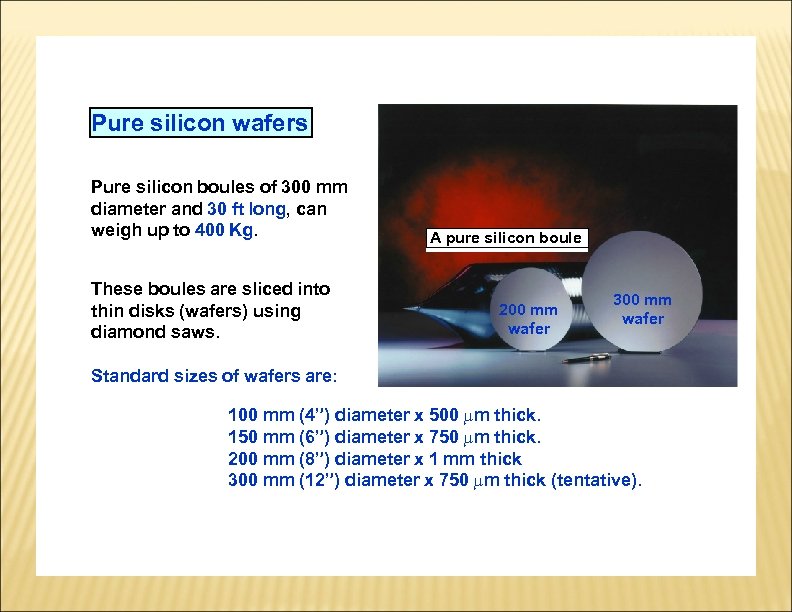 Pure silicon wafers Pure silicon boules of 300 mm diameter and 30 ft long, can weigh up to 400 Kg. These boules are sliced into thin disks (wafers) using diamond saws. A pure silicon boule 200 mm wafer 300 mm wafer Standard sizes of wafers are: 100 mm (4”) diameter x 500 m thick. 150 mm (6”) diameter x 750 m thick. 200 mm (8”) diameter x 1 mm thick 300 mm (12”) diameter x 750 m thick (tentative).
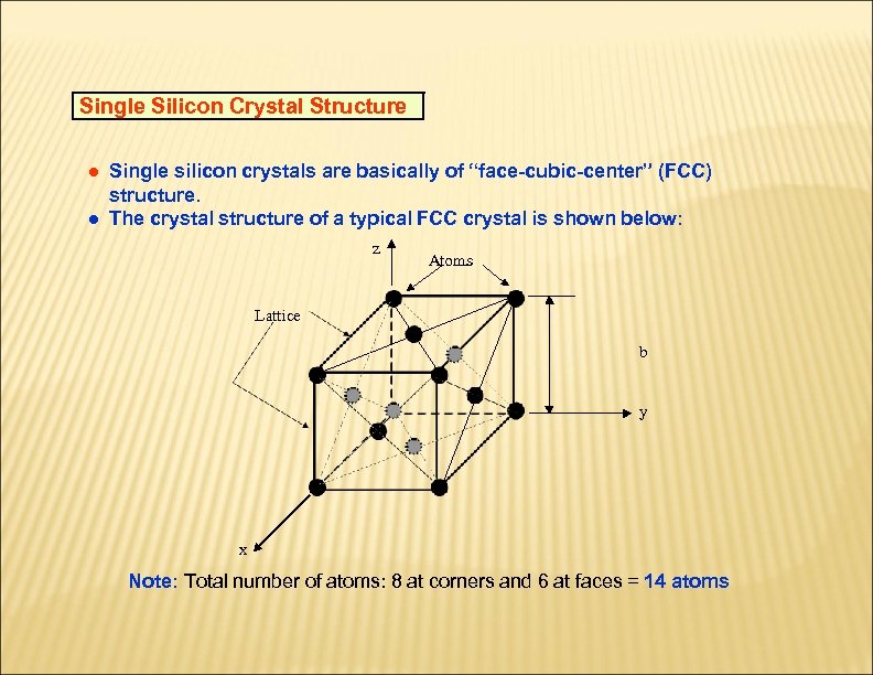 Single Silicon Crystal Structure ● Single silicon crystals are basically of “face-cubic-center” (FCC) structure. ● The crystal structure of a typical FCC crystal is shown below: z Atoms Lattice b y x Note: Total number of atoms: 8 at corners and 6 at faces = 14 atoms
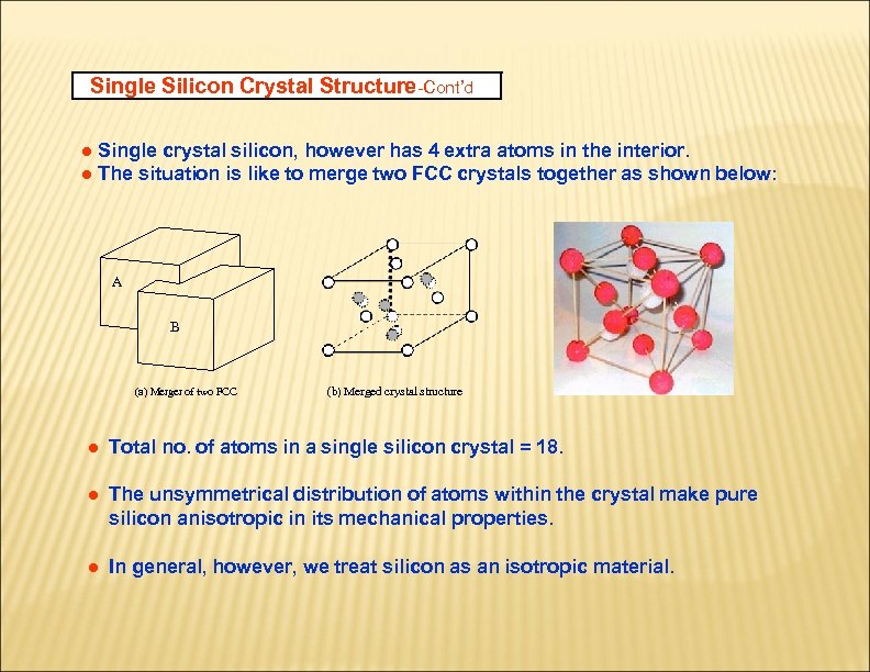 Single Silicon Crystal Structure-Cont’d ● Single crystal silicon, however has 4 extra atoms in the interior. ● The situation is like to merge two FCC crystals together as shown below: A B (a) Merger of two FCC (b) Merged crystal structure ● Total no. of atoms in a single silicon crystal = 18. ● The unsymmetrical distribution of atoms within the crystal make pure silicon anisotropic in its mechanical properties. ● In general, however, we treat silicon as an isotropic material.
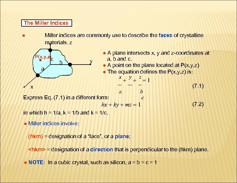 The Miller Indices ● Miller indices are commonly use to describe the faces of crystalline materials. z ● A plane intersects x, y and z-coordinates at a, b and c. c y b ● A point on the plane located at P(x, y, z) a ● The equation defines the P(x, y, z) is: x y z 1 (7. 1) x a b c Express Eq. (7. 1) in a different form: (7. 2) hx ky mz 1 P(x, y, z) in which h = 1/a, k = 1/b and k = 1/c. ● Miller indices involve: (hkm) = designation of a “face”, or a plane;
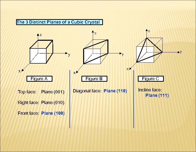 The 3 Distinct Planes of a Cubic Crystal z x x Figure A Top face: Plane (001) Right face: Plane (010) Front face: Plane (100) y y y x z z Figure B Diagonal face: Plane (110) Figure C Incline face: Plane (111)
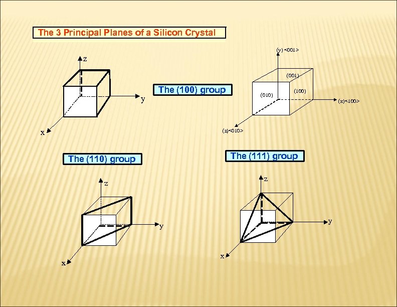 The 3 Principal Planes of a Silicon Crystal (y) <001> z (001) y The (100) group x (010) (100) (x)<100> (z)<010> The (111) group The (110) group z z y y x x
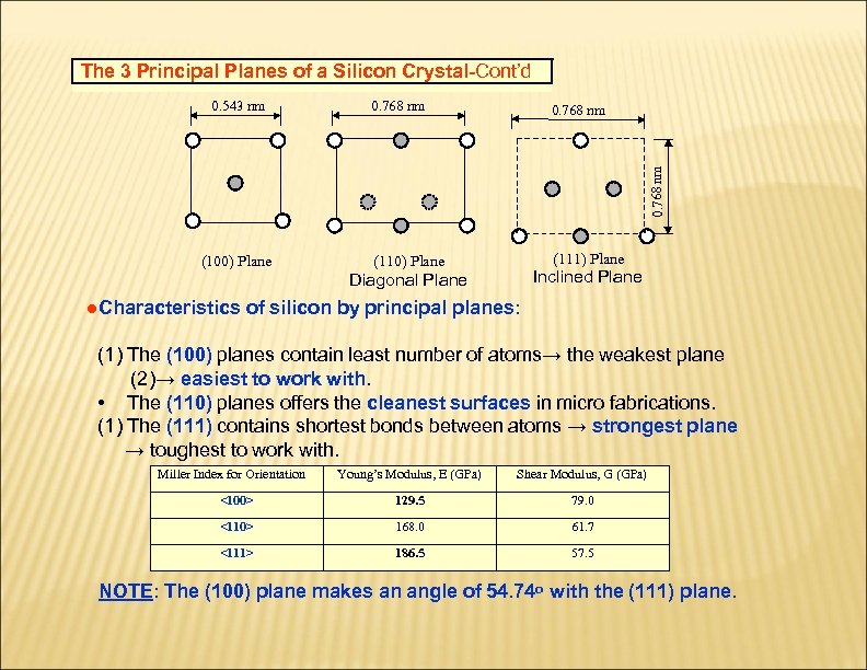 The 3 Principal Planes of a Silicon Crystal-Cont’d 0. 768 nm (110) Plane (111) Plane 0. 768 nm 0. 543 nm (100) Plane Inclined Plane Diagonal Plane ●Characteristics of silicon by principal planes: (1) The (100) planes contain least number of atoms→ the weakest plane (2)→ easiest to work with. • The (110) planes offers the cleanest surfaces in micro fabrications. (1) The (111) contains shortest bonds between atoms → strongest plane → toughest to work with. Miller Index for Orientation Young’s Modulus, E (GPa) Shear Modulus, G (GPa) <100> 129. 5 79. 0 <110> 168. 0 61. 7 <111> 186. 5 57. 5 NOTE: The (100) plane makes an angle of 54. 74 o with the (111) plane.
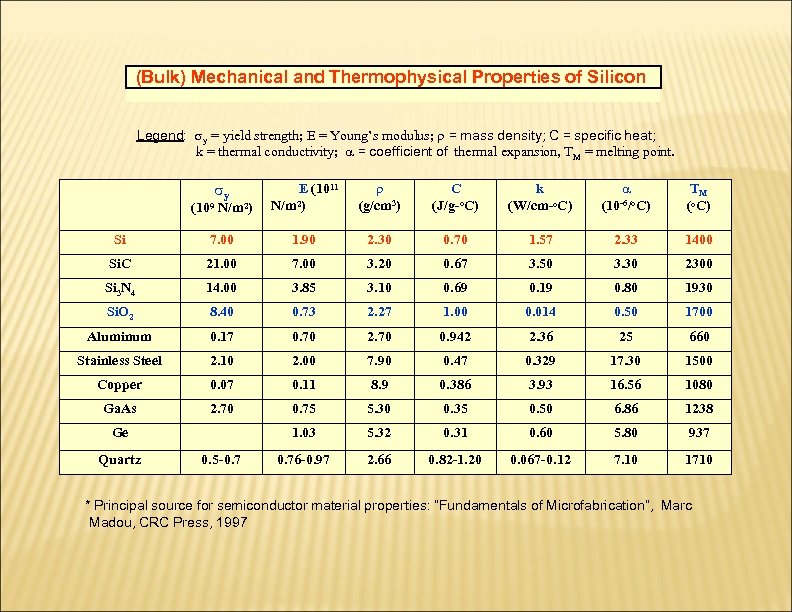 (Bulk) Mechanical and Thermophysical Properties of Silicon Legend: y = yield strength; E = Young’s modulus; = mass density; C = specific heat; k = thermal conductivity; = coefficient of thermal expansion, TM = melting point. y (109 N/m 2) E (1011 N/m 2) (g/cm 3) C (J/g-o. C) k (W/cm-o. C) (10 / C) TM (o. C) Si 7. 00 1. 90 2. 30 0. 70 1. 57 2. 33 1400 Si. C 21. 00 7. 00 3. 20 0. 67 3. 50 3. 30 2300 Si 3 N 4 14. 00 3. 85 3. 10 0. 69 0. 19 0. 80 1930 Si. O 2 8. 40 0. 73 2. 27 1. 00 0. 014 0. 50 1700 Aluminum 0. 17 0. 70 2. 70 0. 942 2. 36 25 660 Stainless Steel 2. 10 2. 00 7. 90 0. 47 0. 329 17. 30 1500 Copper 0. 07 0. 11 8. 9 0. 386 3. 93 16. 56 1080 Ga. As 2. 70 0. 75 5. 30 0. 35 0. 50 6. 86 1238 1. 03 5. 32 0. 31 0. 60 5. 80 937 0. 76 -0. 97 2. 66 0. 82 -1. 20 0. 067 -0. 12 7. 10 1710 Ge Quartz 0. 5 -0. 7 -6 o * Principal source for semiconductor material properties: “Fundamentals of Microfabrication”, Marc Madou, CRC Press, 1997
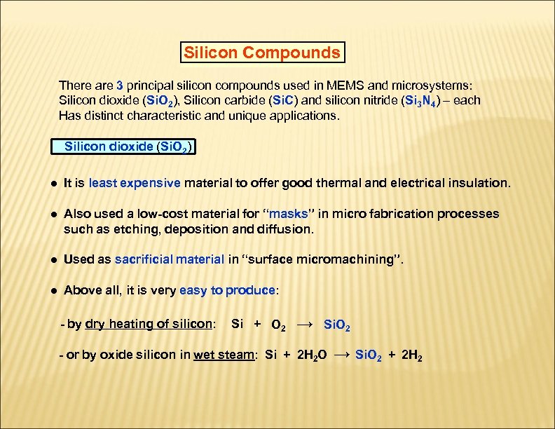 Silicon Compounds There are 3 principal silicon compounds used in MEMS and microsystems: Silicon dioxide (Si. O 2), Silicon carbide (Si. C) and silicon nitride (Si 3 N 4) – each Has distinct characteristic and unique applications. Silicon dioxide (Si. O 2) ● It is least expensive material to offer good thermal and electrical insulation. ● Also used a low-cost material for “masks” in micro fabrication processes such as etching, deposition and diffusion. ● Used as sacrificial material in “surface micromachining”. ● Above all, it is very easy to produce: - by dry heating of silicon: Si + O 2 → Si. O 2 - or by oxide silicon in wet steam: Si + 2 H 2 O → Si. O 2 + 2 H 2
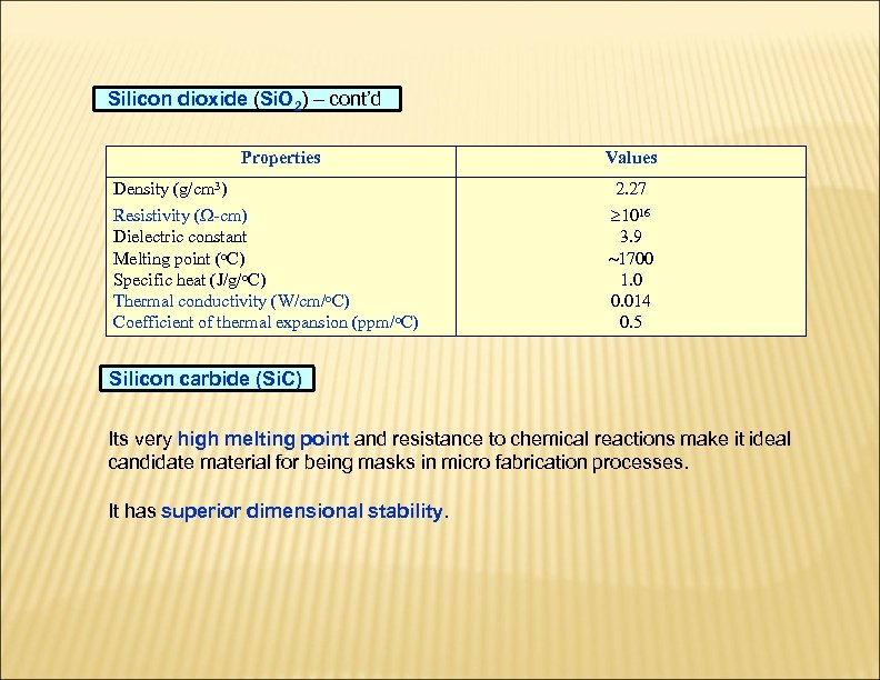 Silicon dioxide (Si. O 2) – cont’d Properties Density (g/cm 3) Resistivity ( -cm) Dielectric constant Melting point (o. C) Specific heat (J/g/o. C) Thermal conductivity (W/cm/o. C) Coefficient of thermal expansion (ppm/o. C) Values 2. 27 1016 3. 9 1700 1. 0 0. 014 0. 5 Silicon carbide (Si. C) Its very high melting point and resistance to chemical reactions make it ideal candidate material for being masks in micro fabrication processes. It has superior dimensional stability.
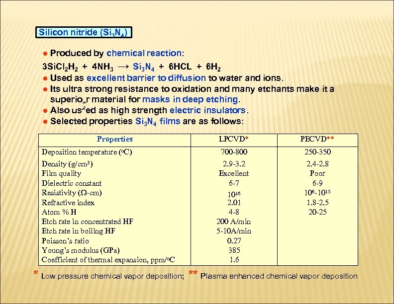 Silicon nitride (Si 3 N 4) ● Produced by chemical reaction: 3 Si. Cl 2 H 2 + 4 NH 3 → Si 3 N 4 + 6 HCL + 6 H 2 ● Used as excellent barrier to diffusion to water and ions. ● Its ultra strong resistance to oxidation and many etchants make it a superio r material for masks in deep etching. ● Also us. Aed as high strength electric insulators. ● Selected properties Si 3 N 4 films are as follows: oo Properties Deposition temperature (o. C) Density (g/cm 3) Film quality Dielectric constant Resistivity ( -cm) Refractive index Atom % H Etch rate in concentrated HF Etch rate in boillng HF Poisson’s ratio Young’s modulus (GPa) Coefficient of thermal expansion, ppm/o. C LPCVD* PECVD** 700 -800 2. 9 -3. 2 Excellent 6 -7 1016 2. 01 4 -8 200 A/min 5 -10 A/min 0. 27 385 1. 6 250 -350 2. 4 -2. 8 Poor 6 -9 106 -1015 1. 8 -2. 5 20 -25 * Low pressure chemical vapor deposition; ** Plasma enhanced chemical vapor deposition
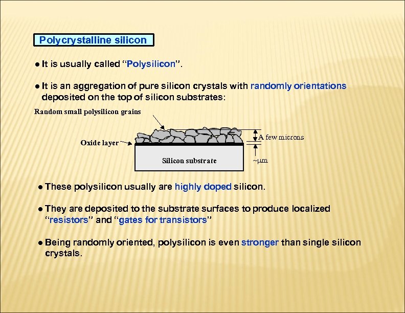 Polycrystalline silicon ● It is usually called “Polysilicon”. ● It is an aggregation of pure silicon crystals with randomly orientations deposited on the top of silicon substrates: Random small polysilicon grains A few microns Oxide layer Silicon substrate m ● These polysilicon usually are highly doped silicon. ● They are deposited to the substrate surfaces to produce localized “resistors” and “gates for transistors” ● Being randomly oriented, polysilicon is even stronger than single silicon crystals.
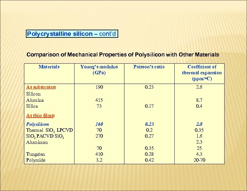 Polycrystalline silicon – cont’d Comparison of Mechanical Properties of Polysilicon with Other Materials As substrates: Silicon Alumina Silica Young’s modulus (GPa) Poisson’s ratio Coefficient of thermal expansion (ppm/o. C) 190 0. 23 2. 6 415 73 0. 17 8. 7 0. 4 160 70 270 0. 23 0. 27 70 410 3. 2 0. 35 0. 28 0. 42 As thin films: Polysilicon Thermal Si. O 2 LPCVD Si. O 2 PACVD Si. O 2 Aluminum Tungsten Polymide 2. 8 0. 35 1. 6 2. 3 25 4. 3 20 -70
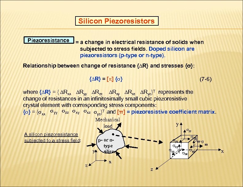 Silicon Piezoresistors Piezoresistance = a change in electrical resistance of solids when subjected to stress fields. Doped silicon are piezoresistors (p-type or n-type). Relationship between change of resistance {∆R} and stresses {σ}: { R} = [ ] { } (7 -6) where { R} = { Rxx Ryy Rzz Rxy Rxz Ryz}T represents the change of resistances in an infinitesimally small cubic piezoresistive crystal element with corresponding stress components: { } = { xx yy zz xy xz yz}T and [π] = piezoresistive coefficient matrix. Mechanical load A silicon piezoresistance subjected to a stress field: y yx xy yz zy p- or ntype y silicon z yy zz x z zx xz xx x
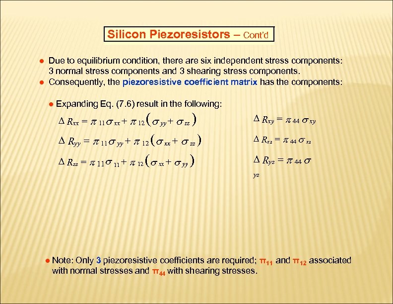 Silicon Piezoresistors – Cont’d ● Due to equilibrium condition, there are six independent stress components: 3 normal stress components and 3 shearing stress components. ● Consequently, the piezoresistive coefficient matrix has the components: ● Expanding Eq. (7. 6) result in the following: Rxx 11 xx 12 yy zz Rxy 44 xy Ryy 11 yy 12 xx zz Rxz 44 xz Rzz 11 11 12 xx yy Ryz 44 yz ● Note: Only 3 piezoresistive coefficients are required; π11 and π12 associated with normal stresses and π44 with shearing stresses.
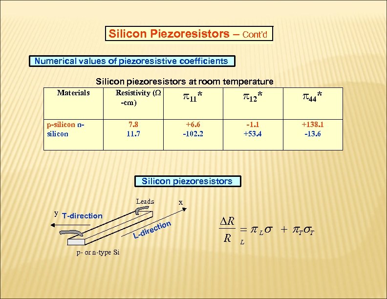 Silicon Piezoresistors – Cont’d Numerical values of piezoresistive coefficients Silicon piezoresistors at room temperature Materials 11* p-silicon nsilicon 7. 8 11. 7 12* 44* +6. 6 -102. 2 Resistivity ( -cm) -1. 1 +53. 4 +138. 1 -13. 6 Silicon piezoresistors Leads y T-direction ir L-d n ctio e p- or n-type Si x R L T T R L
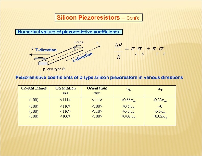 Silicon Piezoresistors – Cont’d Numerical values of piezoresistive coefficients Leads y T-direction x ion ect -dir L R L R L T T p- or n-type Si Piezoresistive coefficients of p-type silicon piezorestors in various directions Crystal Planes Orientation
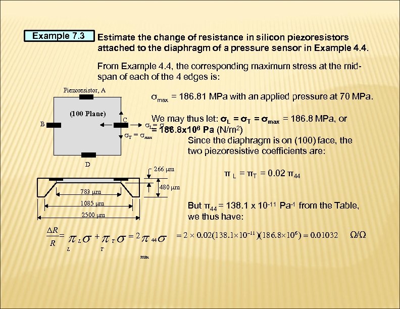 Example 7. 3 Estimate the change of resistance in silicon piezoresistors attached to the diaphragm of a pressure sensor in Example 4. 4. From Example 4. 4, the corresponding maximum stress at the midspan of each of the 4 edges is: Piezoresistor, A σmax = 186. 81 MPa with an applied pressure at 70 MPa. (100 Plane) We may thus let: σL = σT = σmax = 186. 8 MPa, or = 186. 8 x 10⁶ Pa (N/m 2) T = max Since the diaphragm is on (100) face, the two piezoresistive coefficients are: C B L = max D 266 m 480 m 783 m 1085 m But π44 = 138. 1 x 10 -11 Pa-1 from the Table, we thus have: 2500 m R R L L π L = πT = 0. 02 π44 T 2 44 T max 2 0. 02(138. 1 10 11 )(186. 8 106 ) 0. 01032 Ω/Ω
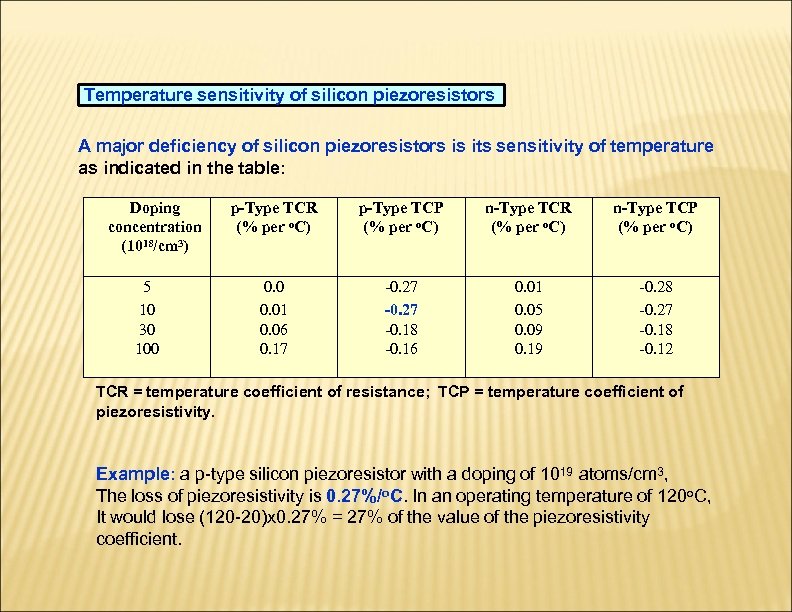 Temperature sensitivity of silicon piezoresistors A major deficiency of silicon piezoresistors is its sensitivity of temperature as indicated in the table: Doping concentration (1018/cm 3) 5 10 30 100 p-Type TCR (% per o. C) p-Type TCP (% per o. C) n-Type TCR (% per o. C) n-Type TCP (% per o. C) 0. 01 0. 06 0. 17 -0. 27 -0. 18 -0. 16 0. 01 0. 05 0. 09 0. 19 -0. 28 -0. 27 -0. 18 -0. 12 TCR = temperature coefficient of resistance; TCP = temperature coefficient of piezoresistivity. Example: a p-type silicon piezoresistor with a doping of 1019 atoms/cm 3, The loss of piezoresistivity is 0. 27%/o. C. In an operating temperature of 120 o. C, It would lose (120 -20)x 0. 27% = 27% of the value of the piezoresistivity coefficient.
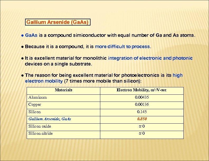 Gallium Arsenide (Ga. As) ● Ga. As is a compound simiconductor with equal number of Ga and As atoms. ● Because it is a compound, it is more difficult to process. ● It is excellent material for monolithic integration of electronic and photonic devices on a single substrate. ● The reason for being excellent material for photoelectronics is its high electron mobility (7 times more mobile than silicon): Materials Electron Mobility, m 2/V-sec Aluminum 0. 00435 Copper 0. 00136 Silicon 0. 145 Gallium Arsenide, Ga. As 0. 850 Silicon oxide 0 Silicon nitride 0
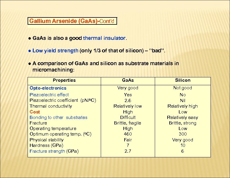 Gallium Arsenide (Ga. As)-Cont’d ● Ga. As is also a good thermal insulator. ● Low yield strength (only 1/3 of that of silicon) – “bad”. ● A comparison of Ga. As and silicon as substrate materials in micromachining: Properties Opto-electronics Piezoelectric effect Piezoelectric coefficient (p. N/o. C) Thermal conductivity Cost Bonding to other substrates Fracture Operating temperature Optimum operating temp. (o. C) Physical stability Hardness (GPa) Fracture strength (GPa) Ga. As Silicon Very good Yes 2. 6 Relatively low High Difficult Brittle, fragile High 460 Fair 7 2. 7 Not good No Nil Relatively high Low Relatively easy Brittle, strong Low 300 Very good 10 6
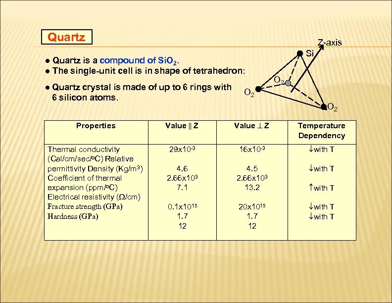 Quartz Z-axis ● Quartz is a compound of Si. O 2. ● The single-unit cell is in shape of tetrahedron: ● Quartz crystal is made of up to 6 rings with 6 silicon atoms. Si O 2 O 2 Properties Value Z Temperature Dependency Thermal conductivity (Cal/cm/sec/o. C) Relative permittivity Density (Kg/m 3) Coefficient of thermal expansion (ppm/o. C) Electrical resistivity ( /cm) Fracture strength (GPa) Hardness (GPa) 29 x 10 -3 16 x 10 -3 with T 4. 6 2. 66 x 103 7. 1 4. 5 2. 66 x 103 13. 2 with T 0. 1 x 10¹⁵ 1. 7 12 20 x 1015 1. 7 12 with T
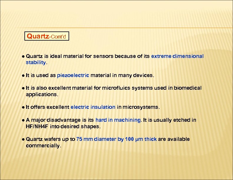 Quartz-Cont’d ● Quartz is ideal material for sensors because of its extreme dimensional stability. ● It is used as piezoelectric material in many devices. ● It is also excellent material for microfluics systems used in biomedical applications. ● It offers excellent electric insulation in microsystems. ● A major disadvantage is its hard in machining. It is usually etched in HF/NH 4 F into desired shapes. ● Quartz wafers up to 75 mm diameter by 100 µm thick are available commercially.
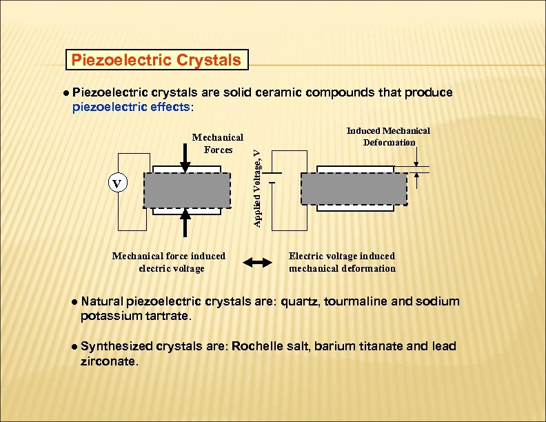 Piezoelectric Crystals ● Piezoelectric crystals are solid ceramic compounds that produce piezoelectric effects: V Mechanical force induced electric voltage Induced Mechanical Deformation Applied Voltage, V Mechanical Forces Electric voltage induced mechanical deformation ● Natural piezoelectric crystals are: quartz, tourmaline and sodium potassium tartrate. ● Synthesized crystals are: Rochelle salt, barium titanate and lead zirconate.
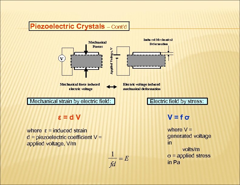 Piezoelectric Crystals – Cont’d V Induced Mechanical Deformation Applied Voltage, V Mechanical Forces Mechanical force induced electric voltage Electric voltage induced mechanical deformation Mechanical strain by electric field: ε=d. V Electric field by stress: V=fσ where ε = induced strain d = piezoelectric coefficient V = applied voltage, V/m 1 E fd where V = generated voltage in volts/m σ = applied stress in Pa
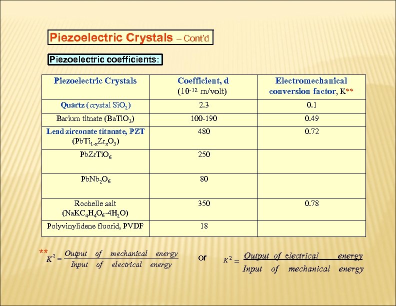 Piezoelectric Crystals – Cont’d Piezoelectric coefficients: Piezoelectric Crystals Coefficient, d (10 -12 m/volt) Electromechanical conversion factor, K** Quartz (crystal Si. O 2) 2. 3 0. 1 Barium titnate (Ba. Ti. O 3) 100 -190 0. 49 Lead zirconate titanate, PZT (Pb. Ti 1 -x. Zrx. O 3) 480 0. 72 Pb. Zr. Ti. O 6 250 Pb. Nb 2 O 6 80 Rochelle salt (Na. KC 4 H 4 O 6 -4 H 2 O) 350 Polyvinylidene fluorid, PVDF 18 **K 2 Output of Input of mechanical energy electrical energy or 0. 78 K 2 Output of electrical energy Input of mechanical energy
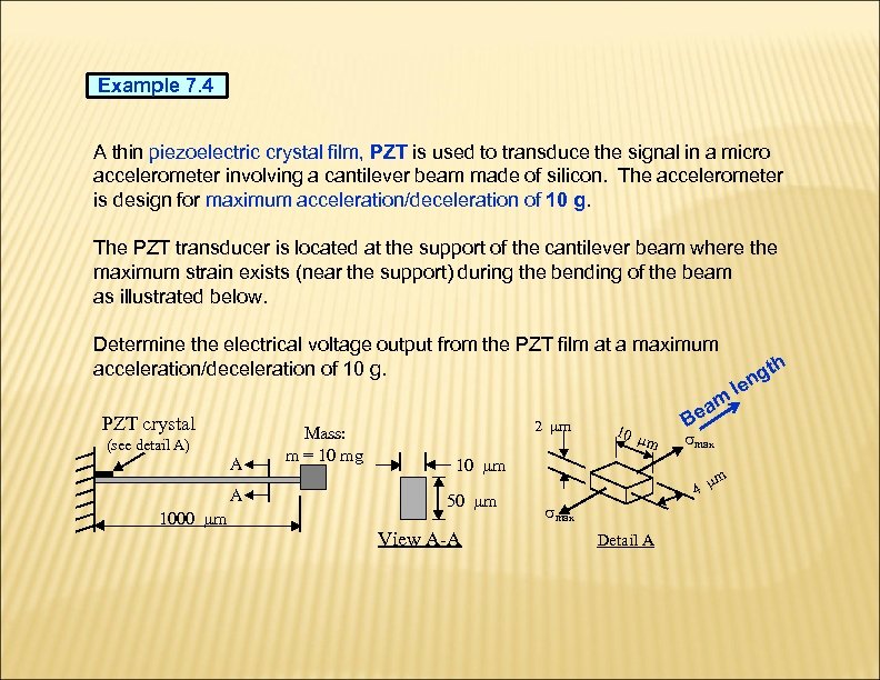 Example 7. 4 A thin piezoelectric crystal film, PZT is used to transduce the signal in a micro accelerometer involving a cantilever beam made of silicon. The accelerometer is design for maximum acceleration/deceleration of 10 g. The PZT transducer is located at the support of the cantilever beam where the maximum strain exists (near the support) during the bending of the beam as illustrated below. Determine the electrical voltage output from the PZT film at a maximum acceleration/deceleration of 10 g. PZT crystal (see detail A) A A 1000 m Mass: m = 10 mg 2 m am 10 m Be max 10 m 50 m View A-A 4 max Detail A m le gth n
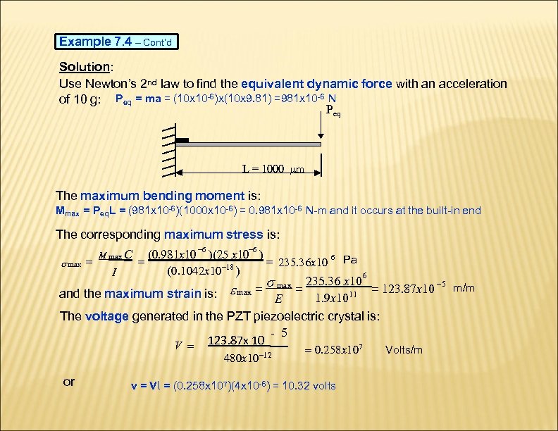 Example 7. 4 – Cont’d Solution: Use Newton’s 2 nd law to find the equivalent dynamic force with an acceleration of 10 g: Peq = ma = (10 x 10 -6)x(10 x 9. 81) =981 x 10 -6 N Peq L = 1000 m The maximum bending moment is: Mmax = Peq. L = (981 x 10 -6)(1000 x 10 -6) = 0. 981 x 10 -6 N-m and it occurs at the built-in end The corresponding maximum stress is: M max C 6 6 (0. 981 x 10 )(25 x 10 ) 235. 36 x 10 6 Pa max 18 (0. 1042 x 10 ) I 6 max 235. 36 x 10 123. 87 x 10 5 m/m and the maximum strain is: max E 1. 9 x 10¹¹ The voltage generated in the PZT piezoelectric crystal is: - 5 123. 87 x 10 7 V 480 x 10 12 or 0. 258 x 10 v = Vl = (0. 258 x 107)(4 x 10 -6) = 10. 32 volts Volts/m
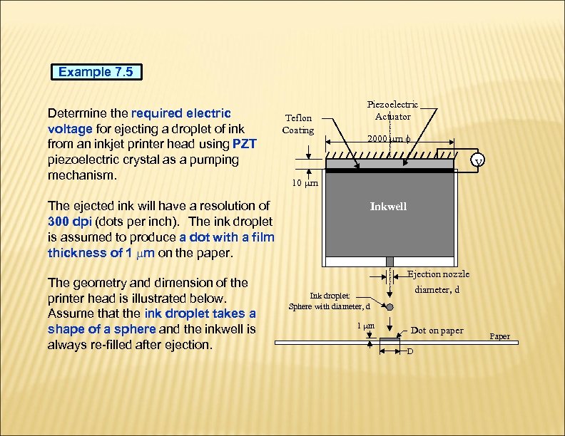 Example 7. 5 Determine the required electric voltage for ejecting a droplet of ink from an inkjet printer head using PZT piezoelectric crystal as a pumping mechanism. The ejected ink will have a resolution of 300 dpi (dots per inch). The ink droplet is assumed to produce a dot with a film thickness of 1 m on the paper. The geometry and dimension of the printer head is illustrated below. Assume that the ink droplet takes a shape of a sphere and the inkwell is always re-filled after ejection. Teflon Coating Piezoelectric Actuator 2000 m V 10 m Inkwell Ejection nozzle diameter, d Ink droplet: Sphere with diameter, d 1 m Dot on paper D Paper
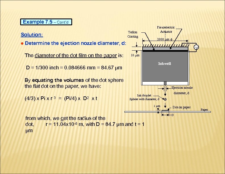 Example 7. 5 – Cont’d Solution: Teflon Coating ● Determine the ejection nozzle diameter, d: Piezoelectric Actuator 2000 m V The diameter of the dot film on the paper is: 10 m Inkwell D = 1/300 inch = 0. 084666 mm = 84. 67 µm By equating the volumes of the dot sphere the flat dot on the paper, we have: (4/3) x Pi x r 3 = (Pi/4) x D 2 x t Ejection nozzle diameter, d Ink droplet: Sphere with diameter, d 1 m from which, we get the radius of the dot, r = 11. 04 x 10 -6 m, with D = 84. 7 µm and t = 1 µm Dot on paper D Paper
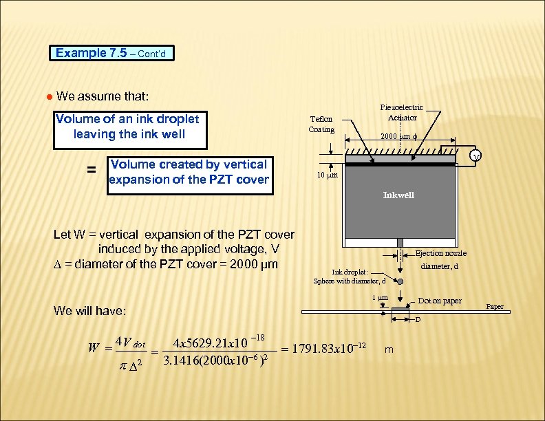 Example 7. 5 – Cont’d ● We assume that: Volume of an ink droplet leaving the ink well = Teflon Coating Piezoelectric Actuator 2000 m V Volume created by vertical expansion of the PZT cover 10 m Inkwell Let W = vertical expansion of the PZT cover induced by the applied voltage, V ∆ = diameter of the PZT cover = 2000 µm Ejection nozzle 1 m We will have: 18 4 V dot 4 x 5629. 21 x 10 W 3. 1416(2000 x 10 6 )2 2 diameter, d Ink droplet: Sphere with diameter, d Dot on paper D 1791. 83 x 10 12 m Paper
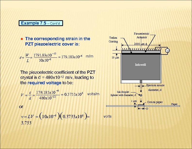 Example 7. 5 – Cont’d ● The corresponding strain in the PZT piezoelectric cover is: W 1791. 83 x 10 6 L 12 10 x 10 Teflon Coating Piezoelectric Actuator 2000 m V 179. 183 x 10 6 m/m 10 m Inkwell The piezoelectric coefficient of the PZT crystal is d = 480 x 10 -12 m/v, leading to the required voltage to be: 179. 183 x 10 V 480 x 10 12 d 6 0. 3733 x 10 6 volts/m Ejection nozzle 1 m or v LV 10 x 10 6 3. 733 0. 3733 x 10 6 diameter, d Ink droplet: Sphere with diameter, d Dot on paper D volts Paper
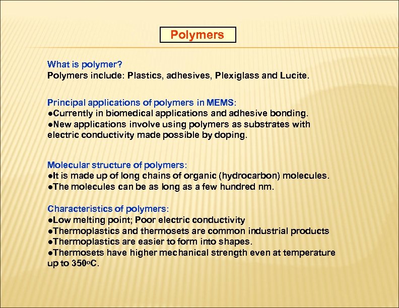 Polymers What is polymer? Polymers include: Plastics, adhesives, Plexiglass and Lucite. Principal applications of polymers in MEMS: ●Currently in biomedical applications and adhesive bonding. ●New applications involve using polymers as substrates with electric conductivity made possible by doping. Molecular structure of polymers: ●It is made up of long chains of organic (hydrocarbon) molecules. ●The molecules can be as long as a few hundred nm. Characteristics of polymers: ●Low melting point; Poor electric conductivity ●Thermoplastics and thermosets are common industrial products ●Thermoplastics are easier to form into shapes. ●Thermosets have higher mechanical strength even at temperature up to 350 o. C.
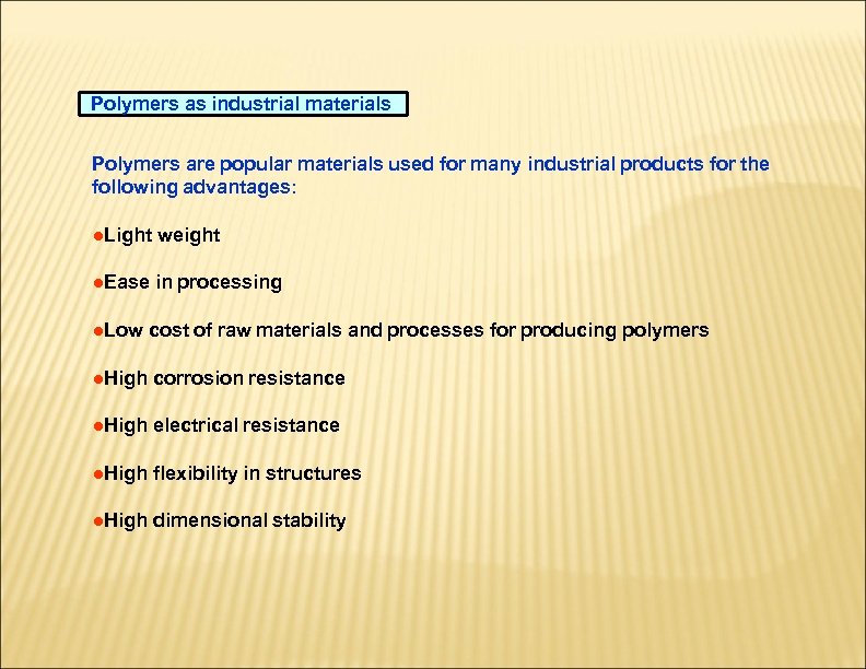 Polymers as industrial materials Polymers are popular materials used for many industrial products for the following advantages: ●Light weight ●Ease in processing ●Low cost of raw materials and processes for producing polymers ●High corrosion resistance ●High electrical resistance ●High flexibility in structures ●High dimensional stability
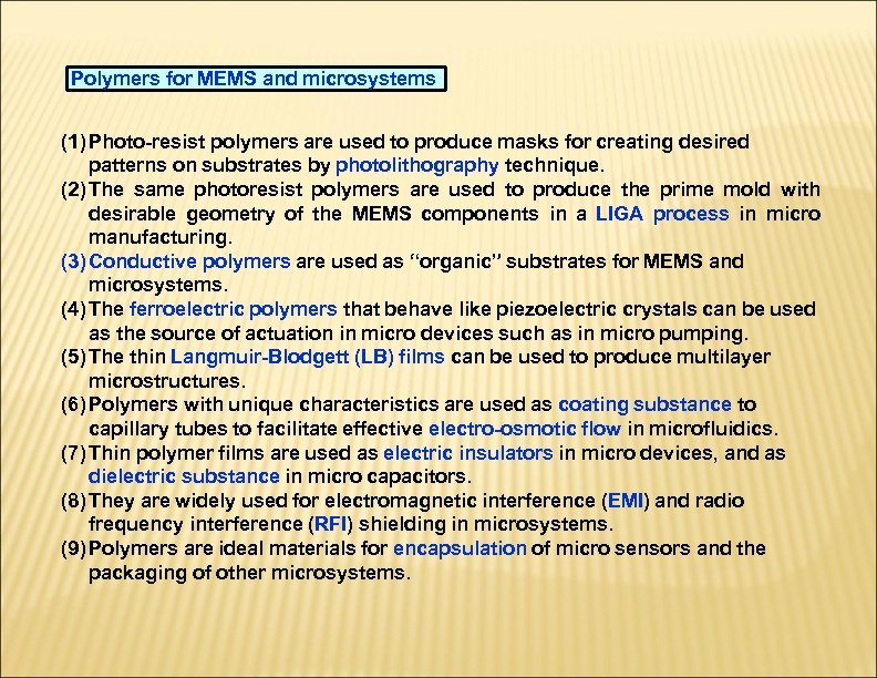 Polymers for MEMS and microsystems (1) Photo-resist polymers are used to produce masks for creating desired patterns on substrates by photolithography technique. (2) The same photoresist polymers are used to produce the prime mold with desirable geometry of the MEMS components in a LIGA process in micro manufacturing. (3) Conductive polymers are used as “organic” substrates for MEMS and microsystems. (4) The ferroelectric polymers that behave like piezoelectric crystals can be used as the source of actuation in micro devices such as in micro pumping. (5) The thin Langmuir-Blodgett (LB) films can be used to produce multilayer microstructures. (6) Polymers with unique characteristics are used as coating substance to capillary tubes to facilitate effective electro-osmotic flow in microfluidics. (7) Thin polymer films are used as electric insulators in micro devices, and as dielectric substance in micro capacitors. (8) They are widely used for electromagnetic interference (EMI) and radio frequency interference (RFI) shielding in microsystems. (9) Polymers are ideal materials for encapsulation of micro sensors and the packaging of other microsystems.
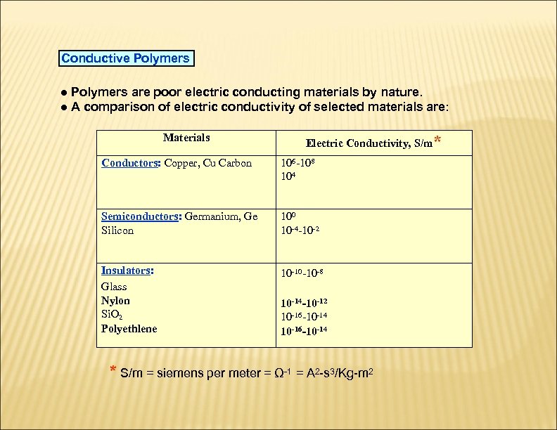 Conductive Polymers ● Polymers are poor electric conducting materials by nature. ● A comparison of electric conductivity of selected materials are: Materials Electric Conductivity, S/m* Conductors: Copper, Cu Carbon 106 -108 104 Semiconductors: Germanium, Ge Silicon 100 10 -4 -10 -2 Insulators: Glass Nylon Si. O 2 Polyethlene 10 -10 -10 -8 10 -14 -10 -12 10 -16 -10 -14 * S/m = siemens per meter = Ω-1 = A 2 -s 3/Kg-m 2
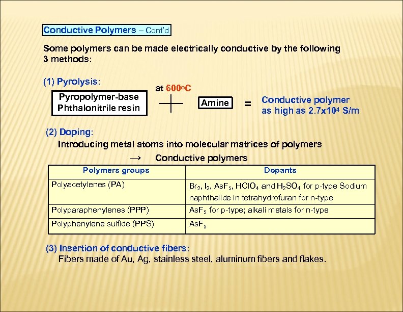 Conductive Polymers – Cont’d Some polymers can be made electrically conductive by the following 3 methods: (1) Pyrolysis: Pyropolymer-base Phthalonitrile resin at 600 o. C Amine = Conductive polymer as high as 2. 7 x 10⁴ S/m (2) Doping: Introducing metal atoms into molecular matrices of polymers → Conductive polymers Polymers groups Polyacetylenes (PA) Dopants Polyparaphenylenes (PPP) Br 2, I 2, As. F 5, HCl. O 4 and H 2 SO 4 for p-type Sodium naphthalide in tetrahydrofuran for n-type As. F 5 for p-type; alkali metals for n-type Polyphenylene sulfide (PPS) As. F 5 (3) Insertion of conductive fibers: Fibers made of Au, Ag, stainless steel, aluminum fibers and flakes.
 Langmuir-Blodgett (LB) films ● The process was first introduced by Langmuir in 1917 and was later refined by Blodgett. That was why it is called Langmuir-Blodgett process, or LB films. ● The process involves the spreading volatile solvent over the surface-active substrate materials. ● The LB process can produce more than one single monolayer by depositing films of various compositions onto a substrate to produce a multilayer structure. ● LB films are good candidate materials for exhibiting ferro (iron)- , pyro (heat)and piezoelectric properties. LB films may also be produced with controlled optical properties such as refractive index and anti reflections. They are thus ideal materials for micro sensors and optoelectronic devices.
 Langmuir-Blodgett (LB) films – Cont’d ● Following are a few examples of LB film applications in microsystems: • Ferroelectric (magnetic) polymer thin films: ● The one in particular is the Poly-vinylidene fluoride (PVDF). ● Applications of this type of films include: - Sound transducers in air and water, - Tactile sensors, - Biomedical applications such as tissue compatibility, cardiopulmonary sensors and implantable transducers and sensors for prosthetics and rehabilitation devices. ● As a piezoelectric source. The piezoelectric coefficient of PVDF is given in Table 7 -14. • Coating materials with controllable optical properties: ● Broadband optical fibers that transmit light at various wavelengths.
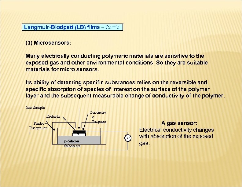 Langmuir-Blodgett (LB) films – Cont’d (3) Microsensors: Many electrically conducting polymeric materials are sensitive to the exposed gas and other environmental conditions. So they are suitable materials for micro sensors. Its ability of detecting specific substances relies on the reversible and specific absorption of species of interest on the surface of the polymer layer and the subsequent measurable change of conductivity of the polymer. Gas Sample Conductiv e Polymer Dielectri c Plastic Encapsulan t p-Silicon Substrate V A gas sensor: Electrical conductivity changes with absorption of the exposed gas.
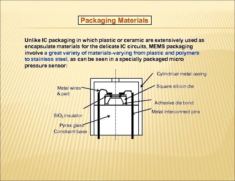 Packaging Materials Unlike IC packaging in which plastic or ceramic are extensively used as encapsulate materials for the delicate IC circuits, MEMS packaging involve a great variety of materials-varying from plastic and polymers to stainless steel, as can be seen in a specially packaged micro pressure sensor: Cylindrical metal casing Metal wires & pad Square silicon die Adhesive die bond Si. O 2 insulator Pyrex glass Constraint base Metal interconnect pins


