807ac1bad5fe38393b00971b0ecc723d.ppt
- Количество слайдов: 24
 Matching of Primitive Devices for Analog and Mixed Signal Applications “MOS-AK meeting, 21 Oct. 2002” Guenter Lau, Process Characterization, X-FAB Group
 Table of Contents l Matching - Mismatch, Reasons lead to Mismatch l Mismatch Variance Model, Hardware & Software Tools l MOS Transistor Matching l Resistor (& Contact) Matching l Bipolar Transistor Matching l Capacitor Matching l Plans for the Future The Mixed Signal Foundry Experts.
 Mismatch - Matching Definition Differences between identically designed components for analog devices are commonly associated with terms “matching” or “mismatch”. Types of mismatching The mismatch can have stochastic and systematic reasons. The Mixed Signal Foundry Experts.
 Mismatch - Matching Stochastic mismatch The stochastic mismatch caused by time-independent random variations in physical quantities is generally treated to be normally distributed and described by its standard deviation (s). Systematic mismatch When the average (µ) of the observed distribution is not zero, the term systematic mismatch is used. The Mixed Signal Foundry Experts.
 Local Parameter Variations l random local variations in doping concentration l built-in charges, local mobility fluctuations l oxide granularity l grain boundary distribution, doping fluctuations in poly gate l random dimensional variations (oxide thickness, polysilicon thickness, effective line width) “white noise” mismatch-generating process stochastic mismatch The Mixed Signal Foundry Experts.
 Global Parameter Variations l equipment induced non-uniformity's spatial (non random) variation across the wafer (e. g. gate oxide thickness, polysilicon line-width) temperature gradients due to and /or etch- and deposition rate variations additional stochastic mismatch (distance D) systematic mismatch (mean µ 0). The Mixed Signal Foundry Experts.
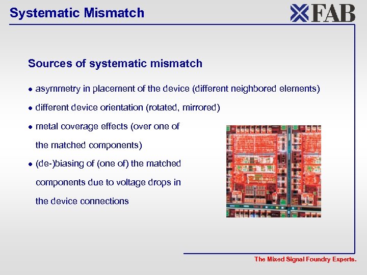 Systematic Mismatch Sources of systematic mismatch l asymmetry in placement of the device (different neighbored elements) l different device orientation (rotated, mirrored) l metal coverage effects (over one of the matched components) l (de-)biasing of (one of) the matched components due to voltage drops in the device connections The Mixed Signal Foundry Experts.
 Systematic Mismatch Sources of systematic mismatch l temperature differences due to non-uniform die heating (local dissipation) l stress non-uniformity's related to physical die (crystal) edges l stress non-uniformity's caused by packaging Measurements show that the systematic mismatch of “not carefully designed pairs” can reach considerable values and multiple exceed the stochastic mismatch. The Mixed Signal Foundry Experts.
 “Mismatch” caused by measurement system • Measurements performed quite near the resolution of the measurement system. The limited reproducibility and accuracy of the test system and asymmetry with respect to the probe card can influence the matching results stochastic and / or systematic mismatch. • Not the absolute accuracy of the parameters but there differences are important The Mixed Signal Foundry Experts.
 “Mismatch” caused by measurement system • To improve the measurement capability cmk, multiple measurements (5 - 20 times) were performed. The standard deviation of multiple measurements of one parameter (P) range from 0. 01 to 0. 04% ( to 0. 4 % for extrapolated parameters. ) The Mixed Signal Foundry Experts.
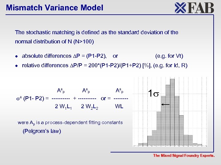 Mismatch Variance Model The stochastic matching is defined as the standard deviation of the normal distribution of N (N>100) l absolute differences P = (P 1 -P 2), l relative differences P/P = 200*(P 1 -P 2)/(P 1+P 2) [%], (e. g. for Id, R) or A²p A²p ² (P 1 - P 2) = ----- + ----- or = -------2 W 1 L 1 2 W 2 L 2 WL (e. g. for Vt) 1 were Ap is a process-dependent fitting constants (Pelgrom’s law) The Mixed Signal Foundry Experts.
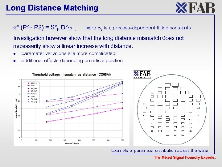 Long Distance Matching ² (P 1 - P 2) = S²p D² 12 , were Sp is a process-dependent fitting constants Investigation however show that the long distance mismatch does not necessarily show a linear increase with distance. l l parameter variations are more complicated. additional effects depending on reticle position Example of parameter distribution across the wafer The Mixed Signal Foundry Experts.
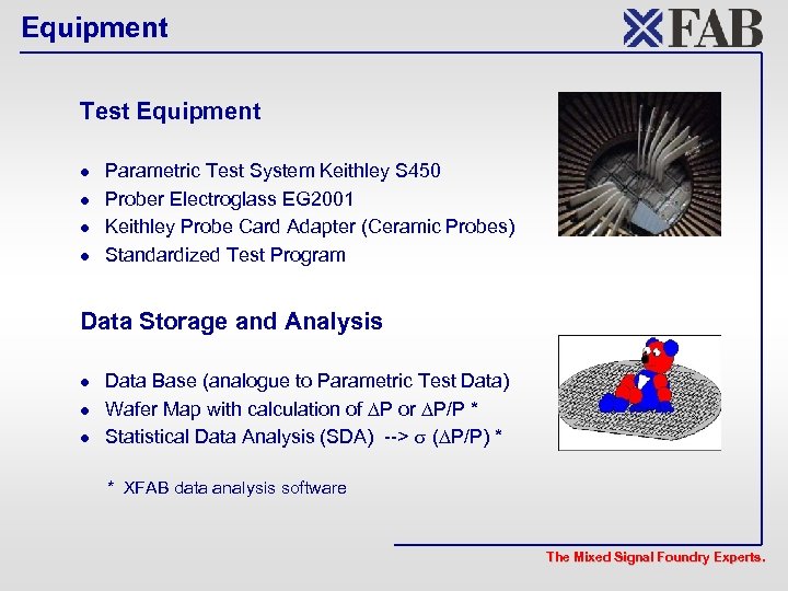 Equipment Test Equipment l l Parametric Test System Keithley S 450 Prober Electroglass EG 2001 Keithley Probe Card Adapter (Ceramic Probes) Standardized Test Program Data Storage and Analysis l l l Data Base (analogue to Parametric Test Data) Wafer Map with calculation of P or P/P * Statistical Data Analysis (SDA) --> ( P/P) * * XFAB data analysis software The Mixed Signal Foundry Experts.
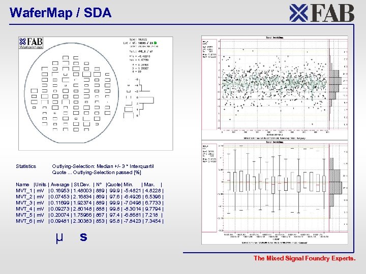 Wafer. Map / SDA Statistics Outlying-Selection: Median +/- 3 * Interquartil Quote. . . Outlying-Selection passed [%] Name |Units | Average | St. Dev. | N° |Quote| Min. | Max. | MVT_1 | m. V | 0. 16953 | 1. 48003 | 889 | 99. 9 | -5. 4821 | 4. 8228 | MVT_2 | m. V | 0. 07453 | 2. 16834 | 869 | 97. 6 | -6. 4926 | 6. 5396 | MVT_3 | m. V | 0. 11699 | 1. 92374 | 889 | 99. 9 | -7. 0498 | 6. 7733 | MVT_4 | m. V | 0. 09273 | 2. 80148 | 888 | 99. 8 | -8. 3014 | 9. 7794 | MVT_5 | m. V | 0. 20074 | 1. 75966 | 867 | 97. 4 | -6. 8681 | 7. 218 | MVT_6 | m. V | 0. 09481 | 2. 30383 | 853 | 95. 8 | -7. 8423 | 7. 3454 | µ s The Mixed Signal Foundry Experts.
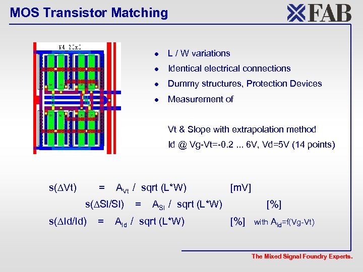 MOS Transistor Matching l L / W variations l Identical electrical connections l Dummy structures, Protection Devices l Measurement of Vt & Slope with extrapolation method Id @ Vg-Vt=-0. 2. . . 6 V, Vd=5 V (14 points) s( Vt) = AVt / sqrt (L*W) s( Sl/Sl) s( Id/Id) = = [m. V] ASl / sqrt (L*W) AId / sqrt (L*W) [%] with AId=f(Vg-Vt) The Mixed Signal Foundry Experts.
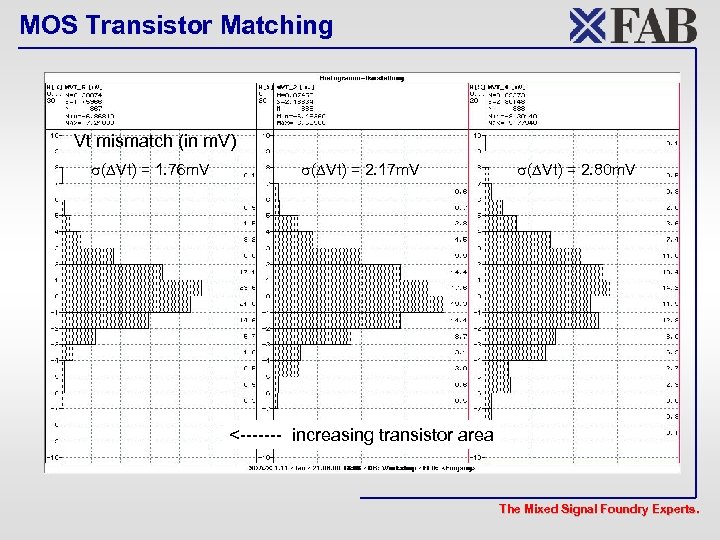 MOS Transistor Matching Vt mismatch (in m. V) ( Vt) = 1. 76 m. V ( Vt) = 2. 17 m. V ( Vt) = 2. 80 m. V <------- increasing transistor area The Mixed Signal Foundry Experts.
![( Vt) [m. V] MOS Transistor Matching 1 / sqrt (L*W) [1/µm] The ( Vt) [m. V] MOS Transistor Matching 1 / sqrt (L*W) [1/µm] The](https://present5.com/presentation/807ac1bad5fe38393b00971b0ecc723d/image-17.jpg) ( Vt) [m. V] MOS Transistor Matching 1 / sqrt (L*W) [1/µm] The Mixed Signal Foundry Experts.
( Vt) [m. V] MOS Transistor Matching 1 / sqrt (L*W) [1/µm] The Mixed Signal Foundry Experts.
![MOS Transistor Matching ( ID/ID) [%] 60% VG - VT [V] The Mixed Signal MOS Transistor Matching ( ID/ID) [%] 60% VG - VT [V] The Mixed Signal](https://present5.com/presentation/807ac1bad5fe38393b00971b0ecc723d/image-18.jpg) MOS Transistor Matching ( ID/ID) [%] 60% VG - VT [V] The Mixed Signal Foundry Experts.
MOS Transistor Matching ( ID/ID) [%] 60% VG - VT [V] The Mixed Signal Foundry Experts.
![( ID/ID) [%] MOS Transistor Matching 1 / sqrt (L*W) [1/µm] The Mixed ( ID/ID) [%] MOS Transistor Matching 1 / sqrt (L*W) [1/µm] The Mixed](https://present5.com/presentation/807ac1bad5fe38393b00971b0ecc723d/image-19.jpg) ( ID/ID) [%] MOS Transistor Matching 1 / sqrt (L*W) [1/µm] The Mixed Signal Foundry Experts.
( ID/ID) [%] MOS Transistor Matching 1 / sqrt (L*W) [1/µm] The Mixed Signal Foundry Experts.
![AID [%µm] MOS Transistor Matching VG - VT [V] The Mixed Signal Foundry Experts. AID [%µm] MOS Transistor Matching VG - VT [V] The Mixed Signal Foundry Experts.](https://present5.com/presentation/807ac1bad5fe38393b00971b0ecc723d/image-20.jpg) AID [%µm] MOS Transistor Matching VG - VT [V] The Mixed Signal Foundry Experts.
AID [%µm] MOS Transistor Matching VG - VT [V] The Mixed Signal Foundry Experts.
 MOS Transistor Matching l The Vt and the Slope mismatch calculations show some limitations (especially for large devices) due to the limited resolution of the extrapolated method new method necessary. l The direct measured drain currents give more reliable results. l The drain current mismatch not only depends on the transistor area but also strongly depends on the operating conditions. The Mixed Signal Foundry Experts.
 MOS Transistor Matching l Near the threshold voltage the Id mismatch drastically increases and shows an “saturation” in the sub-threshold region. l The mismatch behavior quit good follow the simple 1/sqrt(LW) law, only short and narrow (<= 0. 8 µm) transistors sometimes show an poorer matching when predicted (additional L and W effects). The Mixed Signal Foundry Experts.
 Matching Analysis - Basic Principle The deal with matching measurements and the following data analysis seems to be sometimes very mysterious and gives a lot of riddles. That’s why: Only the natural views made before the subtle comes, and always first of all try whether somewhat quite simply and naturally can be explained. G. Chr. Lichtenberg The Mixed Signal Foundry Experts.
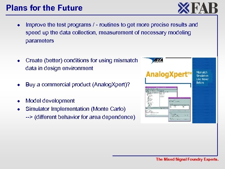 Plans for the Future l l l Improve the test programs / - routines to get more precise results and speed up the data collection, measurement of necessary modeling parameters Create (better) conditions for using mismatch data in design environment Buy a commercial product (Analog. Xpert)? Model development Simulator Implementation (Monte Carlo) --> (different behavior for area dependence) The Mixed Signal Foundry Experts.


