584940ae3236287c414f2941be04f246.ppt
- Количество слайдов: 94
Manufacturing Process [Adapted from Rabaey’s Digital Integrated Circuits, © 2002, J. Rabaey et al. and presentation by J. Christiansen/CERN] EE 415 VLSI Design
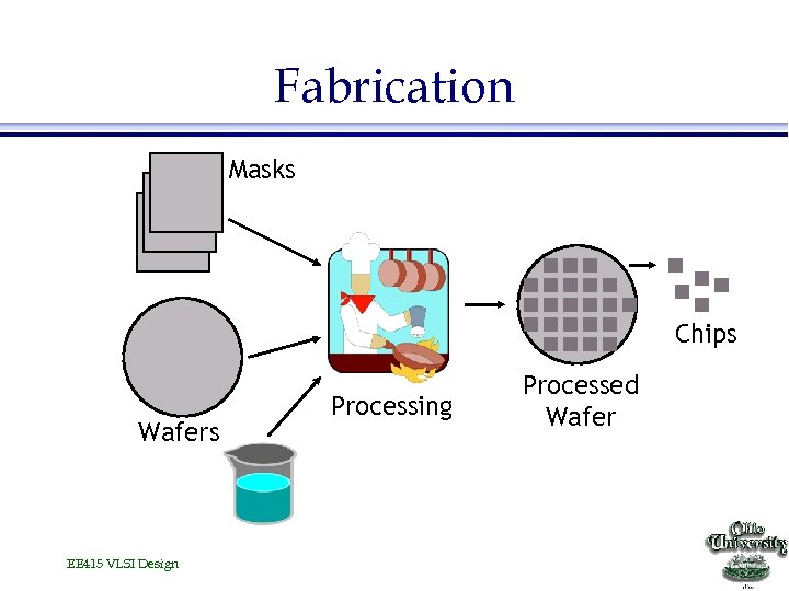
Fabrication Masks Chips Wafers EE 415 VLSI Design Processing Processed Wafer
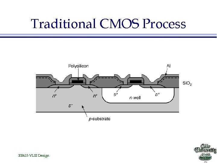
Traditional CMOS Process EE 415 VLSI Design
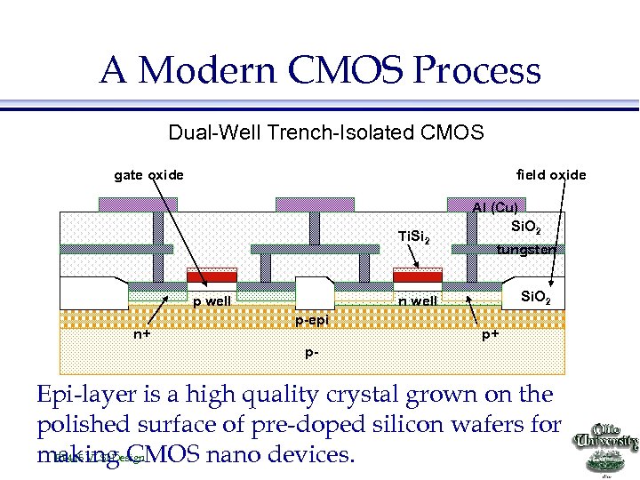
A Modern CMOS Process Dual-Well Trench-Isolated CMOS gate oxide field oxide Ti. Si 2 p well n+ Al (Cu) Si. O 2 tungsten Si. O 2 n well p-epi p+ p- Epi-layer is a high quality crystal grown on the polished surface of pre-doped silicon wafers for EE 415 VLSI Design making CMOS nano devices.

Photo-Lithographic Process optical mask oxidation photoresist removal (ashing) photoresist coating stepper exposure Typical operations in a single photolithographic cycle (from [Fullman]). photoresist development acid etch process step EE 415 VLSI Design spin, rinse, dry
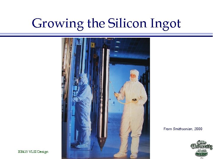
Growing the Silicon Ingot From Smithsonian, 2000 EE 415 VLSI Design
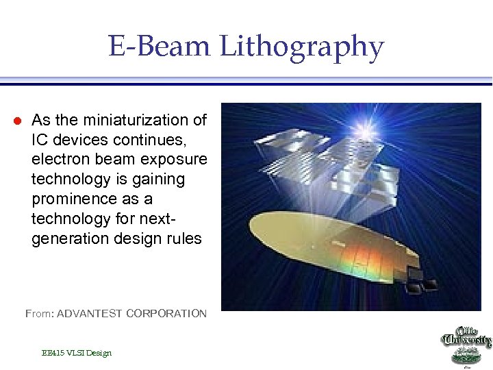
E-Beam Lithography l As the miniaturization of IC devices continues, electron beam exposure technology is gaining prominence as a technology for nextgeneration design rules From: ADVANTEST CORPORATION EE 415 VLSI Design
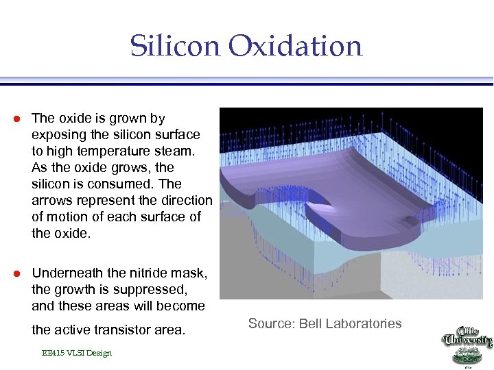
Silicon Oxidation l The oxide is grown by exposing the silicon surface to high temperature steam. As the oxide grows, the silicon is consumed. The arrows represent the direction of motion of each surface of the oxide. l Underneath the nitride mask, the growth is suppressed, and these areas will become the active transistor area. EE 415 VLSI Design Source: Bell Laboratories
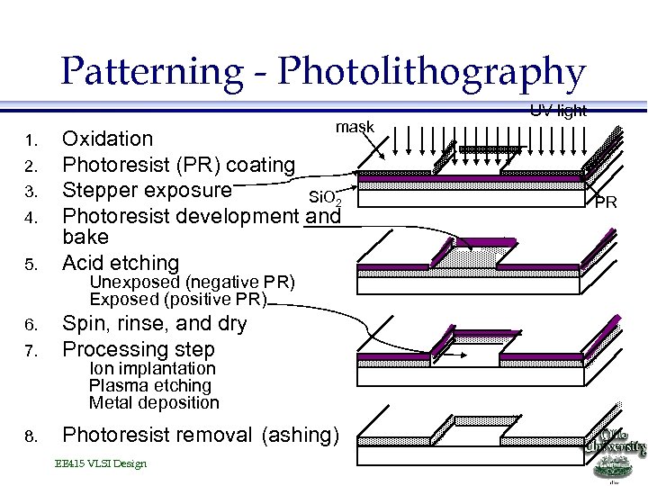
Patterning - Photolithography 1. 2. 3. 4. 5. mask Oxidation Photoresist (PR) coating Stepper exposure Si. O 2 Photoresist development and bake Acid etching Unexposed (negative PR) Exposed (positive PR) 7. Spin, rinse, and dry Processing step 8. Photoresist removal (ashing) 6. Ion implantation Plasma etching Metal deposition EE 415 VLSI Design UV light PR
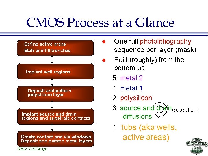
CMOS Process at a Glance Implant source and drain regions and substrate contacts One full photolithography sequence per layer (mask) Built (roughly) from the bottom up 5 metal 2 4 metal 1 2 polysilicon 3 source and drain exception! diffusions Create contact and via windows Deposit and pattern metal layers 1 tubs (aka wells, active areas) Define active areas Etch and fill trenches l l Implant well regions Deposit and pattern polysilicon layer EE 415 VLSI Design
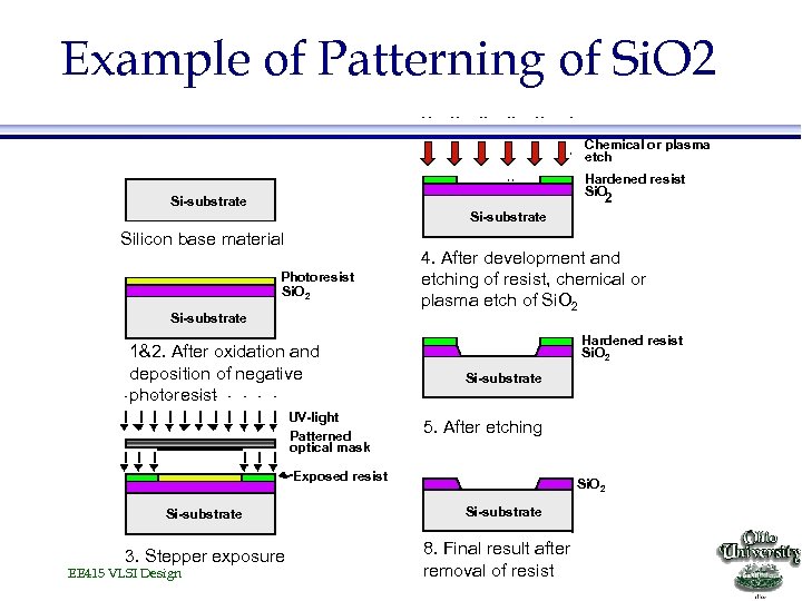
Example of Patterning of Si. O 2 Chemical or plasma etch Hardened resist Si. O 2 Si-substrate Silicon base material Photoresist Si. O 2 Si-substrate 1&2. After oxidation and deposition of negative photoresist UV-light Patterned optical mask 4. After development and etching of resist, chemical or plasma etch of Si. O 2 Hardened resist Si. O 2 Si-substrate 5. After etching Exposed resist Si-substrate 3. Stepper exposure EE 415 VLSI Design Si. O 2 Si-substrate 8. Final result after removal of resist
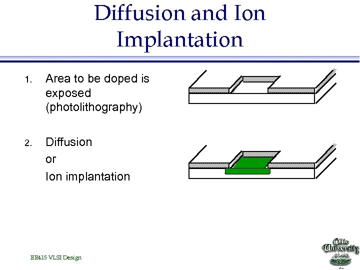
Diffusion and Ion Implantation 1. Area to be doped is exposed (photolithography) 2. Diffusion or Ion implantation EE 415 VLSI Design
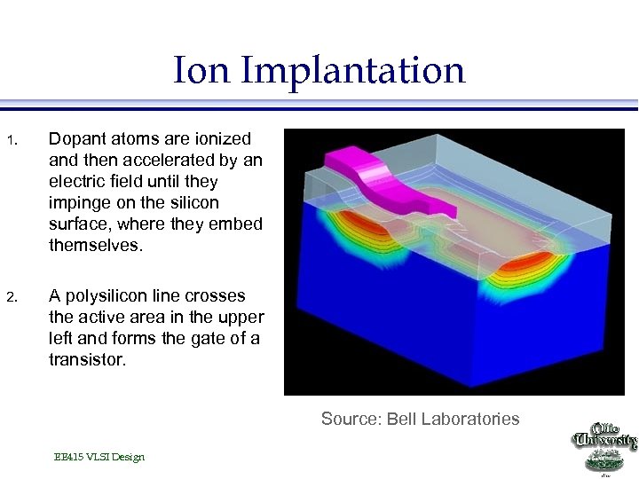
Ion Implantation 1. Dopant atoms are ionized and then accelerated by an electric field until they impinge on the silicon surface, where they embed themselves. 2. A polysilicon line crosses the active area in the upper left and forms the gate of a transistor. Source: Bell Laboratories EE 415 VLSI Design
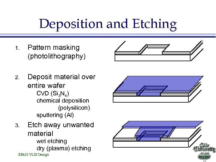
Deposition and Etching 1. Pattern masking (photolithography) 2. Deposit material over entire wafer CVD (Si 3 N 4) chemical deposition (polysilicon) sputtering (Al) 3. Etch away unwanted material wet etching dry (plasma) etching EE 415 VLSI Design
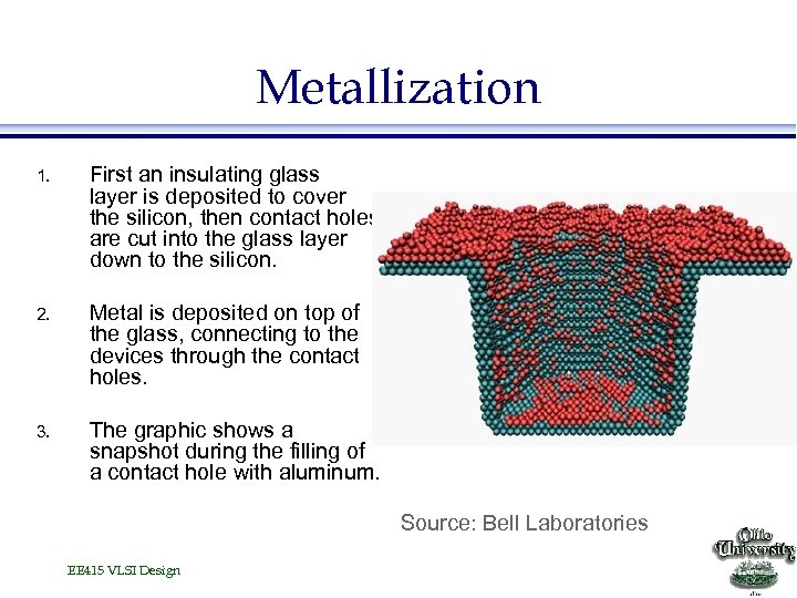
Metallization 1. First an insulating glass layer is deposited to cover the silicon, then contact holes are cut into the glass layer down to the silicon. 2. Metal is deposited on top of the glass, connecting to the devices through the contact holes. 3. The graphic shows a snapshot during the filling of a contact hole with aluminum. Source: Bell Laboratories EE 415 VLSI Design
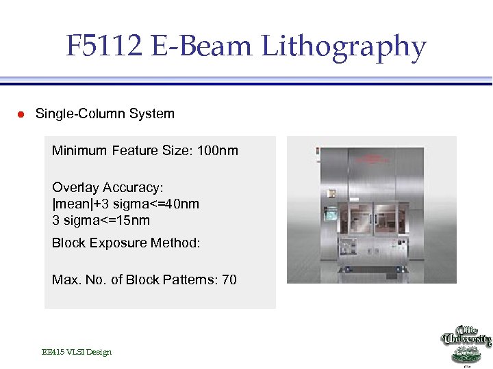
F 5112 E-Beam Lithography l Single-Column System Minimum Feature Size: 100 nm Overlay Accuracy: |mean|+3 sigma<=40 nm 3 sigma<=15 nm Block Exposure Method: Max. No. of Block Patterns: 70 EE 415 VLSI Design
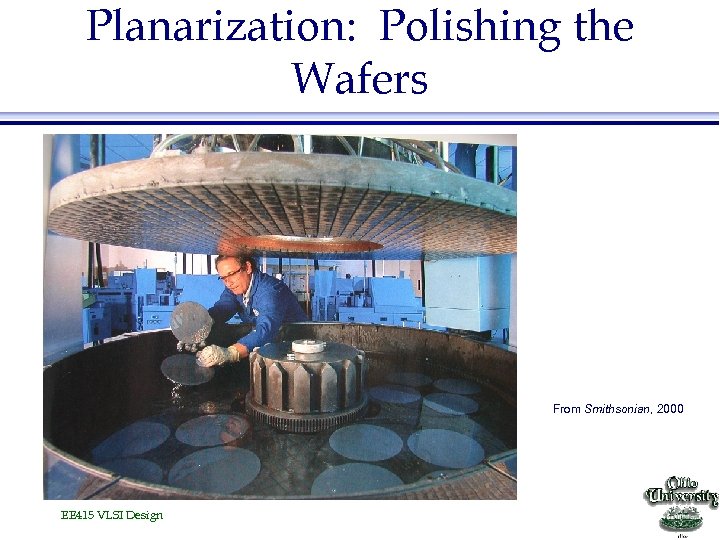
Planarization: Polishing the Wafers From Smithsonian, 2000 EE 415 VLSI Design
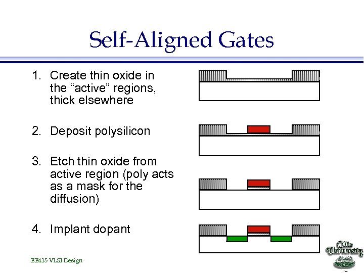
Self-Aligned Gates 1. Create thin oxide in the “active” regions, thick elsewhere 2. Deposit polysilicon 3. Etch thin oxide from active region (poly acts as a mask for the diffusion) 4. Implant dopant EE 415 VLSI Design
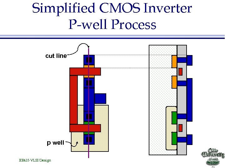
Simplified CMOS Inverter P-well Process cut line p well EE 415 VLSI Design
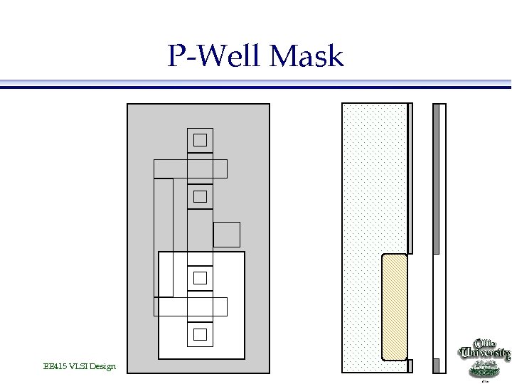
P-Well Mask EE 415 VLSI Design
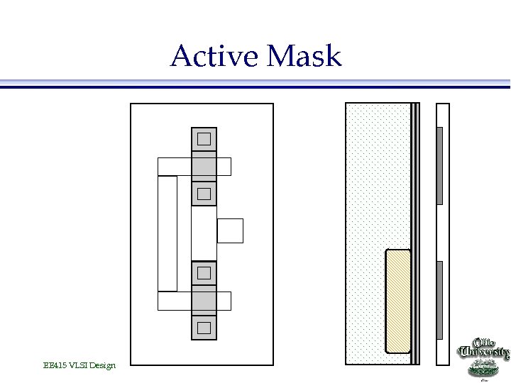
Active Mask EE 415 VLSI Design
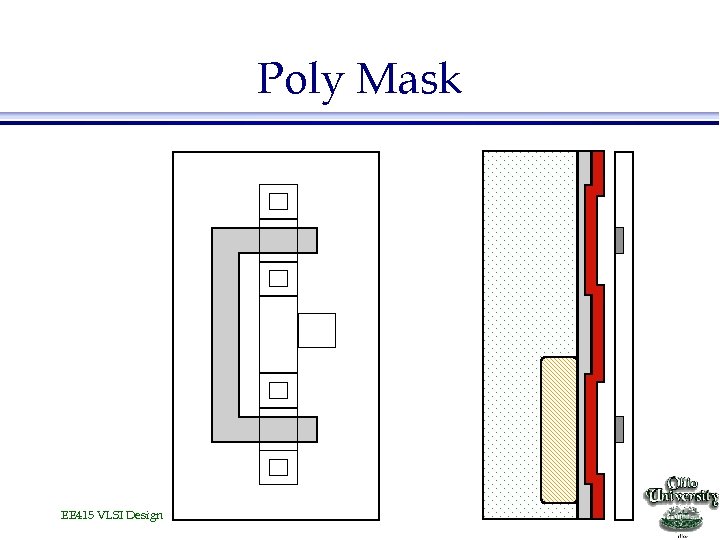
Poly Mask EE 415 VLSI Design
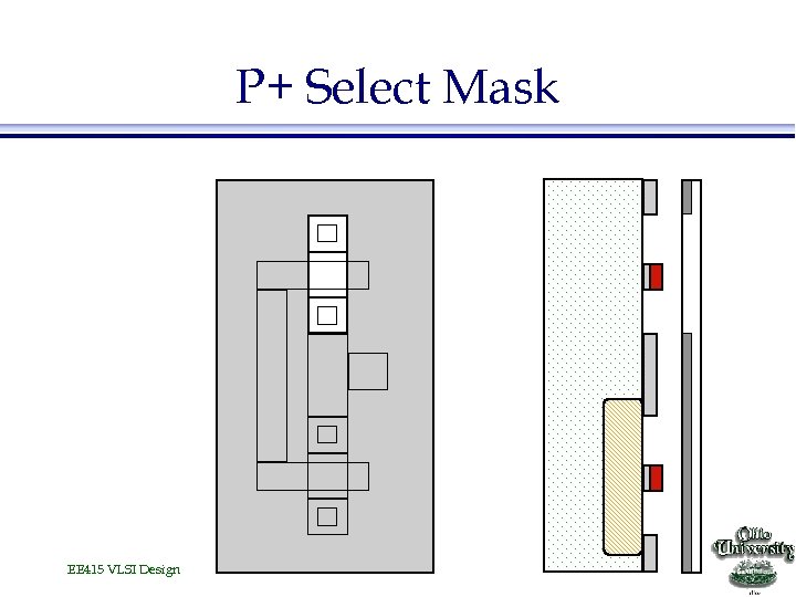
P+ Select Mask EE 415 VLSI Design
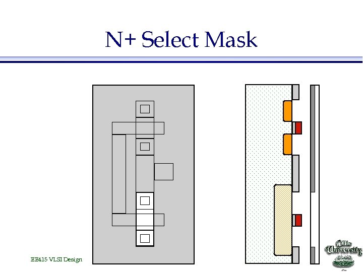
N+ Select Mask EE 415 VLSI Design
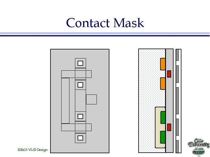
Contact Mask EE 415 VLSI Design
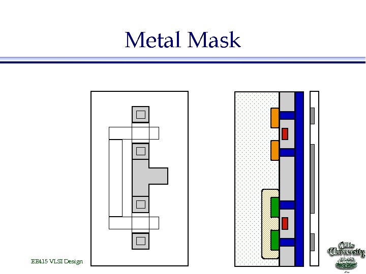
Metal Mask EE 415 VLSI Design
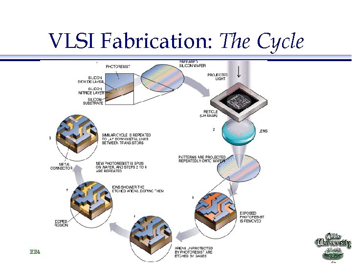
VLSI Fabrication: The Cycle EE 415 VLSI Design
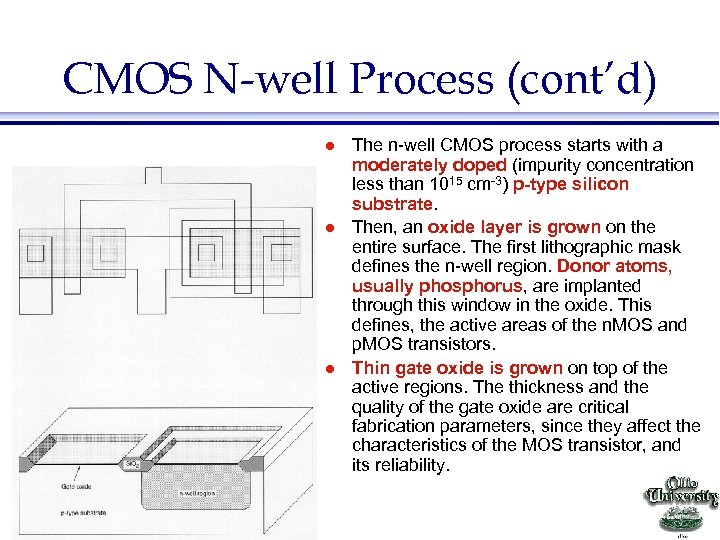
CMOS N-well Process (cont’d) l l l EE 415 VLSI Design The n-well CMOS process starts with a moderately doped (impurity concentration less than 1015 cm-3) p-type silicon substrate. Then, an oxide layer is grown on the entire surface. The first lithographic mask defines the n-well region. Donor atoms, usually phosphorus, are implanted through this window in the oxide. This defines, the active areas of the n. MOS and p. MOS transistors. Thin gate oxide is grown on top of the active regions. The thickness and the quality of the gate oxide are critical fabrication parameters, since they affect the characteristics of the MOS transistor, and its reliability.
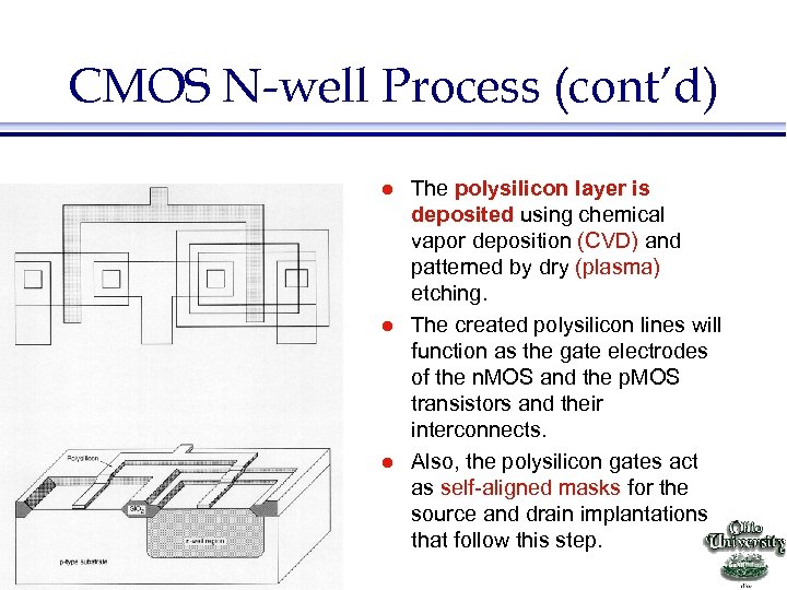
CMOS N-well Process (cont’d) l l l EE 415 VLSI Design The polysilicon layer is deposited using chemical vapor deposition (CVD) and patterned by dry (plasma) etching. The created polysilicon lines will function as the gate electrodes of the n. MOS and the p. MOS transistors and their interconnects. Also, the polysilicon gates act as self-aligned masks for the source and drain implantations that follow this step.
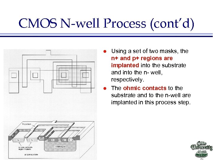
CMOS N-well Process (cont’d) l l EE 415 VLSI Design Using a set of two masks, the n+ and p+ regions are implanted into the substrate and into the n- well, respectively. The ohmic contacts to the substrate and to the n-well are implanted in this process step.
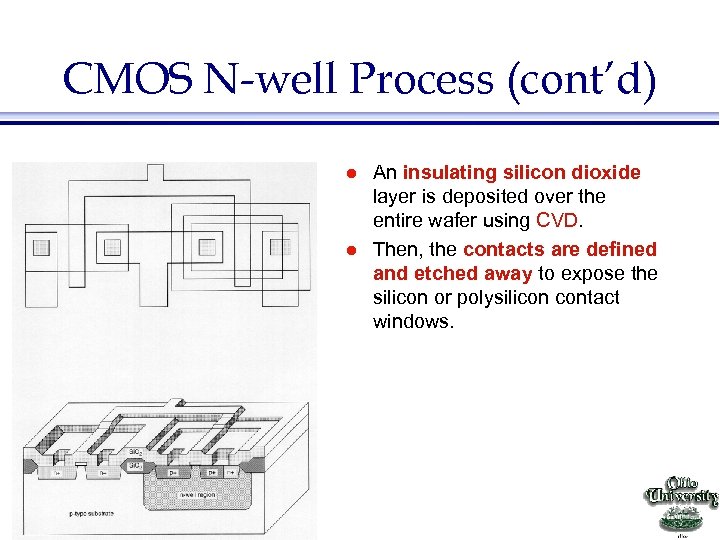
CMOS N-well Process (cont’d) l l EE 415 VLSI Design An insulating silicon dioxide layer is deposited over the entire wafer using CVD. Then, the contacts are defined and etched away to expose the silicon or polysilicon contact windows.
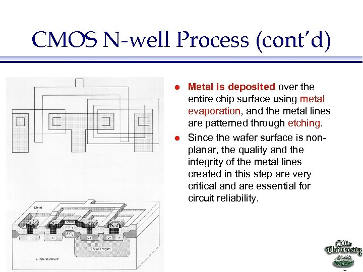
CMOS N-well Process (cont’d) l l EE 415 VLSI Design Metal is deposited over the entire chip surface using metal evaporation, and the metal lines are patterned through etching. Since the wafer surface is nonplanar, the quality and the integrity of the metal lines created in this step are very critical and are essential for circuit reliability.
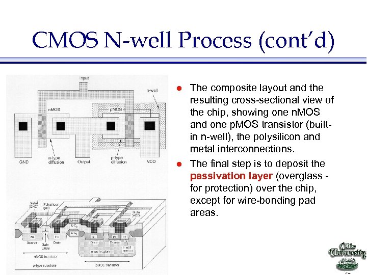
CMOS N-well Process (cont’d) l l EE 415 VLSI Design The composite layout and the resulting cross-sectional view of the chip, showing one n. MOS and one p. MOS transistor (builtin n-well), the polysilicon and metal interconnections. The final step is to deposit the passivation layer (overglass for protection) over the chip, except for wire-bonding pad areas.
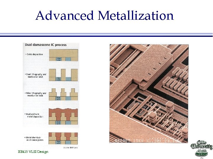
Advanced Metallization EE 415 VLSI Design
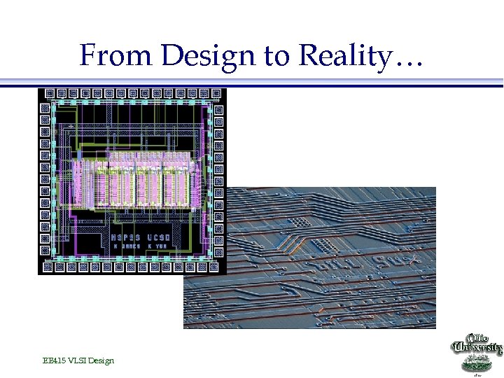
From Design to Reality… EE 415 VLSI Design

Design Rules EE 415 VLSI Design
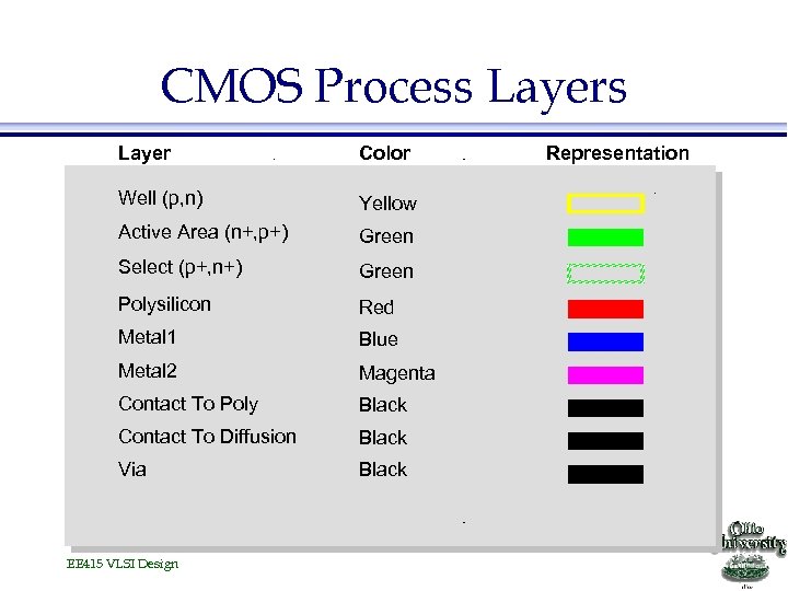
CMOS Process Layer Color Well (p, n) Yellow Active Area (n+, p+) Green Select (p+, n+) Green Polysilicon Red Metal 1 Blue Metal 2 Magenta Contact To Poly Black Contact To Diffusion Black Via Black EE 415 VLSI Design Representation
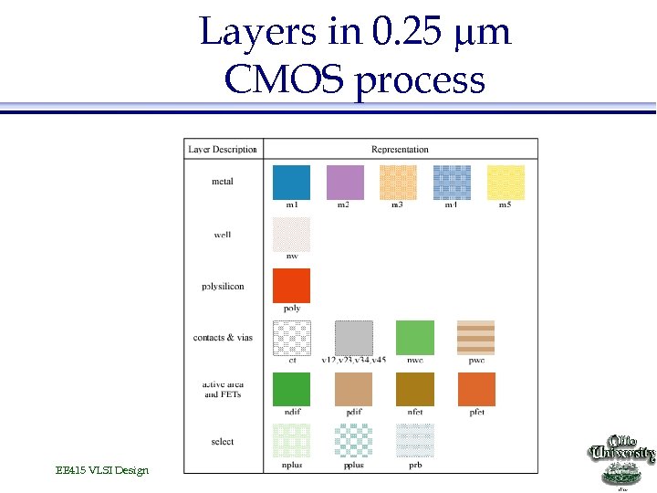
Layers in 0. 25 mm CMOS process EE 415 VLSI Design
Design Rules l l l Interface between the circuit designer and process engineer Guidelines for constructing process masks Unit dimension: minimum line width » scalable design rules: lambda parameter » absolute dimensions: micron rules l l Rules constructed to ensure that design works even when small fab errors (within some tolerance) occur A complete set includes » set of layers » intra-layer: relations between objects in the same layer » inter-layer: relations between objects on different layers EE 415 VLSI Design
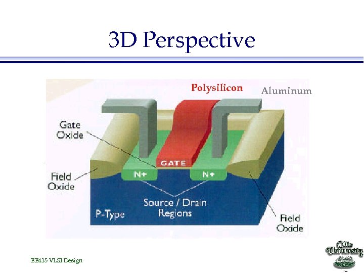
3 D Perspective Polysilicon EE 415 VLSI Design Aluminum
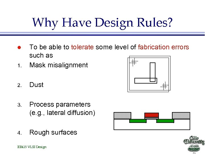
Why Have Design Rules? 1. To be able to tolerate some level of fabrication errors such as Mask misalignment 2. Dust 3. Process parameters (e. g. , lateral diffusion) 4. Rough surfaces l EE 415 VLSI Design
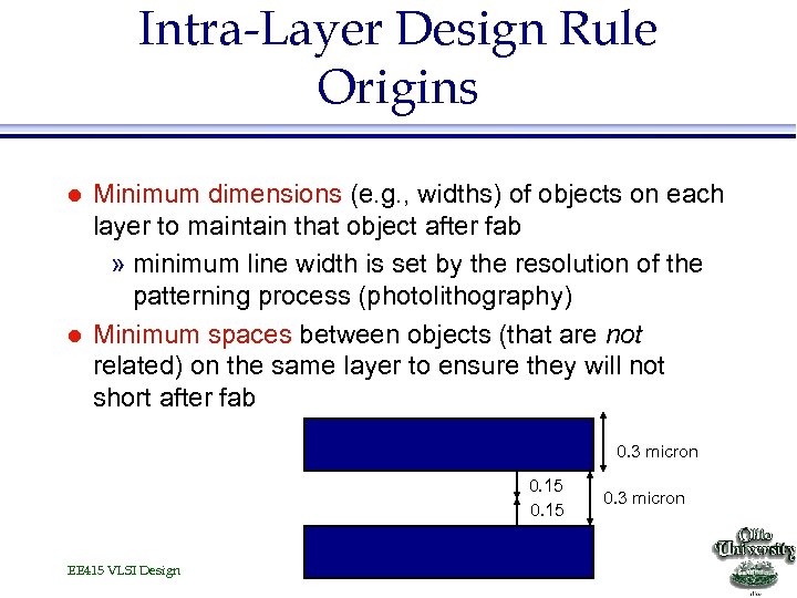
Intra-Layer Design Rule Origins l l Minimum dimensions (e. g. , widths) of objects on each layer to maintain that object after fab » minimum line width is set by the resolution of the patterning process (photolithography) Minimum spaces between objects (that are not related) on the same layer to ensure they will not short after fab 0. 3 micron 0. 15 EE 415 VLSI Design 0. 3 micron
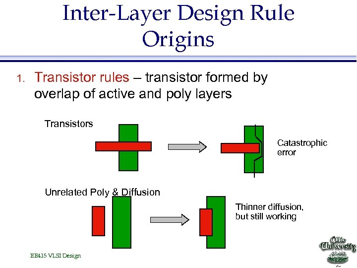
Inter-Layer Design Rule Origins 1. Transistor rules – transistor formed by overlap of active and poly layers Transistors Catastrophic error Unrelated Poly & Diffusion Thinner diffusion, but still working EE 415 VLSI Design
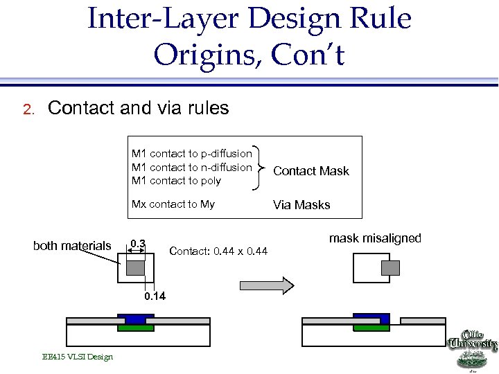
Inter-Layer Design Rule Origins, Con’t 2. Contact and via rules M 1 contact to p-diffusion M 1 contact to n-diffusion M 1 contact to poly Mx contact to My both materials Contact Mask Via Masks 0. 3 0. 14 EE 415 VLSI Design Contact: 0. 44 x 0. 44 mask misaligned
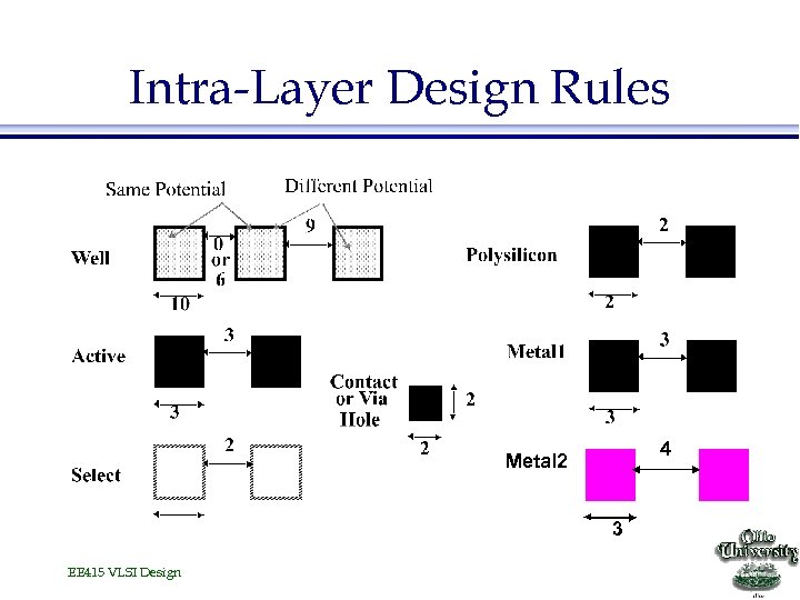
Intra-Layer Design Rules 4 Metal 2 3 EE 415 VLSI Design
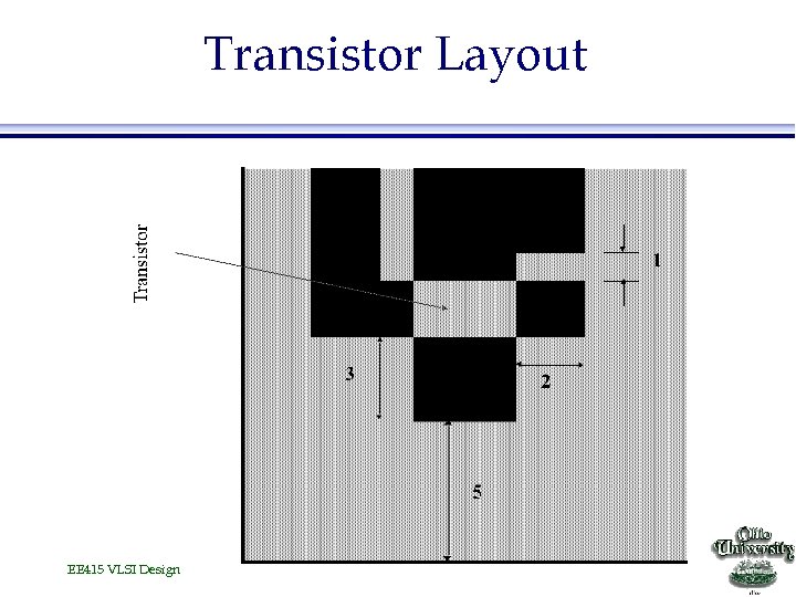
Transistor Layout EE 415 VLSI Design
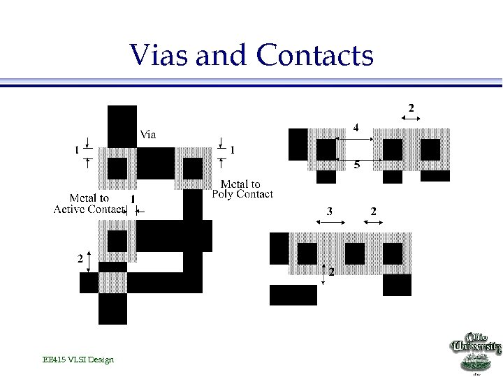
Vias and Contacts EE 415 VLSI Design
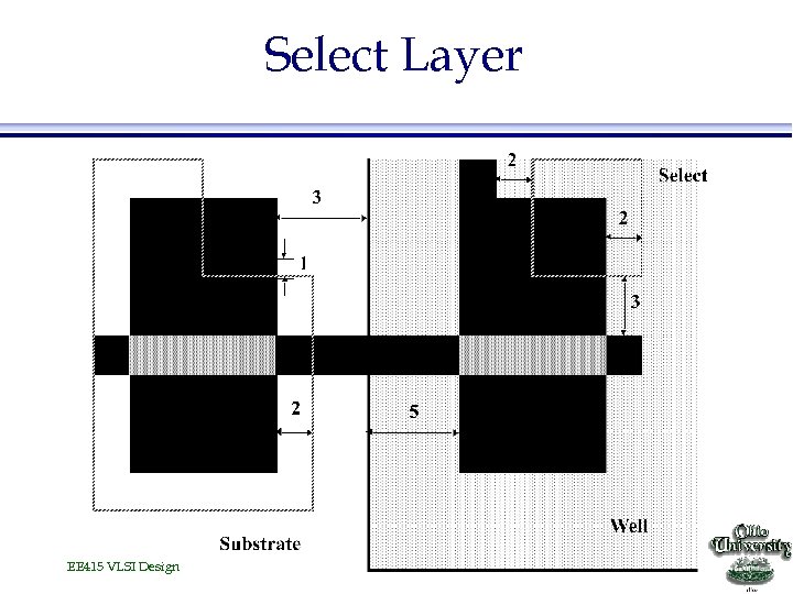
Select Layer EE 415 VLSI Design

IC Layout EE 415 VLSI Design
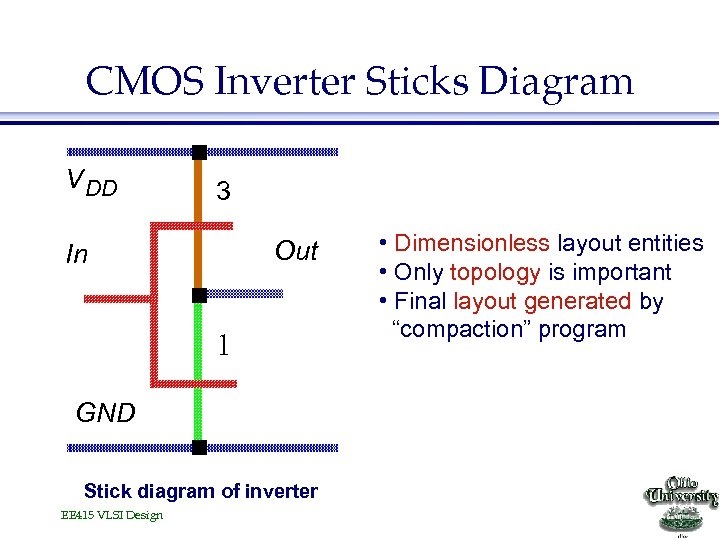
CMOS Inverter Sticks Diagram V DD 3 Out In 1 GND Stick diagram of inverter EE 415 VLSI Design • Dimensionless layout entities • Only topology is important • Final layout generated by “compaction” program
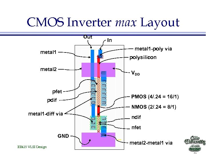
CMOS Inverter max Layout Out In metal 1 -poly via metal 1 polysilicon metal 2 VDD pfet pdif PMOS (4/. 24 = 16/1) NMOS (2/. 24 = 8/1) metal 1 -diff via ndif nfet GND EE 415 VLSI Design metal 2 -metal 1 via
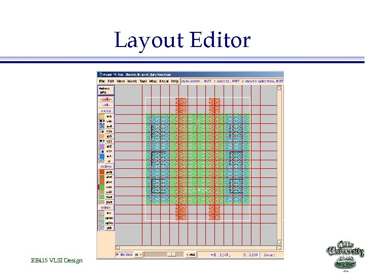
Layout Editor EE 415 VLSI Design
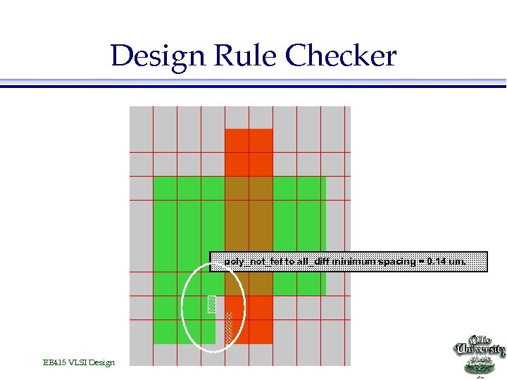
Design Rule Checker poly_not_fet to all_diff minimum spacing = 0. 14 um. EE 415 VLSI Design
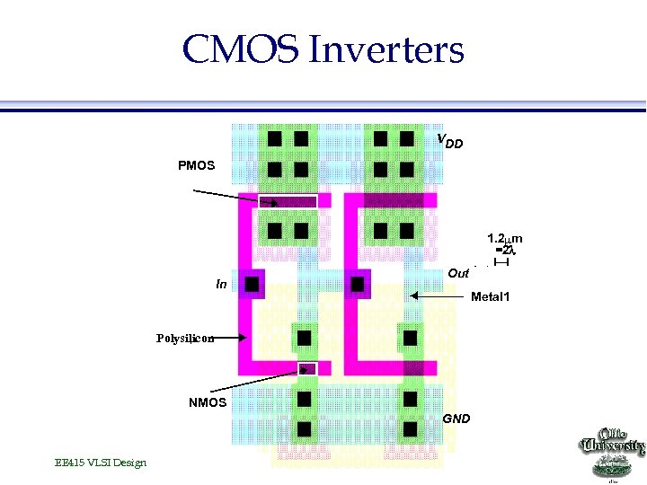
CMOS Inverters VDD PMOS 1. 2 mm =2 l In Out Metal 1 Polysilicon NMOS GND EE 415 VLSI Design
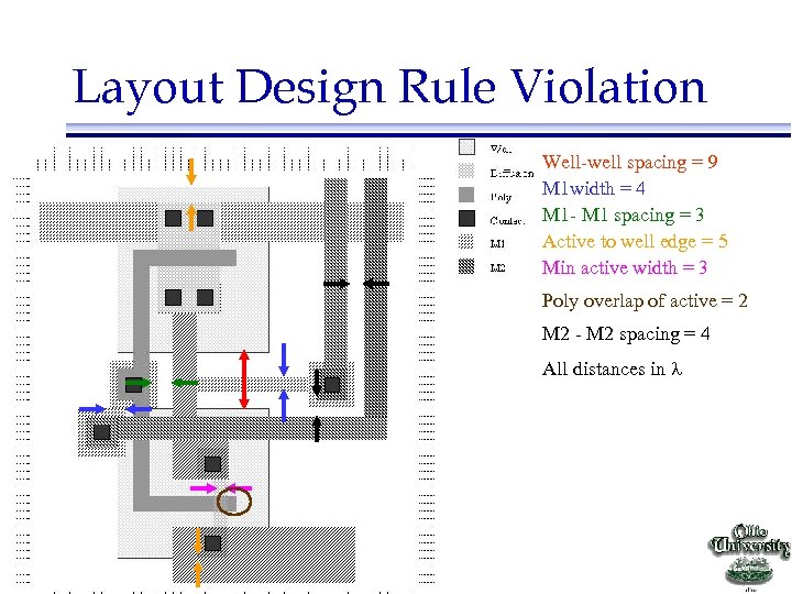
Layout Design Rule Violation Well-well spacing = 9 M 1 width = 4 M 1 - M 1 spacing = 3 Active to well edge = 5 Min active width = 3 Poly overlap of active = 2 M 2 - M 2 spacing = 4 All distances in l EE 415 VLSI Design
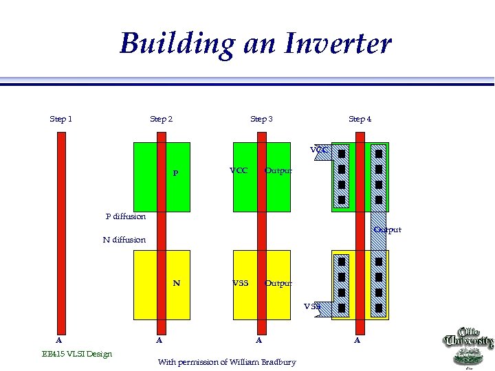
Building an Inverter Step 1 Step 2 Step 3 Step 4 VCC P VCC Output P diffusion Output N diffusion N VSS Output VSS A EE 415 VLSI Design A A With permission of William Bradbury A
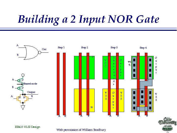
Building a 2 Input NOR Gate A Out Step 1 Step 2 B Step 3 P S h a r e d n o d e V C C A P Shared node B Step 4 O u t p u t VC C P Output A N N V S S B O u t p u t N A EE 415 VLSI Design B A B With permission of William Bradbury A V S S B V S S A B
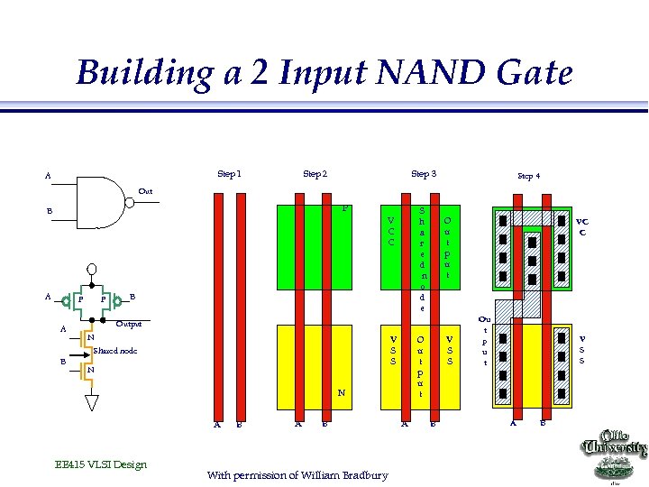
Building a 2 Input NAND Gate Step 1 A Step 2 Step 3 Step 4 Out P B S h a r e d n o d e V C C A P A B P B O u t p u t Output N Shared node V S S N O u t p u t N A EE 415 VLSI Design B A B With permission of William Bradbury A V S S B VC C Ou t p u t V S S A B
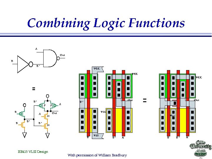
Combining Logic Functions A Out B B’ VCC VCC B’ P B B A B’ B’ A P N Out B’ VSS Out VSS N B EE 415 VLSI Design VSS B’ A With permission of William Bradbury B B’ A
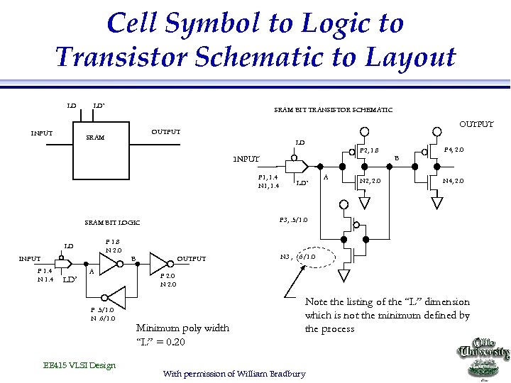
Cell Symbol to Logic to Transistor Schematic to Layout LD INPUT LD’ SRAM BIT TRANSISTOR SCHEMATIC OUTPUT SRAM LD P 2, 1. 8 INPUT P 1, 1. 4 N 1, 1. 4 P 1. 8 N 2. 0 INPUT P 1. 4 N 1. 4 LD’ A P. 5/1. 0 N. 6/1. 0 EE 415 VLSI Design A N 2, 2. 0 N 4, 2. 0 P 3, . 5/1. 0 SRAM BIT LOGIC LD LD’ P 4, 2. 0 B B OUTPUT N 3 , . 6/1. 0 P 2. 0 N 2. 0 Minimum poly width “L” = 0. 20 Note the listing of the “L” dimension which is not the minimum defined by the process With permission of William Bradbury
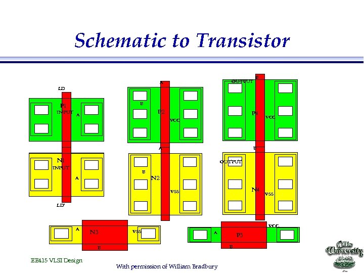
Schematic to Transistor OUTPUT A B LD B P 1 P 2 INPUT A P 4 VCC B A N 1 OUTPUT INPUT B A N 2 N 4 VSS LD’ A N 3 VSS VCC A B B EE 415 VLSI Design P 3 With permission of William Bradbury
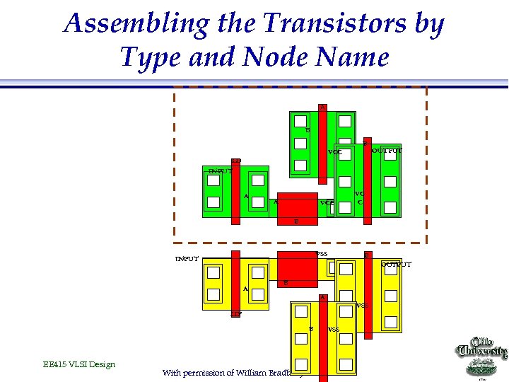
Assembling the Transistors by Type and Node Name A B B VCC OUTPUT LD INPUT A A VCC VC C B VSS INPUT B OUTPUT A B A VSS LD’ B EE 415 VLSI Design With permission of William Bradbury VSS
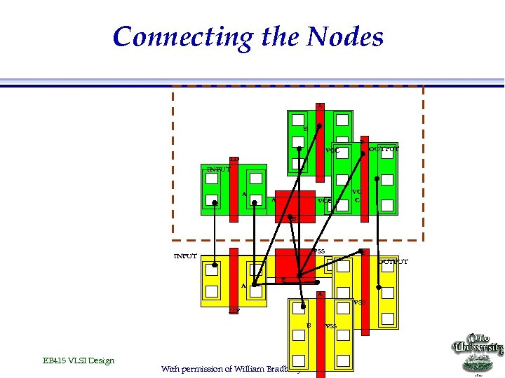
Connecting the Nodes A B B VCC OUTPUT LD INPUT A A VCC VC C B VSS INPUT B OUTPUT A B A VSS LD’ B EE 415 VLSI Design With permission of William Bradbury VSS
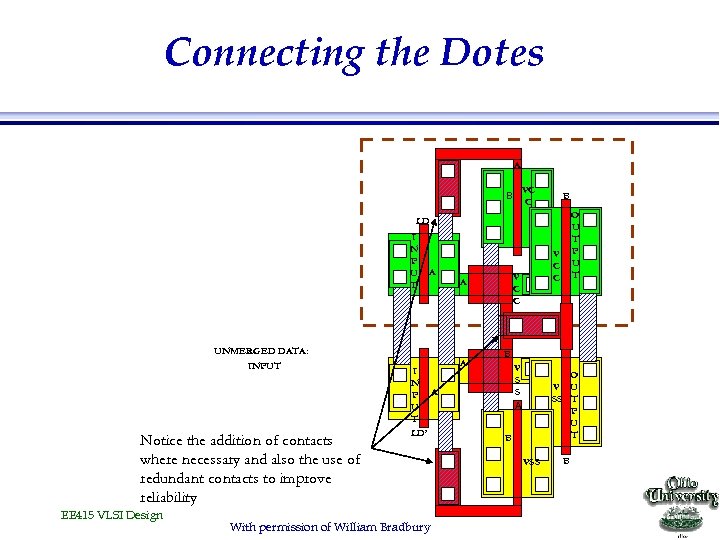
Connecting the Dotes A VC C B B O U T P U T LD I N P U T A V C C A B UNMERGED DATA: INPUT Notice the addition of contacts where necessary and also the use of redundant contacts to improve reliability EE 415 VLSI Design I N P A U T LD’ With permission of William Bradbury A V C C B V S S A O V U SS T P U T B VSS B
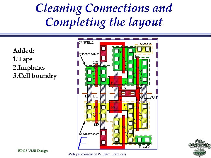
Cleaning Connections and Completing the layout. N-WELL Added: 1. Taps 2. Implants 3. Cell boundry B P-IMPLANT P 2 V C C LD DD P 1 IN P A U T A V P C 3 B B C INPUT N 1 IN PU A T LD’ N-IMPLANT EE 415 VLSI Design N-TAP A B N 3 VS S P 4 O VC U C T P U BT B B OUTPUT N 4 OU TP VS UT S B A N 2 VS S P-TAP With permission of William Bradbury
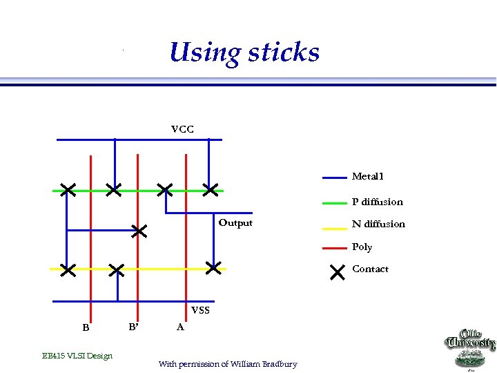
Using sticks . VCC Metal 1 P diffusion Output N diffusion Poly Contact VSS B EE 415 VLSI Design B’ A With permission of William Bradbury
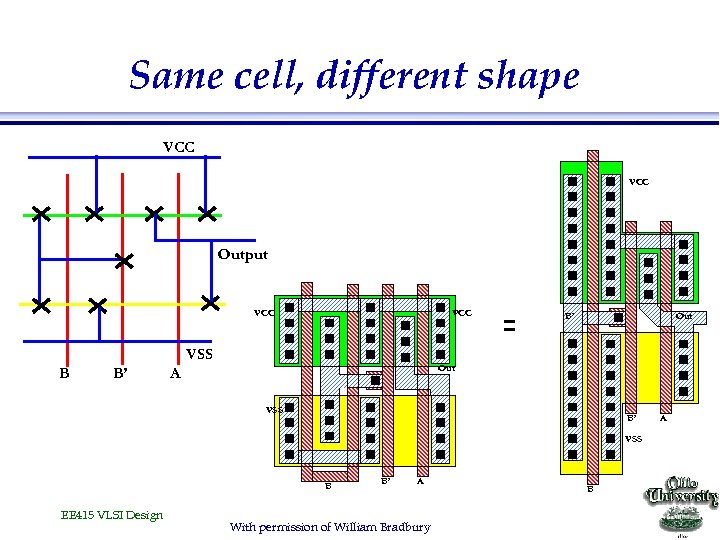
Same cell, different shape. VCC Output VCC VSS B B’ B’ Out A VSS B’ VSS B EE 415 VLSI Design B’ A With permission of William Bradbury B A
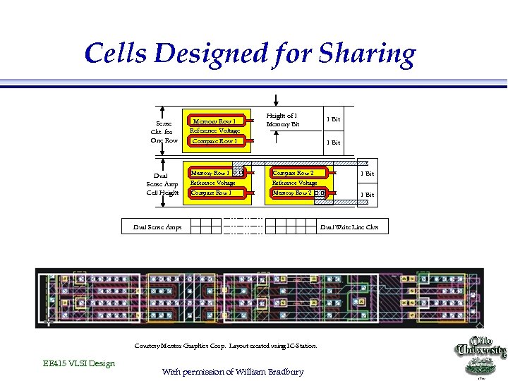
Cells Designed for Sharing. Sense Ckt. for One Row Dual Sense Amp Cell Height Memory Row 1 Reference Voltage Height of 1 Memory Bit Compare Row 1 1 Bit Memory Row 1 Compare Row 2 Reference Voltage Compare Row 1 Memory Row 2 Dual Sense Amps Courtesy Mentor Graphics Corp. Layout created using IC-Station. EE 415 VLSI Design 1 Bit With permission of William Bradbury 1 Bit Dual Write Line Ckts
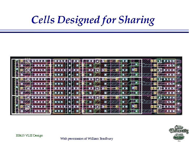
Cells Designed for Sharing. EE 415 VLSI Design With permission of William Bradbury
Packaging EE 415 VLSI Design
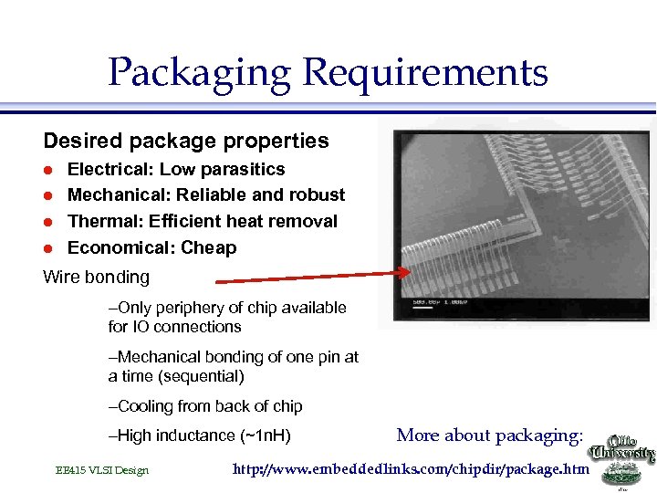
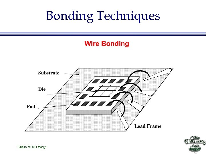
Packaging Requirements Desired package properties l l Electrical: Low parasitics Mechanical: Reliable and robust Thermal: Efficient heat removal Economical: Cheap Wire bonding –Only periphery of chip available for IO connections –Mechanical bonding of one pin at a time (sequential) –Cooling from back of chip –High inductance (~1 n. H) EE 415 VLSI Design More about packaging: http: //www. embeddedlinks. com/chipdir/package. htm
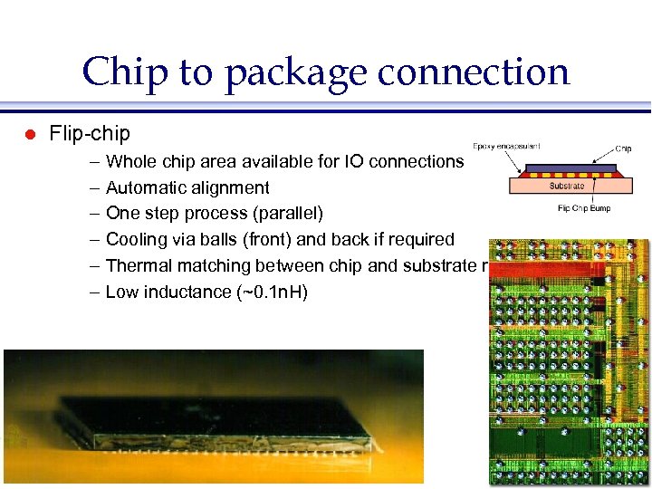
Chip to package connection l Flip-chip – – – Whole chip area available for IO connections Automatic alignment One step process (parallel) Cooling via balls (front) and back if required Thermal matching between chip and substrate required Low inductance (~0. 1 n. H) EE 415 VLSI Design
Bonding Techniques EE 415 VLSI Design
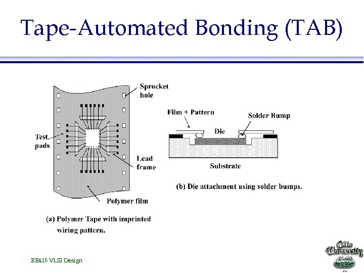
Tape-Automated Bonding (TAB) EE 415 VLSI Design
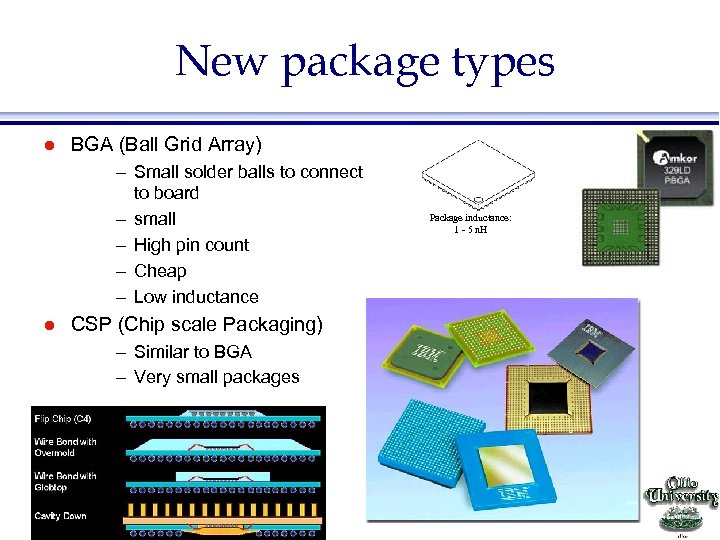
New package types l BGA (Ball Grid Array) – Small solder balls to connect to board – small – High pin count – Cheap – Low inductance l CSP (Chip scale Packaging) – Similar to BGA – Very small packages EE 415 VLSI Design Package inductance: 1 - 5 n. H
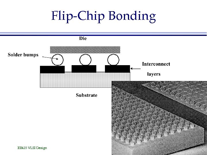
Flip-Chip Bonding EE 415 VLSI Design
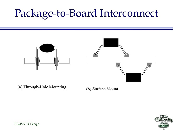
Package-to-Board Interconnect EE 415 VLSI Design
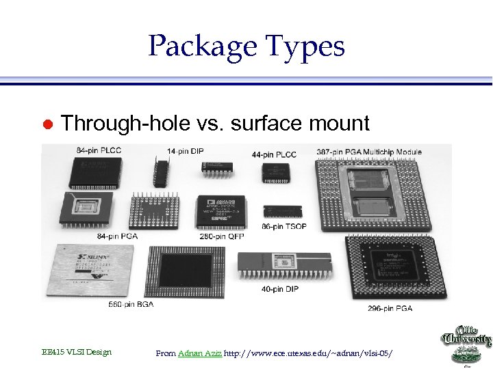
Package Types l Through-hole vs. surface mount EE 415 VLSI Design From Adnan Aziz http: //www. ece. utexas. edu/~adnan/vlsi-05/
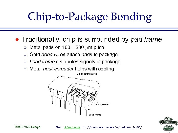
Chip-to-Package Bonding l Traditionally, chip is surrounded by pad frame » » Metal pads on 100 – 200 mm pitch Gold bond wires attach pads to package Lead frame distributes signals in package Metal heat spreader helps with cooling EE 415 VLSI Design From Adnan Aziz http: //www. ece. utexas. edu/~adnan/vlsi-05/
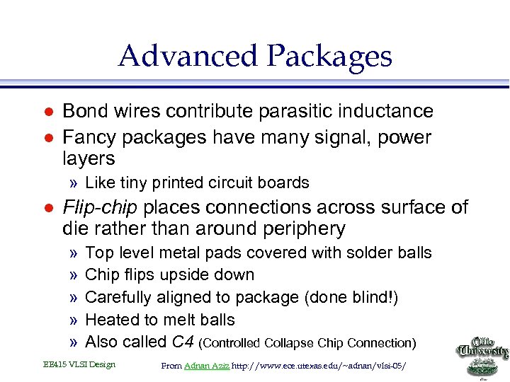
Advanced Packages l l Bond wires contribute parasitic inductance Fancy packages have many signal, power layers » Like tiny printed circuit boards l Flip-chip places connections across surface of die rather than around periphery » » » Top level metal pads covered with solder balls Chip flips upside down Carefully aligned to package (done blind!) Heated to melt balls Also called C 4 (Controlled Collapse Chip Connection) EE 415 VLSI Design From Adnan Aziz http: //www. ece. utexas. edu/~adnan/vlsi-05/
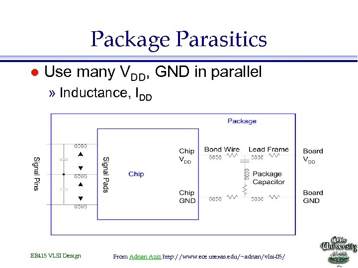
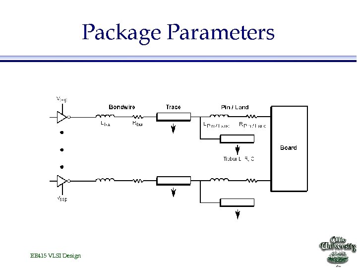
Package Parasitics l Use many VDD, GND in parallel » Inductance, IDD EE 415 VLSI Design From Adnan Aziz http: //www. ece. utexas. edu/~adnan/vlsi-05/
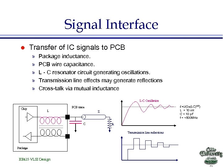
Signal Interface l Transfer of IC signals to PCB » » » Package inductance. PCB wire capacitance. L - C resonator circuit generating oscillations. Transmission line effects may generate reflections Cross-talk via mutual inductance L-C Oscillation Chip f =1/(2 p(LC)1/2) L = 10 n. H C = 10 p. F f = ~500 MHz PCB trace L Z C R Transmission line reflections Package EE 415 VLSI Design
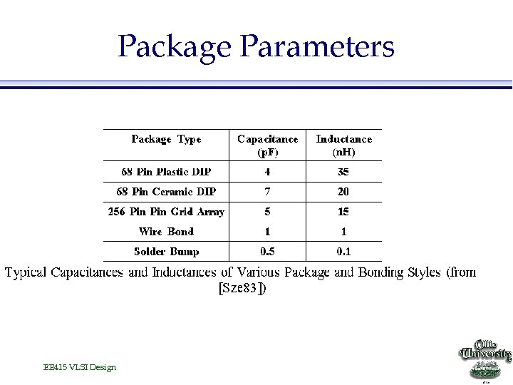
Package Parameters EE 415 VLSI Design
Package Parameters EE 415 VLSI Design
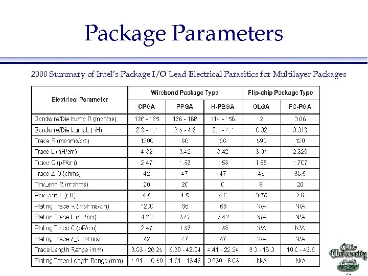
Package Parameters 2000 Summary of Intel’s Package I/O Lead Electrical Parasitics for Multilayer Packages EE 415 VLSI Design
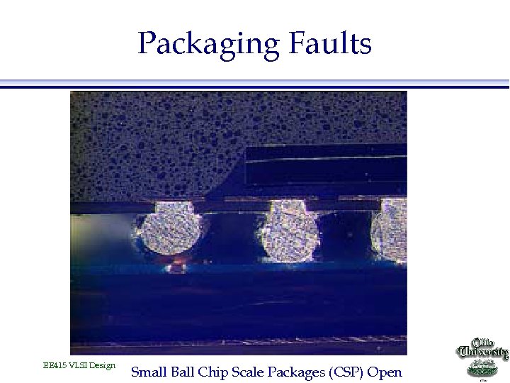
Packaging Faults EE 415 VLSI Design Small Ball Chip Scale Packages (CSP) Open
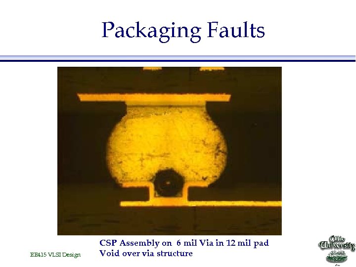
Packaging Faults EE 415 VLSI Design CSP Assembly on 6 mil Via in 12 mil pad Void over via structure
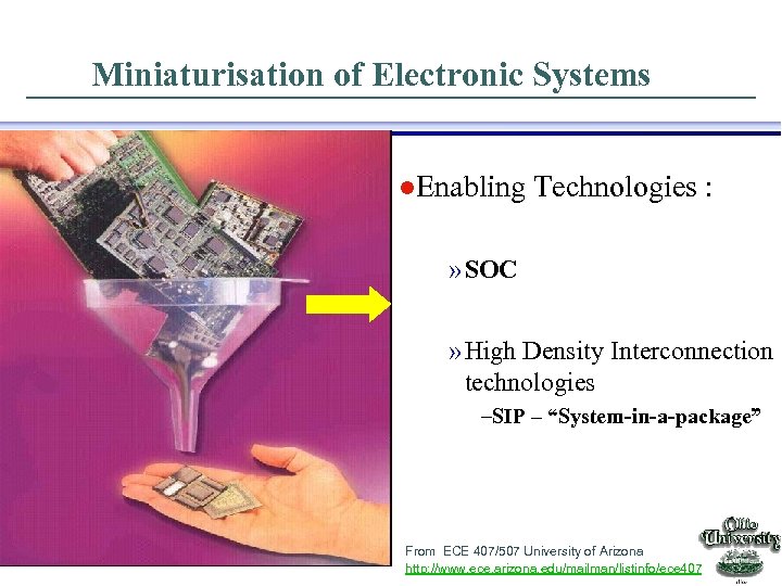
Miniaturisation of Electronic Systems l. Enabling Technologies : » SOC » High Density Interconnection technologies –SIP – “System-in-a-package” EE 415 VLSI Design From ECE 407/507 University of Arizona http: //www. ece. arizona. edu/mailman/listinfo/ece 407
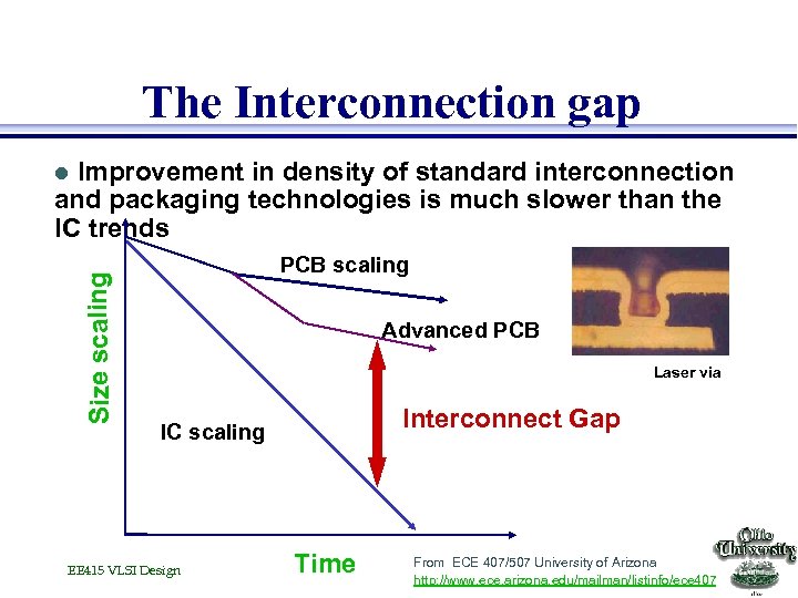
The Interconnection gap Improvement in density of standard interconnection and packaging technologies is much slower than the IC trends Size scaling l PCB scaling Advanced PCB Laser via Interconnect Gap IC scaling EE 415 VLSI Design Time From ECE 407/507 University of Arizona http: //www. ece. arizona. edu/mailman/listinfo/ece 407
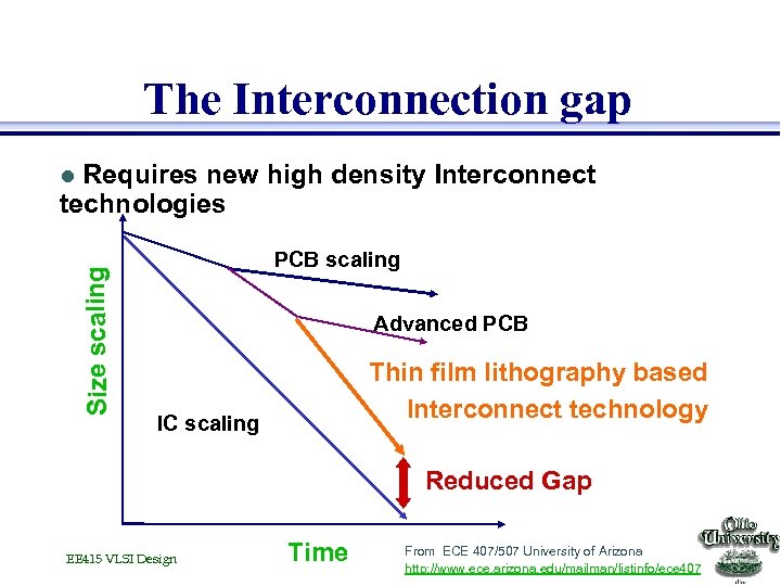
The Interconnection gap Requires new high density Interconnect technologies Size scaling l PCB scaling Advanced PCB Thin film lithography based Interconnect technology IC scaling Reduced Gap EE 415 VLSI Design Time From ECE 407/507 University of Arizona http: //www. ece. arizona. edu/mailman/listinfo/ece 407
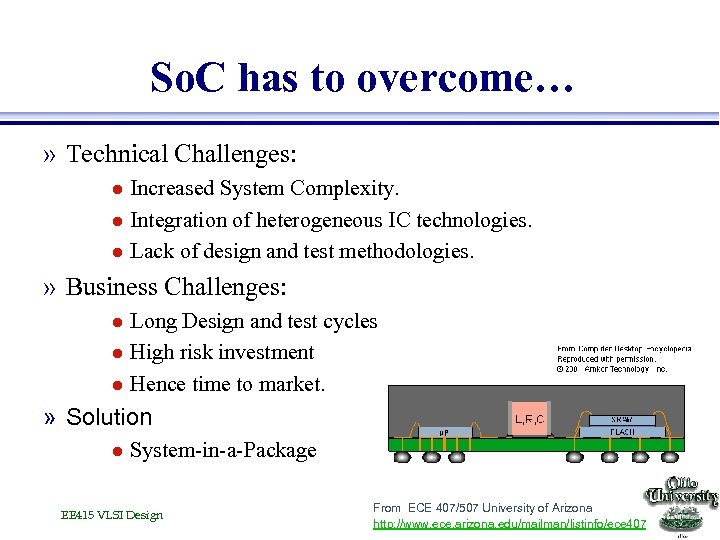
So. C has to overcome… » Technical Challenges: l l l Increased System Complexity. Integration of heterogeneous IC technologies. Lack of design and test methodologies. » Business Challenges: l l l Long Design and test cycles High risk investment Hence time to market. » Solution l System-in-a-Package EE 415 VLSI Design From ECE 407/507 University of Arizona http: //www. ece. arizona. edu/mailman/listinfo/ece 407
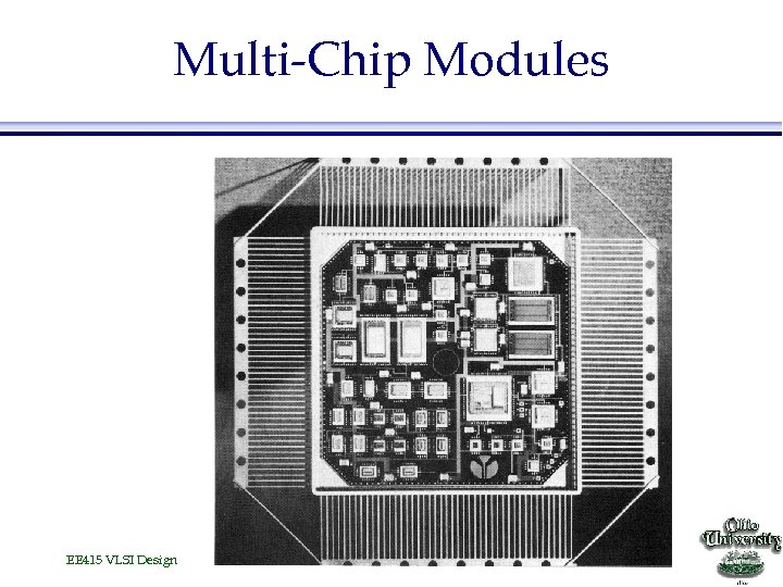
Multi-Chip Modules EE 415 VLSI Design
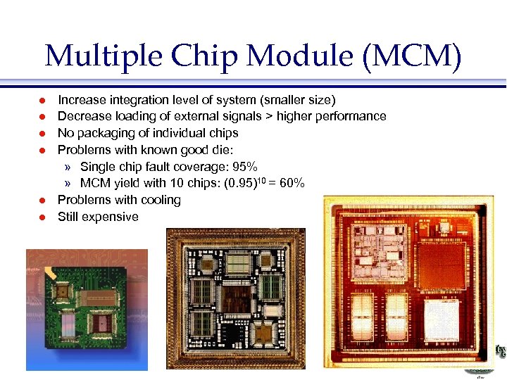
Multiple Chip Module (MCM) l l l Increase integration level of system (smaller size) Decrease loading of external signals > higher performance No packaging of individual chips Problems with known good die: » Single chip fault coverage: 95% » MCM yield with 10 chips: (0. 95)10 = 60% Problems with cooling Still expensive EE 415 VLSI Design
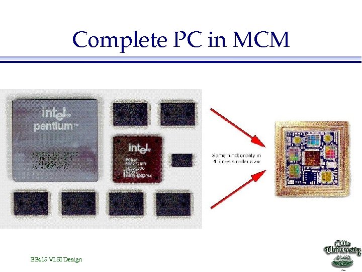
Complete PC in MCM EE 415 VLSI Design
584940ae3236287c414f2941be04f246.ppt