89ae622ced15f8372e03c3477d6b7605.ppt
- Количество слайдов: 72
 MAMAS – Computer Architecture PC Structure and Peripherals Dr. Lihu Rappoport 1/2005 1 pc structure
 Memory Lihu Rappoport 1/2005 2 pc structure
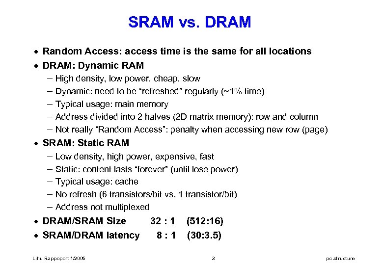 SRAM vs. DRAM · Random Access: access time is the same for all locations · DRAM: Dynamic RAM – High density, low power, cheap, slow – Dynamic: need to be “refreshed” regularly (~1% time) – Typical usage: main memory – Address divided into 2 halves (2 D matrix memory): row and column – Not really “Random Access”: penalty when accessing new row (page) · SRAM: Static RAM – Low density, high power, expensive, fast – Static: content lasts “forever” (until lose power) – Typical usage: cache – No refresh (6 transistors/bit vs. 1 transistor/bit) – Address not multiplexed · DRAM/SRAM Size 32 : 1 (512: 16) · SRAM/DRAM latency 8 : 1 (30: 3. 5) Lihu Rappoport 1/2005 3 pc structure
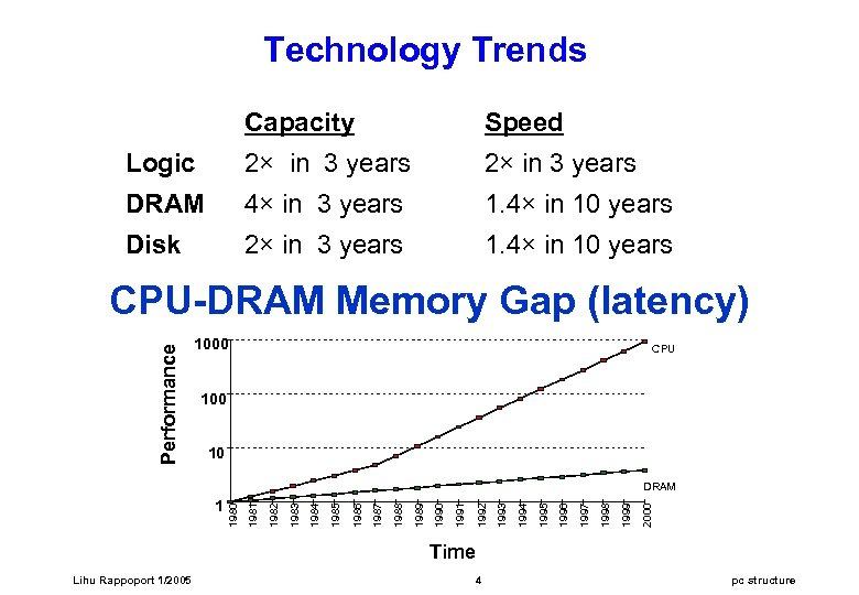 Technology Trends Capacity Speed Logic 2× in 3 years DRAM 4× in 3 years 1. 4× in 10 years Disk 2× in 3 years 1. 4× in 10 years Performance CPU-DRAM Memory Gap (latency) 1000 CPU 100 10 2000 1999 1998 1997 1996 1995 1994 1993 1992 1991 1990 1989 1988 1987 1986 1985 1984 1983 1982 1981 1 1980 DRAM Time Lihu Rappoport 1/2005 4 pc structure
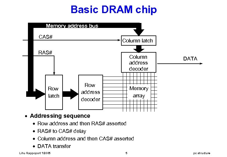 Basic DRAM chip Memory address bus CAS# Column latch RAS# Row latch Column address decoder Row address decoder DATA Memory array · Addressing sequence · · Row address and then RAS# asserted RAS# to CAS# delay Column address and then CAS# asserted DATA transfer Lihu Rappoport 1/2005 5 pc structure
![Addressing sequence Precharge delay t. RAC–Access time RAS# RAS/CAS delay CAS# A[0: 7] X Addressing sequence Precharge delay t. RAC–Access time RAS# RAS/CAS delay CAS# A[0: 7] X](https://present5.com/presentation/89ae622ced15f8372e03c3477d6b7605/image-6.jpg) Addressing sequence Precharge delay t. RAC–Access time RAS# RAS/CAS delay CAS# A[0: 7] X Row i X Col n Row j CL - CAS latency Data n · Access sequence · Put row address on data bus and assert RAS# · Wait for RAS# to CAS# delay (t. RCD) · Put column address on data bus and assert CAS# · DATA transfer · Precharge Lihu Rappoport 1/2005 6 pc structure
Addressing sequence Precharge delay t. RAC–Access time RAS# RAS/CAS delay CAS# A[0: 7] X Row i X Col n Row j CL - CAS latency Data n · Access sequence · Put row address on data bus and assert RAS# · Wait for RAS# to CAS# delay (t. RCD) · Put column address on data bus and assert CAS# · DATA transfer · Precharge Lihu Rappoport 1/2005 6 pc structure
![Basic SDRAM controller A[20: 23] Chip address select decoder Time delay gen. RAS# CAS# Basic SDRAM controller A[20: 23] Chip address select decoder Time delay gen. RAS# CAS#](https://present5.com/presentation/89ae622ced15f8372e03c3477d6b7605/image-7.jpg) Basic SDRAM controller A[20: 23] Chip address select decoder Time delay gen. RAS# CAS# Select A[10: 19] A[0: 9] D[0: 7] address mux Memory address bus DRAM R/W# · DRAM data must be periodically refreshed – Needed to keep data correct – DRAM refresh is done by the DRAM controller, using refresh counter Lihu Rappoport 1/2005 7 pc structure
Basic SDRAM controller A[20: 23] Chip address select decoder Time delay gen. RAS# CAS# Select A[10: 19] A[0: 9] D[0: 7] address mux Memory address bus DRAM R/W# · DRAM data must be periodically refreshed – Needed to keep data correct – DRAM refresh is done by the DRAM controller, using refresh counter Lihu Rappoport 1/2005 7 pc structure
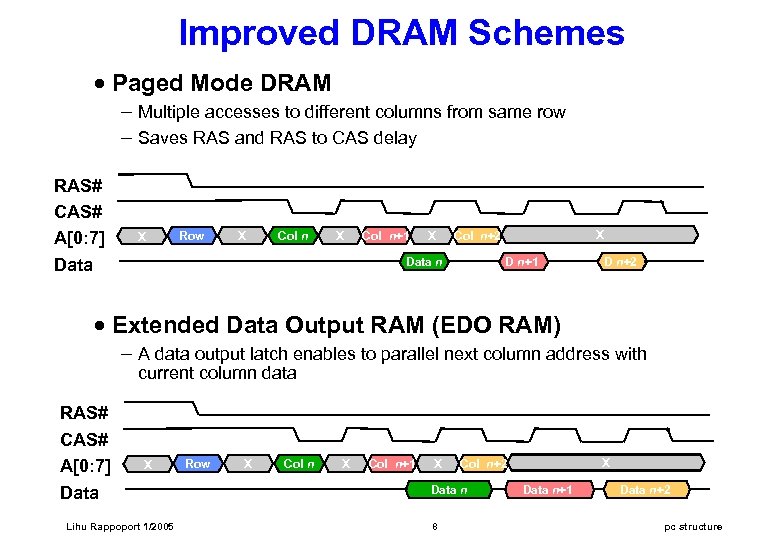 Improved DRAM Schemes · Paged Mode DRAM – Multiple accesses to different columns from same row – Saves RAS and RAS to CAS delay RAS# CAS# A[0: 7] X Row X Col n X Data Col n+1 X X Col n+2 Data n D n+1 D n+2 · Extended Data Output RAM (EDO RAM) – A data output latch enables to parallel next column address with current column data RAS# CAS# A[0: 7] X Data Lihu Rappoport 1/2005 Row X Col n+1 X Data n 8 X Col n+2 Data n+1 Data n+2 pc structure
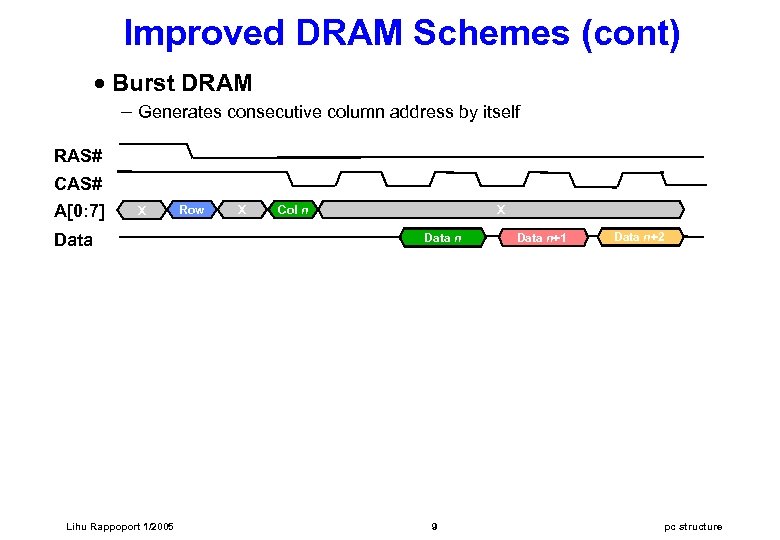 Improved DRAM Schemes (cont) · Burst DRAM – Generates consecutive column address by itself RAS# CAS# A[0: 7] X Data Lihu Rappoport 1/2005 Row X Col n X Data n 9 Data n+1 Data n+2 pc structure
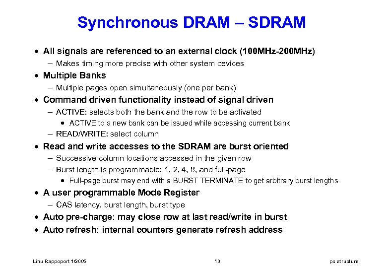 Synchronous DRAM – SDRAM · All signals are referenced to an external clock (100 MHz-200 MHz) – Makes timing more precise with other system devices · Multiple Banks – Multiple pages open simultaneously (one per bank) · Command driven functionality instead of signal driven – ACTIVE: selects both the bank and the row to be activated · ACTIVE to a new bank can be issued while accessing current bank – READ/WRITE: select column · Read and write accesses to the SDRAM are burst oriented – Successive column locations accessed in the given row – Burst length is programmable: 1, 2, 4, 8, and full-page · Full-page burst may end with a BURST TERMINATE to get arbitrary burst lengths · A user programmable Mode Register – CAS latency, burst length, burst type · Auto pre-charge: may close row at last read/write in burst · Auto refresh: internal counters generate refresh address Lihu Rappoport 1/2005 10 pc structure
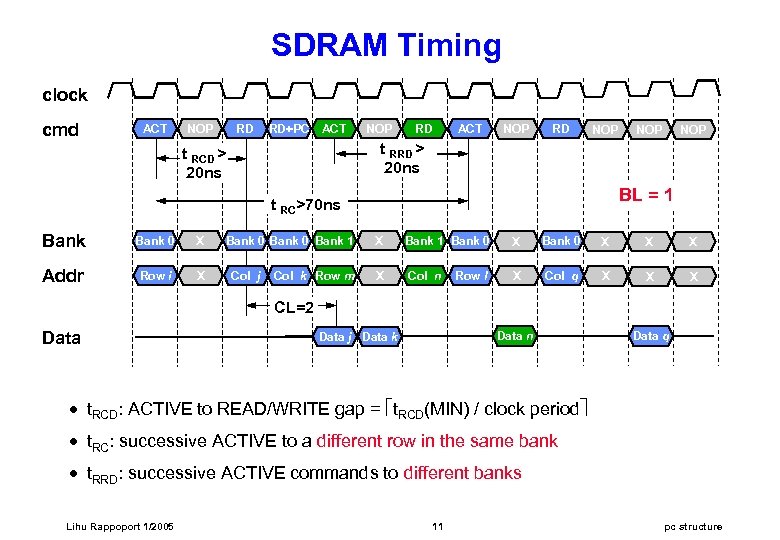 SDRAM Timing clock cmd ACT NOP RD RD+PC ACT NOP RD NOP t RRD > 20 ns t RCD > 20 ns BL = 1 t RC>70 ns Bank 0 X Addr Row i X NOP Bank 0 Bank 1 Col j Col k Row m X X Bank 1 Bank 0 X X X Row l X Col q X X X Col n CL=2 Data n Data j Data k Data q · t. RCD: ACTIVE to READ/WRITE gap = t. RCD(MIN) / clock period · t. RC: successive ACTIVE to a different row in the same bank · t. RRD: successive ACTIVE commands to different banks Lihu Rappoport 1/2005 11 pc structure
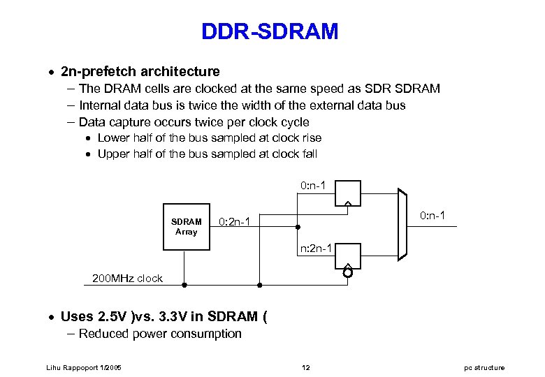 DDR-SDRAM · 2 n-prefetch architecture – The DRAM cells are clocked at the same speed as SDRAM – Internal data bus is twice the width of the external data bus – Data capture occurs twice per clock cycle · Lower half of the bus sampled at clock rise · Upper half of the bus sampled at clock fall 0: n-1 SDRAM Array 0: n-1 0: 2 n-1 n: 2 n-1 200 MHz clock · Uses 2. 5 V )vs. 3. 3 V in SDRAM ( – Reduced power consumption Lihu Rappoport 1/2005 12 pc structure
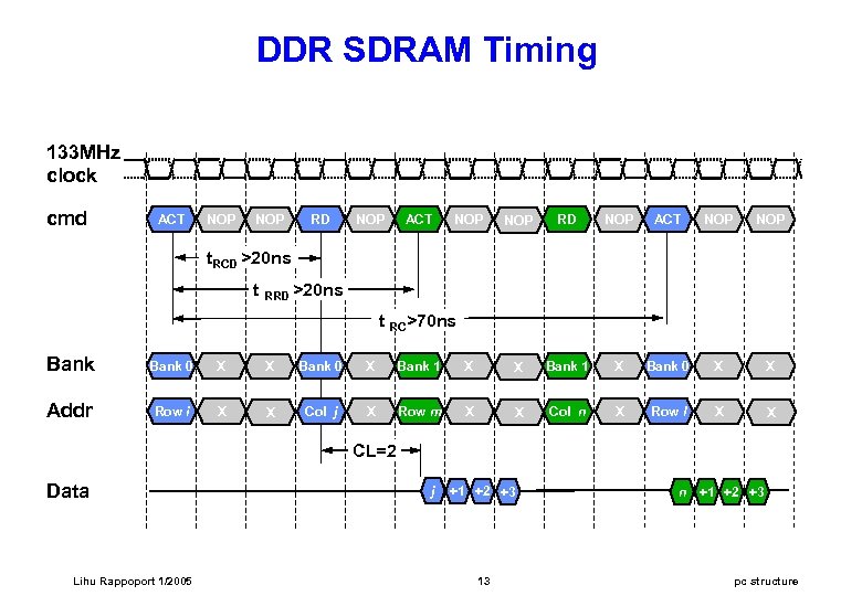 DDR SDRAM Timing 133 MHz clock cmd ACT NOP NOP RD NOP ACT NOP t. RCD >20 ns t RRD >20 ns t RC>70 ns Bank 0 X X Bank 0 X Bank 1 X Bank 0 X X Addr Row i X X Col j X Row m X X Col n X Row l X X CL=2 Data Lihu Rappoport 1/2005 j +1 +2 +3 13 n +1 +2 +3 pc structure
 DIMMs · DIMM: Dual In-line Memory Module – A small circuit board that holds memory chips · 64 -bit wide data path (72 bit with parity) – Single sided: 9 chips, each with 8 bit data bus · 512 Mbit / chip 8 chips 512 Mbyte per DIMM – Dual sided: 18 chips, each with 4 bit data bus · 256 Mbit / chip 16 chips 512 Mbyte per DIMM Lihu Rappoport 1/2005 14 pc structure
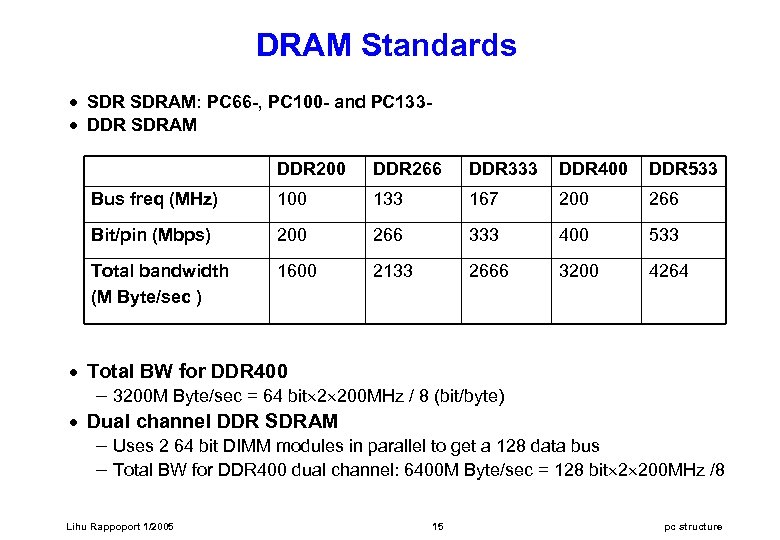 DRAM Standards · SDRAM: PC 66 -, PC 100 - and PC 133· DDR SDRAM DDR 200 DDR 266 DDR 333 DDR 400 DDR 533 Bus freq (MHz) 100 133 167 200 266 Bit/pin (Mbps) 200 266 333 400 533 Total bandwidth (M Byte/sec ) 1600 2133 2666 3200 4264 · Total BW for DDR 400 – 3200 M Byte/sec = 64 bit 2 200 MHz / 8 (bit/byte) · Dual channel DDR SDRAM – Uses 2 64 bit DIMM modules in parallel to get a 128 data bus – Total BW for DDR 400 dual channel: 6400 M Byte/sec = 128 bit 2 200 MHz /8 Lihu Rappoport 1/2005 15 pc structure
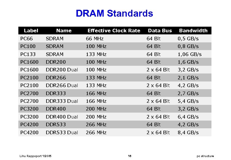 DRAM Standards Label Name Effective Clock Rate Data Bus Bandwidth PC 66 SDRAM 66 MHz 64 Bit 0, 5 GB/s PC 100 SDRAM 100 MHz 64 Bit 0, 8 GB/s PC 133 SDRAM 133 MHz 64 Bit 1, 06 GB/s PC 1600 DDR 200 100 MHz 64 Bit 1, 6 GB/s PC 1600 DDR 200 Dual 100 MHz 2 x 64 Bit 3, 2 GB/s PC 2100 DDR 266 133 MHz 64 Bit 2, 1 GB/s PC 2100 DDR 266 Dual 133 MHz 2 x 64 Bit 4, 2 GB/s PC 2700 DDR 333 166 MHz 64 Bit 2, 7 GB/s PC 2700 DDR 333 Dual 166 MHz 2 x 64 Bit 5, 4 GB/s PC 3200 DDR 400 200 MHz 64 Bit 3, 2 GB/s PC 3200 DDR 400 Dual 200 MHz 2 x 64 Bit 6, 4 GB/s PC 4200 DDR 533 266 MHz 64 Bit 4, 2 GB/s PC 4200 DDR 533 Dual 266 MHz 2 x 64 Bit 8, 4 GB/s Lihu Rappoport 1/2005 16 pc structure
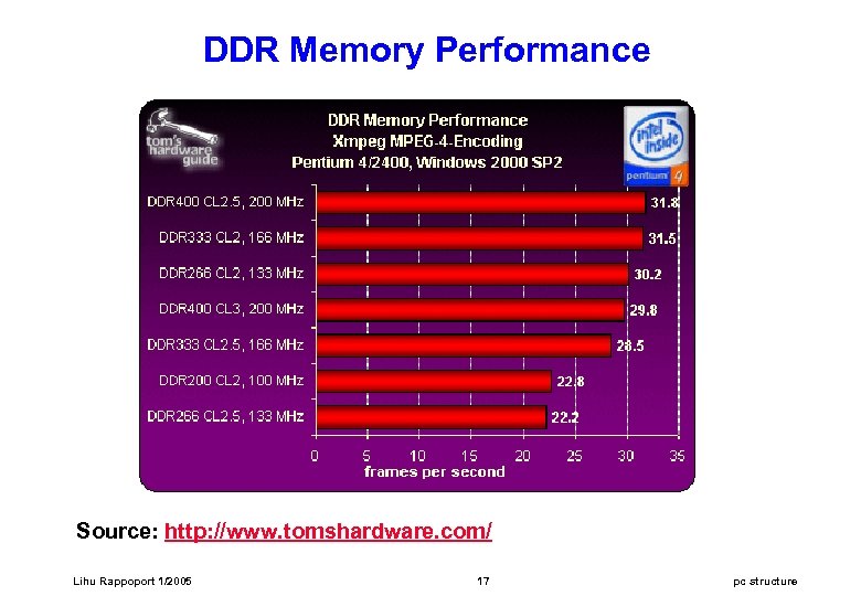 DDR Memory Performance Source: http: //www. tomshardware. com/ Lihu Rappoport 1/2005 17 pc structure
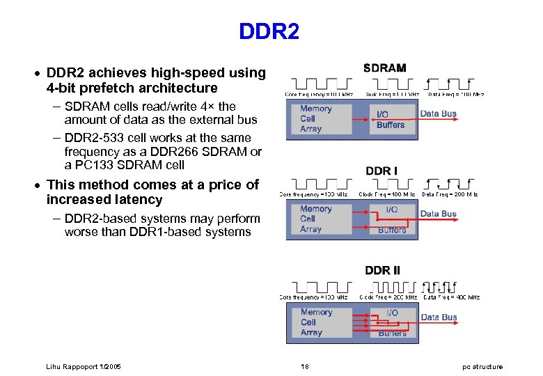 DDR 2 · DDR 2 achieves high-speed using 4 -bit prefetch architecture – SDRAM cells read/write 4× the amount of data as the external bus – DDR 2 -533 cell works at the same frequency as a DDR 266 SDRAM or a PC 133 SDRAM cell · This method comes at a price of increased latency – DDR 2 -based systems may perform worse than DDR 1 -based systems Lihu Rappoport 1/2005 18 pc structure
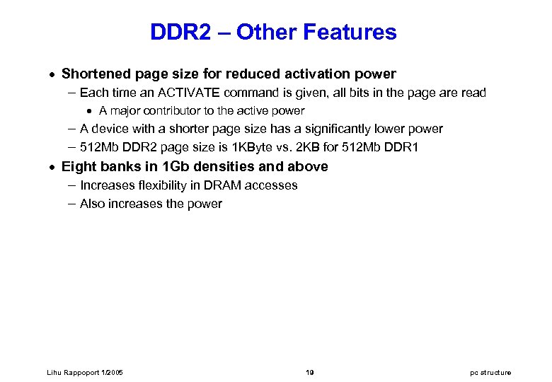 DDR 2 – Other Features · Shortened page size for reduced activation power – Each time an ACTIVATE command is given, all bits in the page are read · A major contributor to the active power – A device with a shorter page size has a significantly lower power – 512 Mb DDR 2 page size is 1 KByte vs. 2 KB for 512 Mb DDR 1 · Eight banks in 1 Gb densities and above – Increases flexibility in DRAM accesses – Also increases the power Lihu Rappoport 1/2005 19 pc structure
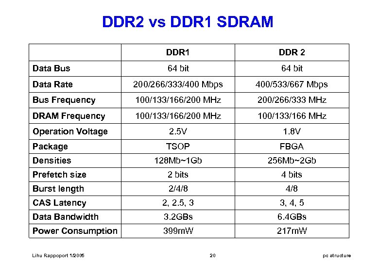 DDR 2 vs DDR 1 SDRAM DDR 1 DDR 2 Data Bus 64 bit Data Rate 200/266/333/400 Mbps 400/533/667 Mbps Bus Frequency 100/133/166/200 MHz 200/266/333 MHz DRAM Frequency 100/133/166/200 MHz 100/133/166 MHz Operation Voltage 2. 5 V 1. 8 V Package TSOP FBGA Densities 128 Mb~1 Gb 256 Mb~2 Gb Prefetch size 2 bits 4 bits Burst length 2/4/8 CAS Latency 2, 2. 5, 3 3, 4, 5 Data Bandwidth 3. 2 GBs 6. 4 GBs Power Consumption 399 m. W 217 m. W Lihu Rappoport 1/2005 20 pc structure
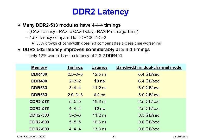 DDR 2 Latency · Many DDR 2 -533 modules have 4 -4 -4 timings – (CAS Latency - RAS to CAS Delay - RAS Precharge Time) – 1. 5× latency compared to DDR 400 2– 3– 2 · 30% growth of bandwidth does not compensates access time worsening · DDR 2 -533 latency improves considerably at 3 -3 -3 timings – only 12% worse than the latency of 2 -3 -2 DDR 400 Memory Timings Latency Bandwidth in dual-channel mode DDR 400 2. 5– 3– 3 12. 5 ns 6. 4 GB/sec DDR 400 2– 3– 2 10 ns 6. 4 GB/sec DDR 533 3– 4– 4 11. 2 ns 8. 5 GB/sec DDR 533 2. 5– 3– 3 9. 4 ns 8. 5 GB/sec DDR 2 -533 5– 5– 5 18. 8 ns 8. 5 GB/sec DDR 2 -533 4– 4– 4 15 ns 8. 5 GB/sec DDR 2 -533 3– 3– 3 11. 2 ns 8. 5 GB/sec DDR 2 -600 5– 5– 5 16. 6 ns 9. 6 GB/sec DDR 2 -600 4– 4– 4 13. 3 ns 9. 6 GB/sec Lihu Rappoport 1/2005 21 pc structure
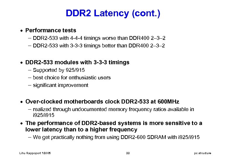 DDR 2 Latency (cont. ) · Performance tests – DDR 2 -533 with 4 -4 -4 timings worse than DDR 400 2– 3– 2 – DDR 2 -533 with 3 -3 -3 timings better than DDR 400 2– 3– 2 · DDR 2 -533 modules with 3 -3 -3 timings – Supported by 925/915 – best choice for enthusiastic users – significant improvement · Over-clocked motherboards clock DDR 2 -533 at 600 MHz – realized through undocumented memory frequency ratios available in i 925/i 915 · The performance of DDR 2 -based systems is more sensitive to a lower latency than to a higher frequency – We get practically nothing from using DDR 2 -600 SDRAM with i 925/i 915 Lihu Rappoport 1/2005 22 pc structure
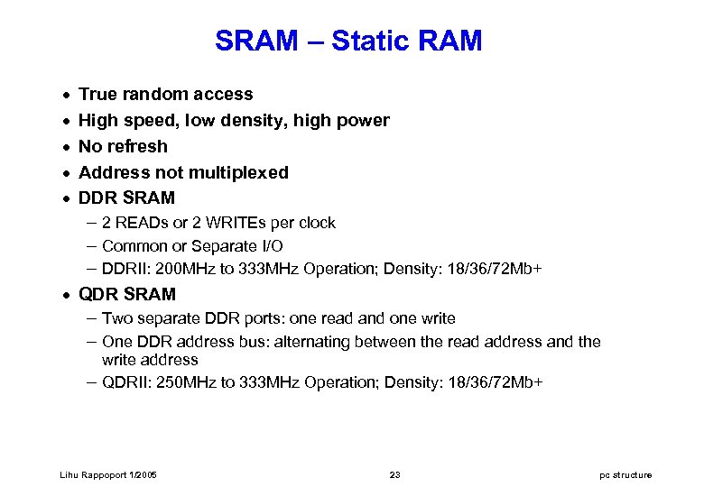 SRAM – Static RAM · · · True random access High speed, low density, high power No refresh Address not multiplexed DDR SRAM – 2 READs or 2 WRITEs per clock – Common or Separate I/O – DDRII: 200 MHz to 333 MHz Operation; Density: 18/36/72 Mb+ · QDR SRAM – Two separate DDR ports: one read and one write – One DDR address bus: alternating between the read address and the write address – QDRII: 250 MHz to 333 MHz Operation; Density: 18/36/72 Mb+ Lihu Rappoport 1/2005 23 pc structure
 Read Only Memory (ROM) · Random Access · Non volatile · PROM – Programmable ROM – Burnt once using special equipment · EPROM – Erasable PROM – Can be erased by exposure to UV, and then reprogrammed · E 2 PROM – Electrically Erasable PROM – Can be erased and reprogrammed on board – Write time (programming) much longer than RAM – Limited number of writes (thousands) Lihu Rappoport 1/2005 24 pc structure
 Flash Memory · Non-volatile, rewritable memory – limited lifespan of around 100, 000 write cycles · Flash drives compared to HD drives: – Smaller size, faster, lighter, noiseless, consume less energy – Withstanding shocks up to 2000 Gs · Equivalent to a 10 foot drop onto concrete -without losing data – Much lower capacity (around 100 MB( – Much more expensive (cost/byte( Lihu Rappoport 1/2005 25 pc structure
 The Motherboard Lihu Rappoport 1/2005 26 pc structure
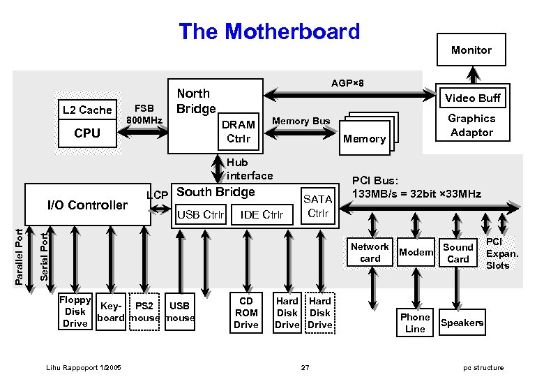 The Motherboard Monitor L 2 Cache FSB 800 MHz AGP× 8 North Bridge Video Buff DRAM Ctrlr CPU Memory Hub interface LCP South Bridge USB Ctrlr IDE Ctrlr SATA Ctrlr Serial Port Parallel Port I/O Controller PCI Bus: 133 MB/s = 32 bit × 33 MHz Network card Floppy USB Key- PS 2 Disk board mouse Drive Lihu Rappoport 1/2005 CD ROM Drive Graphics Adaptor Memory Bus Hard Disk Drive 27 Modem Sound Card Phone Line PCI Expan. Slots Speakers pc structure
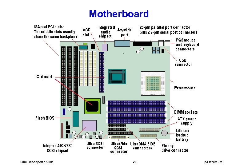 Motherboard Chipset Processor Lihu Rappoport 1/2005 28 pc structure
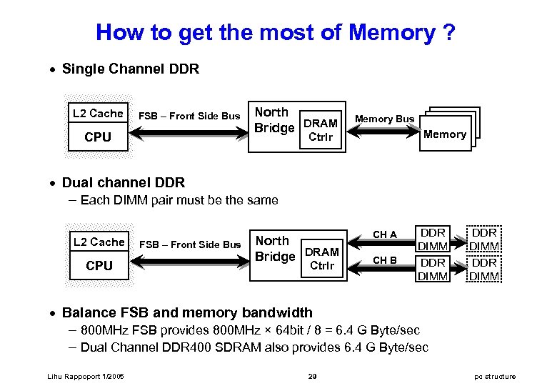 How to get the most of Memory ? · Single Channel DDR L 2 Cache FSB – Front Side Bus CPU North Bridge DRAM Memory Bus Memory Ctrlr · Dual channel DDR – Each DIMM pair must be the same L 2 Cache CPU FSB – Front Side Bus North Bridge DRAM Ctrlr CH A CH B DDR DIMM · Balance FSB and memory bandwidth – 800 MHz FSB provides 800 MHz × 64 bit / 8 = 6. 4 G Byte/sec – Dual Channel DDR 400 SDRAM also provides 6. 4 G Byte/sec Lihu Rappoport 1/2005 29 pc structure
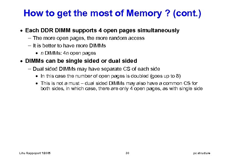 How to get the most of Memory ? (cont. ) · Each DDR DIMM supports 4 open pages simultaneously – The more open pages, the more random access – It is better to have more DIMMs · n DIMMs: 4 n open pages · DIMMs can be single sided or dual sided – Dual sided DIMMs may have separate CS of each side · In this case the number of open pages is doubled (goes up to 8) · This is not a must – dual sided DIMMs may also have a common CS for both sides, in which case, there are only 4 open pages, as with single side Lihu Rappoport 1/2005 30 pc structure
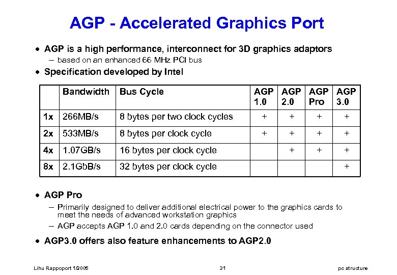 AGP - Accelerated Graphics Port · AGP is a high performance, interconnect for 3 D graphics adaptors – based on an enhanced 66 MHz PCI bus · Specification developed by Intel Bandwidth Bus Cycle AGP AGP 1. 0 2. 0 Pro 3. 0 1 x 266 MB/s 8 bytes per two clock cycles + + 2 x 533 MB/s 8 bytes per clock cycle + + 4 x 1. 07 GB/s 16 bytes per clock cycle + + + 8 x 2. 1 Gb. B/s 32 bytes per clock cycle + · AGP Pro – Primarily designed to deliver additional electrical power to the graphics cards to meet the needs of advanced workstation graphics – AGP accepts AGP 1. 0 and 2. 0 cards depending on the connector used · AGP 3. 0 offers also feature enhancements to AGP 2. 0 Lihu Rappoport 1/2005 31 pc structure
 USB – Universal Serial Bus · USB 2. 0 – providing 40 times the bandwidth of full-speed USB · High-speed, full-speed, and low-speed USB devices · Enhanced Host Controller Interface (EHCI) controller – Supports high speed USB signaling for data transfers up to 480 Mb/s · Universal Host Controller Interface (UHCI) controllers. – Supports full-speed and low-speed USB signaling · When a device is plugged in, – ICH’s port routing logic differentiates whether a high-speed USB device or a classic USB device is connected – Configures the appropriate UHCI or EHCI to controlthe device Lihu Rappoport 1/2005 32 pc structure
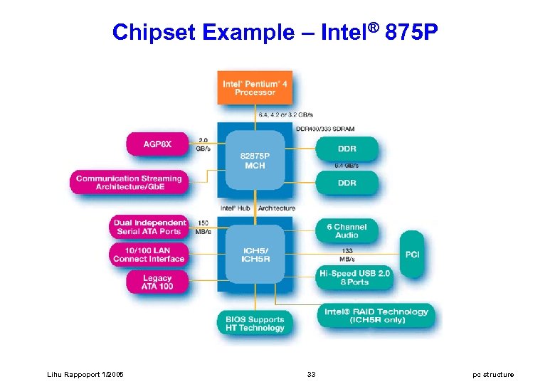 Chipset Example – Intel® 875 P Lihu Rappoport 1/2005 33 pc structure
 PCI Express Lihu Rappoport 1/2005 34 pc structure
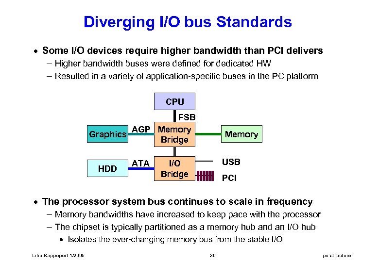 Diverging I/O bus Standards · Some I/O devices require higher bandwidth than PCI delivers – Higher bandwidth buses were defined for dedicated HW – Resulted in a variety of application-specific buses in the PC platform CPU FSB AGP Memory Graphics Bridge HDD ATA Memory USB I/O Bridge PCI · The processor system bus continues to scale in frequency – Memory bandwidths have increased to keep pace with the processor – The chipset is typically partitioned as a memory hub and an I/O hub · Isolates the ever-changing memory bus from the stable I/O Lihu Rappoport 1/2005 35 pc structure
 PCI Limitations vs. Growing Needs · PCI is a multi-drop, parallel bus – Close to its practical limits of performance · Cannot be easily scaled up in frequency or down in voltage – Pushing the limits result in large cost increases for little performance gain · Buses Don’t – scale number of connections – scale physically – scale bandwidth – support multiple traffic types – support high availability · Today’s software applications are more demanding – Streaming data from various video and audio sources are now common – Multiple concurrent transfers at ever-increasing data rates – It is no longer acceptable to treat all data as equal · Streaming data must be processed at real-time Lihu Rappoport 1/2005 36 pc structure
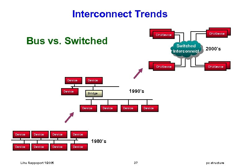 Interconnect Trends Bus vs. Switched Device CPU/Device 1990’s Bridge Device 2000’s Device CPU/Device Switched Interconnect Device CPU/Device Device 1980’s Device Lihu Rappoport 1/2005 Device 37 pc structure
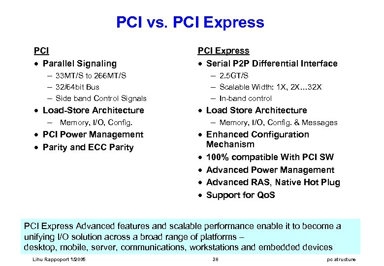 PCI vs. PCI Express PCI · Parallel Signaling – 33 MT/S to 266 MT/S – 32/64 bit Bus – Side band Control Signals · Load-Store Architecture – Memory, I/O, Config. · PCI Power Management · Parity and ECC Parity PCI Express · Serial P 2 P Differential Interface – 2. 5 GT/S – Scalable Width: 1 X, 2 X… 32 X – In-band control · Load Store Architecture – Memory, I/O, Config. & Messages · Enhanced Configuration Mechanism · 100% compatible With PCI SW · Advanced Power Management · Advanced RAS, Native Hot Plug · Support for Qo. S PCI Express Advanced features and scalable performance enable it to become a unifying I/O solution across a broad range of platforms – desktop, mobile, server, communications, workstations and embedded devices Lihu Rappoport 1/2005 38 pc structure
 PCI Express Architecture · SW layers generate read and write requests – Transported by the transaction layer to the I/O devices – Using a packet-based, split-transaction protocol · The link layer adds sequence numbers and CRC to these packets – Create a highly reliable data transfer mechanism · The basic physical layer consists of a dual-simplex channel – Implemented as a transmit pair and a receive pair · The initial speed of 2. 5 Giga transfers/second/direction provides a 200 MB/s communications channel – close to twice the classic PCI data rate Lihu Rappoport 1/2005 39 pc structure
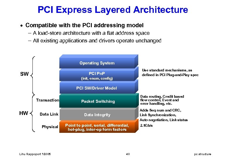 PCI Express Layered Architecture · Compatible with the PCI addressing model – A load-store architecture with a flat address space – All existing applications and drivers operate unchanged Operating System SW Use standard mechanisms, as defined in PCI Plug-and-Play spec PCI Pn. P (init, enum, config) PCI SW/Driver Model Transaction HW Data routing, Credit based flow control, Event and error handling, etc. Packet Switching Adds Seq num and CRC, Link Synchronization, Auto negotiation, Link status Data Link Data Integrity Physical Point to point, serial, differential, hot-plug, inter-op form factors Lihu Rappoport 1/2005 40 2. 5 Gb/s pc structure
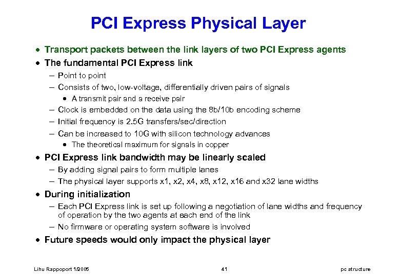 PCI Express Physical Layer · Transport packets between the link layers of two PCI Express agents · The fundamental PCI Express link – Point to point – Consists of two, low-voltage, differentially driven pairs of signals · A transmit pair and a receive pair – Clock is embedded on the data using the 8 b/10 b encoding scheme – Initial frequency is 2. 5 G transfers/sec/direction – Can be increased to 10 G with silicon technology advances · The theoretical maximum for signals in copper · PCI Express link bandwidth may be linearly scaled – By adding signal pairs to form multiple lanes – The physical layer supports x 1, x 2, x 4, x 8, x 12, x 16 and x 32 lane widths · During initialization – Each PCI Express link is set up following a negotiation of lane widths and frequency of operation by the two agents at each end of the link – No firmware or operating system software is involved · Future speeds would only impact the physical layer Lihu Rappoport 1/2005 41 pc structure
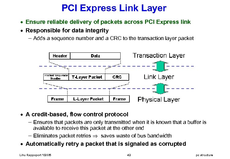 PCI Express Link Layer · Ensure reliable delivery of packets across PCI Express link · Responsible for data integrity – Adds a sequence number and a CRC to the transaction layer packet · A credit-based, flow control protocol – Ensures that packets are only transmitted when it is known that a buffer is available to receive this packet at the other end – Eliminates packet retries saves waste of bus bandwidth · Automatically retry a packet that is signaled as corrupted Lihu Rappoport 1/2005 42 pc structure
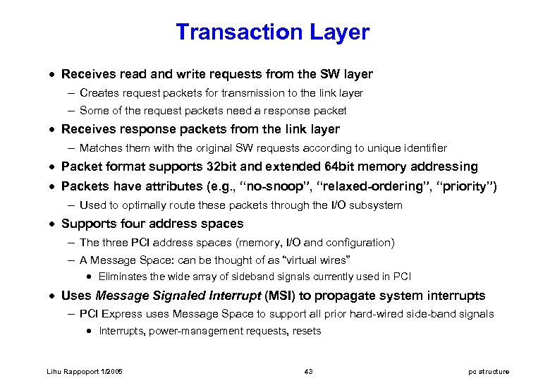 Transaction Layer · Receives read and write requests from the SW layer – Creates request packets for transmission to the link layer – Some of the request packets need a response packet · Receives response packets from the link layer – Matches them with the original SW requests according to unique identifier · Packet format supports 32 bit and extended 64 bit memory addressing · Packets have attributes (e. g. , “no-snoop”, “relaxed-ordering”, “priority”) – Used to optimally route these packets through the I/O subsystem · Supports four address spaces – The three PCI address spaces (memory, I/O and configuration) – A Message Space: can be thought of as “virtual wires” · Eliminates the wide array of sideband signals currently used in PCI · Uses Message Signaled Interrupt (MSI) to propagate system interrupts – PCI Express uses Message Space to support all prior hard-wired side-band signals · Interrupts, power-management requests, resets Lihu Rappoport 1/2005 43 pc structure
 Software Layers · PCI Express Software compatibility – Initialization, or enumeration: · PCI has a robust initialization model: the OS can discover all add-in HW devices present and then allocate system resources, such as memory, I/O space and interrupts, to create an optimal system environment · PCI configuration space and the programmability of I/O devices are key concepts that are unchanged within the PCI Express Architecture; · All operating systems will be able to boot without modification on a PCI Express-based platform – Run-time SW model · PCI uses a load-store, shared memory model · Maintained by PCI Express © All existing software executes unchanged – PCI Express is SW compatible with all existing PCI-based SW · Enable smooth integration within future systems. · New software may use new capabilities Lihu Rappoport 1/2005 44 pc structure
 Mechanical Form Factors · Evolutionary Design – Replace AGP and PCI cards – PCI Express add-in cards co-exist with PCI-form factor boards – Use a new connector placed alongside the existing PCI or AGP connector in the area previously occupied by those type of connectors · PCMCIA announced the development of Express. Card™ – Integrated desktop and mobile external expansion – The next evolution of the PC Card · Smaller form factor · Faster performance Lihu Rappoport 1/2005 45 pc structure
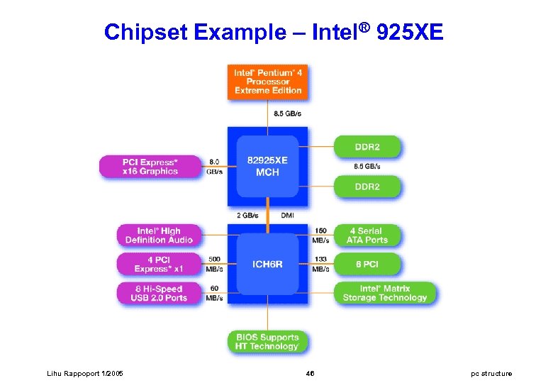 Chipset Example – Intel® 925 XE Lihu Rappoport 1/2005 46 pc structure
 Intel® 925 XE · Optimized for Hyper-Threading Technology · Front side bus – 1066 -and 800 MHz FSB – Dual-channel DDR 2 533 memory – Up to 8. 53 GB/s memory bandwidth – Up to a maximum of 4 GB of RAM · PCI Express* – Up to 4 GB/s per direction for graphics bandwidth – Up to 500 MB/s concurrent data transfers for I/O · Intel® Matrix Storage Technology – Integrated Raid 0 and Raid 1 capabilities using the latest SATA interface · Intel® High Definition Audio Technology – Eight independent DMA audio engines · Enable multiple separate, simultaneous audio streams – Supports 7. 1 surround sound, Dolby Digital, DTS Lihu Rappoport 1/2005 47 pc structure
 Hard Disk Lihu Rappoport 1/2005 48 pc structure
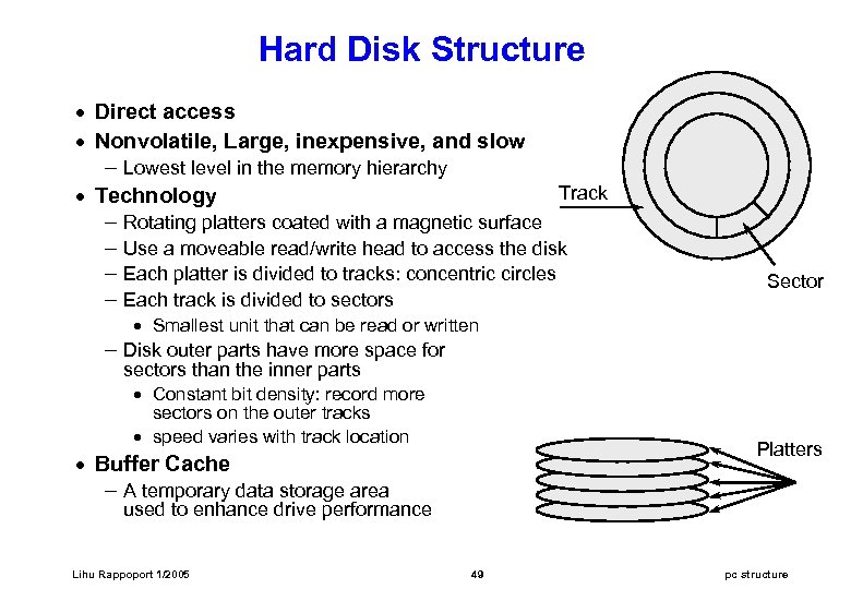 Hard Disk Structure · Direct access · Nonvolatile, Large, inexpensive, and slow – Lowest level in the memory hierarchy Track · Technology – Rotating platters coated with a magnetic surface – Use a moveable read/write head to access the disk – Each platter is divided to tracks: concentric circles – Each track is divided to sectors · Smallest unit that can be read or written – Disk outer parts have more space for sectors than the inner parts · Constant bit density: record more sectors on the outer tracks · speed varies with track location · Buffer Cache – A temporary data storage area Sector Platters used to enhance drive performance Lihu Rappoport 1/2005 49 pc structure
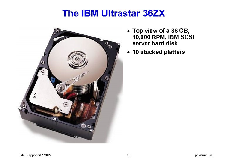 The IBM Ultrastar 36 ZX · Top view of a 36 GB, 10, 000 RPM, IBM SCSI server hard disk · 10 stacked platters Lihu Rappoport 1/2005 50 pc structure
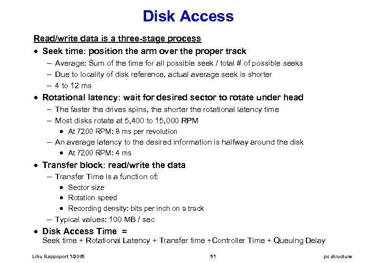 Disk Access Read/write data is a three-stage process · Seek time: position the arm over the proper track – Average: Sum of the time for all possible seek / total # of possible seeks – Due to locality of disk reference, actual average seek is shorter – 4 to 12 ms · Rotational latency: wait for desired sector to rotate under head – The faster the drives spins, the shorter the rotational latency time – Most disks rotate at 5, 400 to 15, 000 RPM · At 7200 RPM: 8 ms per revolution – An average latency to the desired information is halfway around the disk · At 7200 RPM: 4 ms · Transfer block: read/write the data – Transfer Time is a function of: · Sector size · Rotation speed · Recording density: bits per inch on a track – Typical values: 100 MB / sec · Disk Access Time = Seek time + Rotational Latency + Transfer time +Controller Time + Queuing Delay Lihu Rappoport 1/2005 51 pc structure
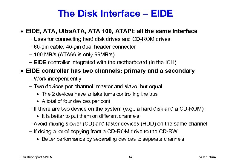 The Disk Interface – EIDE · EIDE, ATA, Ultra. ATA, ATA 100, ATAPI: all the same interface – Uses for connecting hard disk drives and CD-ROM drives – 80 -pin cable, 40 -pin dual header connector – 100 MB/s (ATA 66 is only 66 MB/s) – EIDE controller integrated with the motherboard (in the ICH) · EIDE controller has two channels: primary and a secondary – Work independently – Two devices per channel: master and slave, but equal · The 2 devices have to take turns controlling the bus · A total of four devices per cont – If there are two device on the system (e. g. , a hard disk and a CD-ROM) · It is better to put them on different channels – Avoid mixing slower (CD) and faster devices (HDD) on the same channel – If doing a lot of copying from a CD-ROM drive to the CD-RW · Better performance by separating devices to separate channels Lihu Rappoport 1/2005 52 pc structure
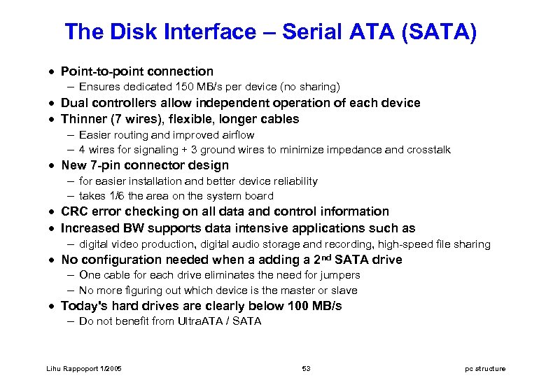 The Disk Interface – Serial ATA (SATA) · Point-to-point connection – Ensures dedicated 150 MB/s per device (no sharing) · Dual controllers allow independent operation of each device · Thinner (7 wires), flexible, longer cables – Easier routing and improved airflow – 4 wires for signaling + 3 ground wires to minimize impedance and crosstalk · New 7 -pin connector design – for easier installation and better device reliability – takes 1/6 the area on the system board · CRC error checking on all data and control information · Increased BW supports data intensive applications such as – digital video production, digital audio storage and recording, high-speed file sharing · No configuration needed when a adding a 2 nd SATA drive – One cable for each drive eliminates the need for jumpers – No more figuring out which device is the master or slave · Today's hard drives are clearly below 100 MB/s – Do not benefit from Ultra. ATA / SATA Lihu Rappoport 1/2005 53 pc structure
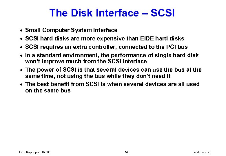 The Disk Interface – SCSI · · Small Computer System Interface SCSI hard disks are more expensive than EIDE hard disks SCSI requires an extra controller, connected to the PCI bus In a standard environment, the performance of single hard disk won’t improve much from the SCSI interface · The power of SCSI is that several devices can use the bus at the same time, not using the bus while they don’t need it · The best benefit from SCSI is when several devices are all used on the same bus Lihu Rappoport 1/2005 54 pc structure
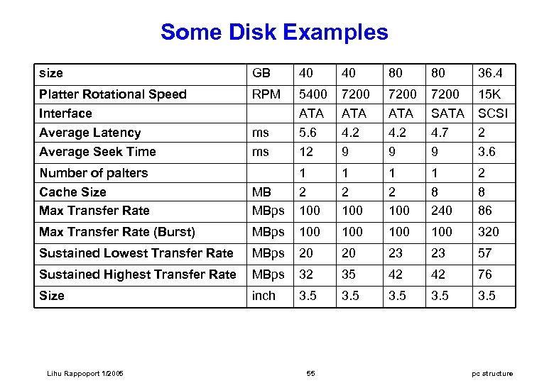 Some Disk Examples size GB 40 40 80 80 36. 4 Platter Rotational Speed Interface Average Latency RPM ms 5400 ATA 5. 6 7200 ATA 4. 2 7200 SATA 4. 7 15 K SCSI 2 Average Seek Time ms 12 9 9 9 3. 6 Number of palters Cache Size Max Transfer Rate MB MBps 1 2 100 1 8 240 2 8 86 Max Transfer Rate (Burst) MBps 100 100 320 Sustained Lowest Transfer Rate MBps 20 23 57 Sustained Highest Transfer Rate MBps 32 35 42 42 76 Size inch 3. 5 3. 5 Lihu Rappoport 1/2005 55 pc structure
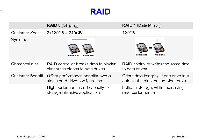 RAID 0 (Striping) Customer Sees: RAID 1 (Data Mirror) 2 x 120 GB = 240 GB 120 GB System: Characteristics RAID controller breaks data to blocks; distributes pieces to both drives Customer Benefit Offers performance benefits over a single hard drive configuration High performance and capacity for storage intensive applications Lihu Rappoport 1/2005 RAID controller writes the same data to both drives Offers data integrity: if one drive fails, data is still intact on the other drive Failsafe storage, while increasing read performance 56 pc structure
 CDROM / DVD Drive · Read speed (max) – Compared to the speed of an audio CD or a video DVD · Write speed · Re-write speed · Capacity 700 MB(CD), 4. 7 GB (DVD) · Interface: EIDE/ATAPI · Data transfer rate (max): – CD 48 x : 7. 2 MB/s = 153, 600 B/s x 48 – DVD 16 x: 21 MB/s = 1, 250, 000 B/s x 16 · CD-R: CD-Recordable: can be written once · CD-RW: CD-Re. Writable: can be written/erased many times (up to 1000) Lihu Rappoport 1/2005 57 pc structure
 Monitors Lihu Rappoport 1/2005 58 pc structure
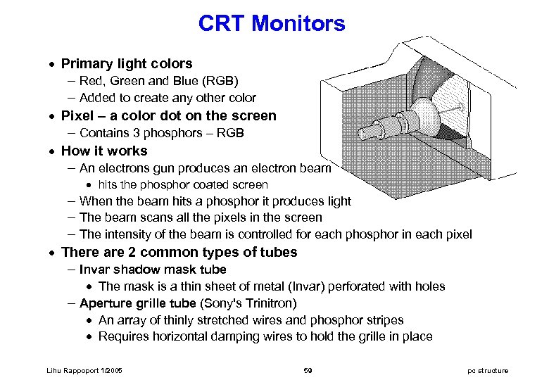 CRT Monitors · Primary light colors – Red, Green and Blue (RGB) – Added to create any other color · Pixel – a color dot on the screen – Contains 3 phosphors – RGB · How it works – An electrons gun produces an electron beam · hits the phosphor coated screen – When the beam hits a phosphor it produces light – The beam scans all the pixels in the screen – The intensity of the beam is controlled for each phosphor in each pixel · There are 2 common types of tubes – Invar shadow mask tube · The mask is a thin sheet of metal (Invar) perforated with holes – Aperture grille tube (Sony's Trinitron) · An array of thinly stretched wires and phosphor stripes · Requires horizontal damping wires to hold the grille in place Lihu Rappoport 1/2005 59 pc structure
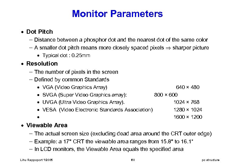 Monitor Parameters · Dot Pitch – Distance between a phosphor dot and the nearest dot of the same color – A smaller dot pitch means more closely spaced pixels sharper picture · Typical dot : 0. 25 mm · Resolution – The number of pixels in the screen – Defined by common Standards · · · VGA (Video Graphics Array) 640 × 480 SVGA (Super Video Graphics array): 800 × 600 UVGA (Ultra Video Graphics Array). 1024 × 768 VESA (Video Electronic Standards Association) 1280 × 1024 1600 × 1200 · Viewable Area – The actual screen size (excluding dead area around the CRT outer edge) – Example: a 17" CRT the viewable area ranges from 15. 8" to 16. 1“ – In LCD monitors, the Viewable Area equals the specified area Lihu Rappoport 1/2005 60 pc structure
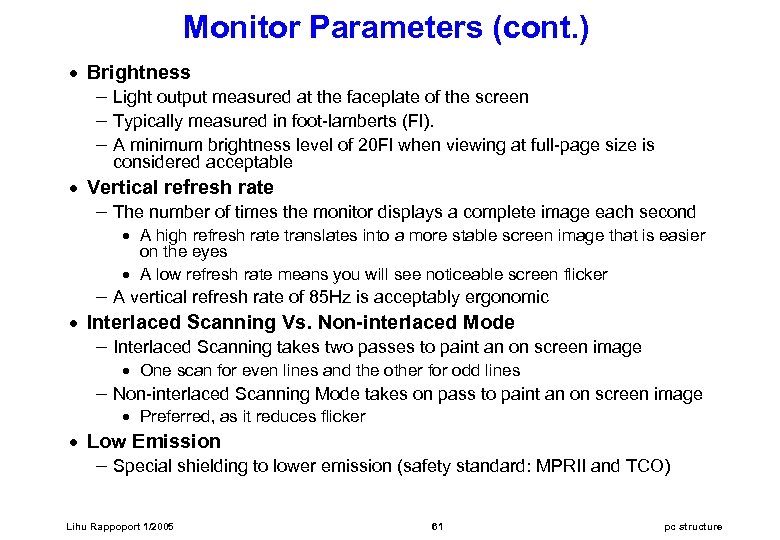 Monitor Parameters (cont. ) · Brightness – Light output measured at the faceplate of the screen – Typically measured in foot-lamberts (Fl). – A minimum brightness level of 20 Fl when viewing at full-page size is considered acceptable · Vertical refresh rate – The number of times the monitor displays a complete image each second · A high refresh rate translates into a more stable screen image that is easier on the eyes · A low refresh rate means you will see noticeable screen flicker – A vertical refresh rate of 85 Hz is acceptably ergonomic · Interlaced Scanning Vs. Non-interlaced Mode – Interlaced Scanning takes two passes to paint an on screen image · One scan for even lines and the other for odd lines – Non-interlaced Scanning Mode takes on pass to paint an on screen image · Preferred, as it reduces flicker · Low Emission – Special shielding to lower emission (safety standard: MPRII and TCO) Lihu Rappoport 1/2005 61 pc structure
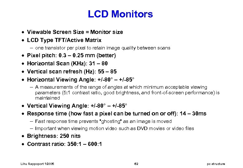 LCD Monitors · Viewable Screen Size = Monitor size · LCD Type TFT/Active Matrix – one transistor per pixel to retain image quality between scans · Pixel pitch: 0. 3 – 0. 25 mm (better) · Horizontal Scan (KHz): 31 – 80 · Vertical scan refresh (Hz): 55 – 85 · Horizontal Viewing Angle: +/-80° – +/-85° – A measurements of the range of angles at which minimum acceptable viewing parameters (5: 1 contrast ratio, good brightness, and front-of-screen performance) is maintained · Vertical Viewing Angle: +/-80° – +/-85° · Response time (how fast a pixel can be turned on or off): 14 – 30 ms – Fast response time prevents "ghosting" as an image is moved – Important when viewing motion video such as DVD movies or video files · Brightness: 250 nits · Contrast ratio: 350: 1 – 600: 1 Lihu Rappoport 1/2005 62 pc structure
 Laser Printers Lihu Rappoport 1/2005 63 pc structure
 Printing Parameters · Printing Speed – Measured in pages per minute (p. p. m) · Personal Printers: 4 - 5 p. p. m. · Office Printers: 8 - 12 p. p. m. · Workgroup Printers: 15 - 30 p. p. m. · Production Printers: 50 p. p. m - 200 p. p. m – Dependant on the complexity of the page · Printing speed of complex pages may be limited by processing time · Printing Resolution – The number of individual dots it can print within a specified area · Typical 600 x 600 dots per square inch (600 DPI) Lihu Rappoport 1/2005 64 pc structure
 Laser Printer Lihu Rappoport 1/2005 65 pc structure
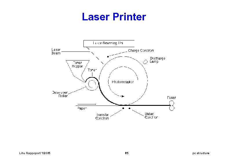
 Laser Printer Structure · The Laser Scanning Assembly is comprised of – Laser: emits a very brief pulse of light for each dot to be printed · No pulse for blank areas – Mirror: deflects the laser beam in the horizontal axis · Carefully synchronized with the laser to position dots along a line · Vertical movement is achieved by moving the photoreceptor – Lens: corrects the beam positioning · Counteract the divergent effect caused by the edges of the photoreceptor being further from the mirror than the center · The drum (photoreceptor): a cylinder with a very smooth surface – Can accept an electrostatic charge, and is discharged by light – Before exposure to the laser beam the drum is charged evenly all over by the charger corotron (a wire carrying a very high voltage) – The laser beam creates a pattern of discharged dots – The drum revolves continuously · The laser scans the drum very fast, so dots appear to be in a straight line – As the drum revolves it passes the developer unit · Charged dots on the drum attract toner from the charged developer roller Lihu Rappoport 1/2005 66 pc structure
 Laser Printer Structure (cont) · Once the paper has passed the drum and attracted the toner – The detac corotron cancels the charge on the paper – Prevent it from sticking to the photoreceptor or other sheets of paper · The drum passes the discharge lamp – Exposes the whole width of the drum to light to erase residual charge · Fuser – Once the toner transferred from the drum it lies on the paper in a very thin coating, with nothing to hold it in place – Paper is heated, by passing between a pair of very hot rollers, so that the plastic toner melts around the fibers of the paper and is "fused" into place · Fixes the toner to the paper permanently Lihu Rappoport 1/2005 67 pc structure
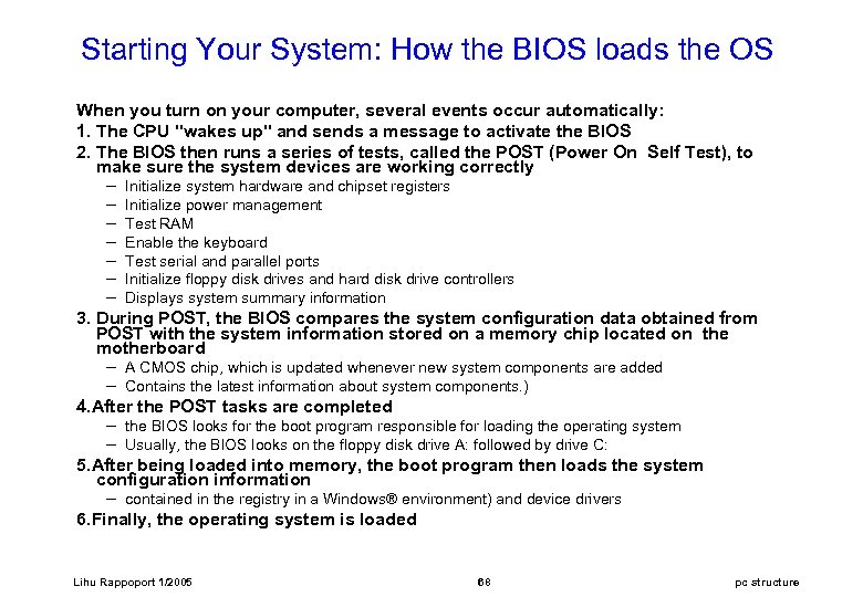 Starting Your System: How the BIOS loads the OS When you turn on your computer, several events occur automatically: 1. The CPU "wakes up" and sends a message to activate the BIOS 2. The BIOS then runs a series of tests, called the POST (Power On Self Test), to make sure the system devices are working correctly – Initialize system hardware and chipset registers – Initialize power management – Test RAM – Enable the keyboard – Test serial and parallel ports – Initialize floppy disk drives and hard disk drive controllers – Displays system summary information 3. During POST, the BIOS compares the system configuration data obtained from POST with the system information stored on a memory chip located on the motherboard – A CMOS chip, which is updated whenever new system components are added – Contains the latest information about system components. ) 4. After the POST tasks are completed – the BIOS looks for the boot program responsible for loading the operating system – Usually, the BIOS looks on the floppy disk drive A: followed by drive C: 5. After being loaded into memory, the boot program then loads the system configuration information – contained in the registry in a Windows® environment) and device drivers 6. Finally, the operating system is loaded Lihu Rappoport 1/2005 68 pc structure
 Back. Up Lihu Rappoport 1/2005 69 pc structure
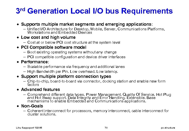 3 rd Generation Local I/O bus Requirements · Supports multiple market segments and emerging applications: – Unified I/O Architecture for Desktop, Mobile, Server, Communications Platforms, Workstations and Embedded Devices · Low cost and high volume – Cost at or below PCI cost structure at the system level · PCI Compatible software model – Boot existing operating systems without any change – PCI compatible configuration and device driver interfaces · Performance: – Scalable performance via frequency and additional lanes – High Bandwidth per Pin. Low overhead. Low latency. · Support multiple platform connection types – Chip-to-chip, board-to-board via connector, docking station and enable new form factors · Advanced features – Comprehend different data types. Power Management. Quality Of Service. Hot Plug and Hot Swap support. Data Integrity and Error Handling. Extensible. Base mechanisms to enable Embedded and Communications applications. · Non-Goals – Coherent interconnect for processors, memory interconnect, cable interconnect for cluster solutions. Lihu Rappoport 1/2005 70 pc structure
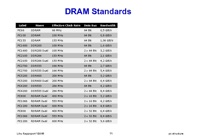 DRAM Standards Label Name Effective Clock Rate Data Bus Bandwidth PC 66 SDRAM 66 MHz 64 Bit 0, 5 GB/s PC 100 SDRAM 100 MHz 64 Bit 0, 8 GB/s PC 133 SDRAM 133 MHz 64 Bit 1, 06 GB/s PC 1600 DDR 200 100 MHz 64 Bit 1, 6 GB/s PC 1600 DDR 200 Dual 100 MHz 2 x 64 Bit 3, 2 GB/s PC 2100 DDR 266 133 MHz 64 Bit 2, 1 GB/s PC 2100 DDR 266 Dual 133 MHz 2 x 64 Bit 4, 2 GB/s PC 2700 DDR 333 166 MHz 64 Bit 2, 7 GB/s PC 2700 DDR 333 Dual 166 MHz 2 x 64 Bit 5, 4 GB/s PC 3200 DDR 400 200 MHz 64 Bit 3, 2 GB/s PC 3200 DDR 400 Dual 200 MHz 2 x 64 Bit 6, 4 GB/s PC 4200 DDR 533 266 MHz 64 Bit 4, 2 GB/s PC 4200 DDR 533 Dual 266 MHz 2 x 64 Bit 8, 4 GB/s PC 800 RDRAM Dual 400 MHz 2 x 16 Bit 3, 2 GB/s PC 1066 RDRAM Dual 533 MHz 2 x 16 Bit 4, 2 GB/s PC 1200 RDRAM Dual 600 MHz 2 x 16 Bit 4, 8 GB/s PC 800 RDRAM Dual 400 MHz 2 x 32 Bit 6, 4 GB/s PC 1066 RDRAM Dual 533 MHz 2 x 32 Bit 8, 4 GB/s PC 1200 RDRAM Dual 600 MHz 2 x 32 Bit 9, 6 GB/s Lihu Rappoport 1/2005 71 pc structure
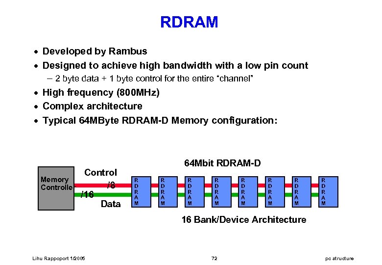 RDRAM · Developed by Rambus · Designed to achieve high bandwidth with a low pin count – 2 byte data + 1 byte control for the entire “channel” · High frequency (800 MHz) · Complex architecture · Typical 64 MByte RDRAM-D Memory configuration: Memory Controller Control /8 /16 Data 64 Mbit RDRAM-D R A M R D R A M R D R A M 16 Bank/Device Architecture Lihu Rappoport 1/2005 72 pc structure


