f556c89ee2d0e623ce6102f57de979ae.ppt
- Количество слайдов: 16
 Main Memory • The last level in the cache – main memory hierarchy is the main memory made of DRAM chips • DRAM parameters (memory latency at the DRAM level): – Access time: time between the read is requested and the desired word arrives – Cycle time: minimum time between requests to memory (cycle time > access time because need for stabilization of address lines) Main Mem. . CSE 471 Autumn 01 1
 DRAM’s • Address lines split into row and column addresses. A read operation consists of: – – – RAS (Row access strobe) CAS (Column access strobe) If device has been precharged, access time = RAS + CAS If not, have to add precharge time RAS, CAS, and Precharge are of the same order of magnitude In DRAM, data needs to be written back after a read, hence cycle time > access time Main Mem. . CSE 471 Autumn 01 2
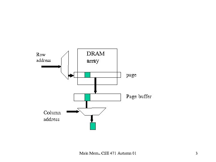 Row address DRAM array page Page buffer Column address Main Mem. . CSE 471 Autumn 01 3
 DRAM and SRAM • D stands for “dynamic” – Each bit is single transistor (plus capacitor; hence the need to rewrite info after a read). – Needs to be recharged periodically. Hence refreshing. All bits in a row can be refreshed concurrently (just read the row). – For each row it takes RAS time to refresh (can lead to up to 5% loss in performance). • S stands for “static” – Uses 6 transistors/bit (some use 4). No refresh and no need to write after read (i. e. , information is not lost by reading; very much like a F/F in a register). Main Mem. . CSE 471 Autumn 01 4
 DRAM vs. SRAM • Cycle time of SRAM 10 to 20 times faster than DRAM • For same technology, capacity of DRAM 5 to 10 times that of SRAM • Hence – Main memory is DRAM – On-chip caches are SRAM – Off-chip caches (it depends) • DRAM growth – Capacity: Factor of 4 every 3 years (60% per year) – Cycle time. Improvement of 20% per generation (7% per year) Main Mem. . CSE 471 Autumn 01 5
 How to Improve Main Memory Bandwidth • It’s easier to improve on bandwidth than on latency • Sending address: can’t be improved (and this is latency) – Although split-transaction bus allows some overlap • Make memory wider (assume monolithic memory) – Sending one address, yields transfer of more than one word if the bus width allows it (and it does nowadays) – But less modularity (buy bigger increments of memory) Main Mem. . CSE 471 Autumn 01 6
 Interleaving (introducing parallelism at the DRAM level) • Memory is organized in banks • Bank i stores all words at address j modulo i • All banks can read a word in parallel – Ideally, number of banks should match (or be a multiple of) the L 2 block size (in words) • Bus does not need to be wider (buffer in the DRAM bank) • Writes to individual banks for different addresses can proceed without waiting for the preceding write to finish (great for write-through caches) Main Mem. . CSE 471 Autumn 01 7
 Banks of Banks • Superbanks interleaved by some bits other than lower bits • Superbanks composed of banks interleaved on low order bits for sequential access • Superbanks allow parallel access to memory – Great for lock-up free caches, for concurrent I/O and for multiprocessors sharing main memory Main Mem. . CSE 471 Autumn 01 8
 Limitations of Interleaving (sequential access) • Number of banks limited by increasing chip capacity – With 1 M x 1 bit chips, it takes 64 x 8 = 512 chips to get 64 MB (easy to put 16 banks of 32 chips) – With 16 M x 1 chips, it takes only 32 chips (only one bank) – More parallelism in using 4 M x 4 chips (32 chips in 4 banks) • In the N * m (N number of MB, m width of bits out of each chip) m is limited by electronic constraints to about 8 or maybe 16. Main Mem. . CSE 471 Autumn 01 9
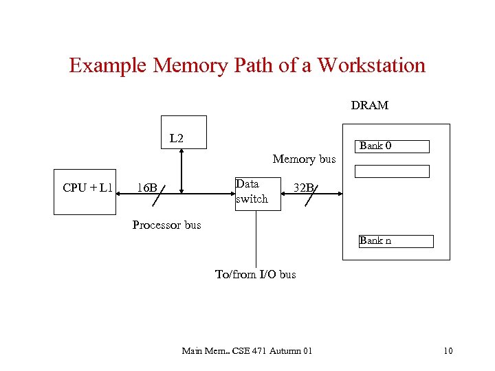 Example Memory Path of a Workstation DRAM L 2 Bank 0 Memory bus CPU + L 1 Data switch 16 B 32 B Processor bus Bank n To/from I/O bus Main Mem. . CSE 471 Autumn 01 10
 Page-mode and Synchronous DRAMs • Introduce a page buffer – In page mode no need for a RAS – But if a miss, need to precharge + RAS + CAS • In SDRAM, same as page-mode but subsequent accesses even faster (burst mode) Main Mem. . CSE 471 Autumn 01 11
 Cached DRAM and Processor in Memory • Put some SRAM on DRAM chip – More flexibility in buffer size than page mode – Can precharge DRAM while accessing SRAM – But fabrication is different hence has not caught up in mass market • Go one step further (1 billion transistors/chip) – Put “simple” processor and SRAM and DRAM on chip – Great bandwidth for processor-memory interface – Cache with very large block size since parallel access to many banks is possible – Can’t have too complex of a processor – Need to invest in new fabs Main Mem. . CSE 471 Autumn 01 12
 Processor in Memory (PIM) • Generality depends on the intended applications • IRAM – Vector processor; data stream apps; low power • Flex. RAM – Memory chip = Host + Simple multiprocessor + banks of DRAM; memory intensive apps. • Active Pages – Co-processor paradigm; reconfigurable logic in memory • FBRAM – Graphics in memory Main Mem. . CSE 471 Autumn 01 13
 Rambus • Specialized memory controller (scheduler), channel, and RDRAM’s • Parallelism and pipelining, e. g. – Independent row , column, and data buses (narrow -- 2 bytes) – Pipelined memory subsystem (several packets/access; packets are 4 cycles = 10 ns) – Parallelism within the RDRAMs (many banks with 4 possible concurrent operations) – Parallelism among RDRAM’s (large number of them) • Great for “streams of data” (Graphics, games) Main Mem. . CSE 471 Autumn 01 14
![Direct Rambus Row [2: 0] Memory controller Column [4: 0] Data [15: 0] Bk Direct Rambus Row [2: 0] Memory controller Column [4: 0] Data [15: 0] Bk](https://present5.com/presentation/f556c89ee2d0e623ce6102f57de979ae/image-15.jpg) Direct Rambus Row [2: 0] Memory controller Column [4: 0] Data [15: 0] Bk 0 Pg 0 Bk 15 Extremely fast bus (400 MHz clock, 800 MHz transfer rate) Great bandwidth for stream data but still high latency for random read/writes Pg 15 RDRAM 0 RDRAM n, n up to 31 Main Mem. . CSE 471 Autumn 01 15
Direct Rambus Row [2: 0] Memory controller Column [4: 0] Data [15: 0] Bk 0 Pg 0 Bk 15 Extremely fast bus (400 MHz clock, 800 MHz transfer rate) Great bandwidth for stream data but still high latency for random read/writes Pg 15 RDRAM 0 RDRAM n, n up to 31 Main Mem. . CSE 471 Autumn 01 15
 Split-transaction Bus • Allows transactions (address, control, data) for different requests to occur simultaneously • Required for efficient Rambus • Great for SMP’s sharing a single bus Main Mem. . CSE 471 Autumn 01 16


