1af46d750417c77425960aafc88ad7a7.ppt
- Количество слайдов: 12
 LOI PROGRESS: JANUARY 2008 AT THE HALL 2 Yoshiro Irie, KEK for the LOI/SH collaboration XII-th Collaboration Meeting Jan 18, 2008@Cosener's House 1
 FLOWER OF THE DAY XII-th Collaboration Meeting Jan 18, 2008@Cosener's House winter cherry! 2
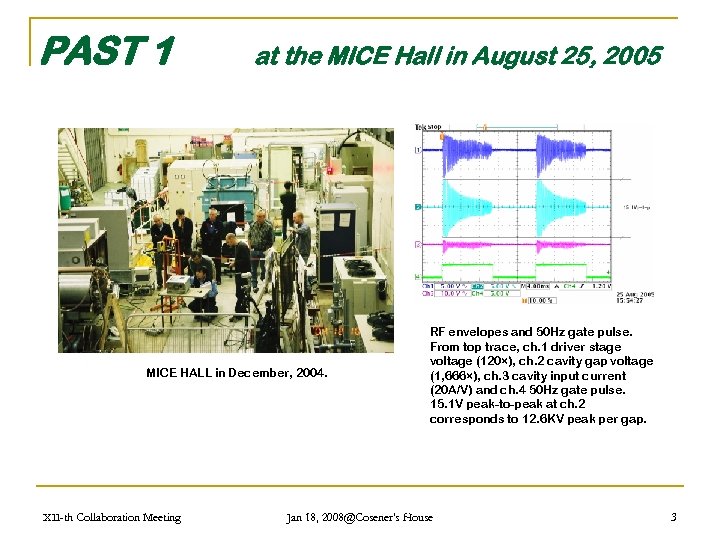 PAST 1 at the MICE Hall in August 25, 2005 MICE HALL in December, 2004. XII-th Collaboration Meeting RF envelopes and 50 Hz gate pulse. From top trace, ch. 1 driver stage voltage (120×), ch. 2 cavity gap voltage (1, 666×), ch. 3 cavity input current (20 A/V) and ch. 4 50 Hz gate pulse. 15. 1 V peak-to-peak at ch. 2 corresponds to 12. 6 KV peak per gap. Jan 18, 2008@Cosener's House 3
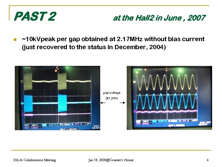 PAST 2 n at the Hall 2 in June , 2007 ~10 k. Vpeak per gap obtained at 2. 17 MHz without bias current (just recovered to the status in December, 2004) gap voltage (X 1, 666) XII-th Collaboration Meeting Jan 18, 2008@Cosener's House 4
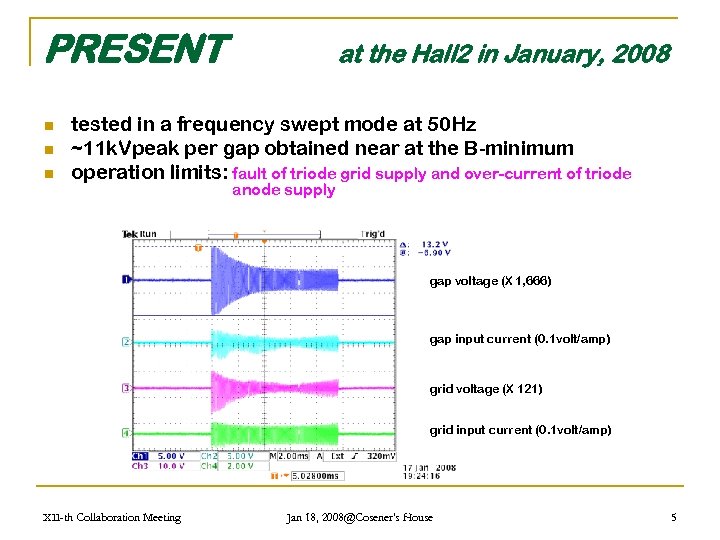 PRESENT n n n at the Hall 2 in January, 2008 tested in a frequency swept mode at 50 Hz ~11 k. Vpeak per gap obtained near at the B-minimum operation limits: fault of triode grid supply and over-current of triode anode supply gap voltage (X 1, 666) gap input current (0. 1 volt/amp) grid voltage (X 121) grid input current (0. 1 volt/amp) XII-th Collaboration Meeting Jan 18, 2008@Cosener's House 5
 REQUIREMENTS PRIOR TO THE EXPERIMENTS n n need a softer step-start, otherwise blow fuses at the H. P. R. F switchboard, increase power capacity of a variac for the screen psu, reinforce the by-pass capacitor at the input of grid bias supply in the LOI, newly install the grid input current monitor, increase the Buck Regulator output power threshold. : All done successfully XII-th Collaboration Meeting Jan 18, 2008@Cosener's House 6
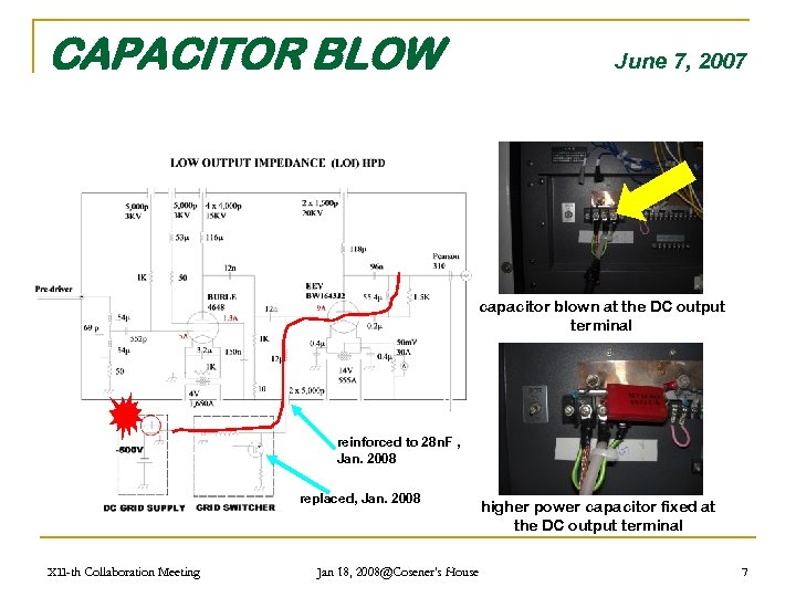 CAPACITOR BLOW June 7, 2007 capacitor blown at the DC output terminal reinforced to 28 n. F , Jan. 2008 replaced, Jan. 2008 XII-th Collaboration Meeting Jan 18, 2008@Cosener's House higher power capacitor fixed at the DC output terminal 7
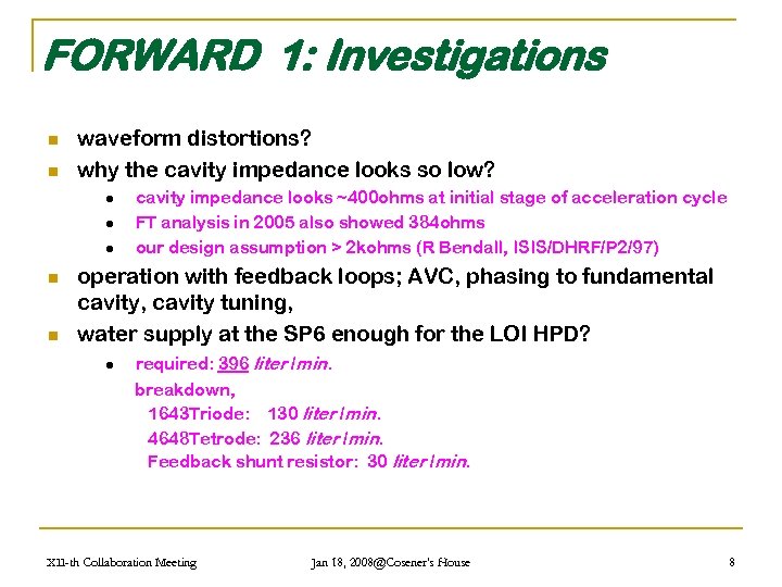 FORWARD 1: Investigations n n waveform distortions? why the cavity impedance looks so low? l l l n n cavity impedance looks ~400 ohms at initial stage of acceleration cycle FT analysis in 2005 also showed 384 ohms our design assumption > 2 kohms (R Bendall, ISIS/DHRF/P 2/97) operation with feedback loops; AVC, phasing to fundamental cavity, cavity tuning, water supply at the SP 6 enough for the LOI HPD? l required: 396 liter /min. breakdown, 1643 Triode: 130 liter /min. 4648 Tetrode: 236 liter /min. Feedback shunt resistor: 30 liter /min. XII-th Collaboration Meeting Jan 18, 2008@Cosener's House 8
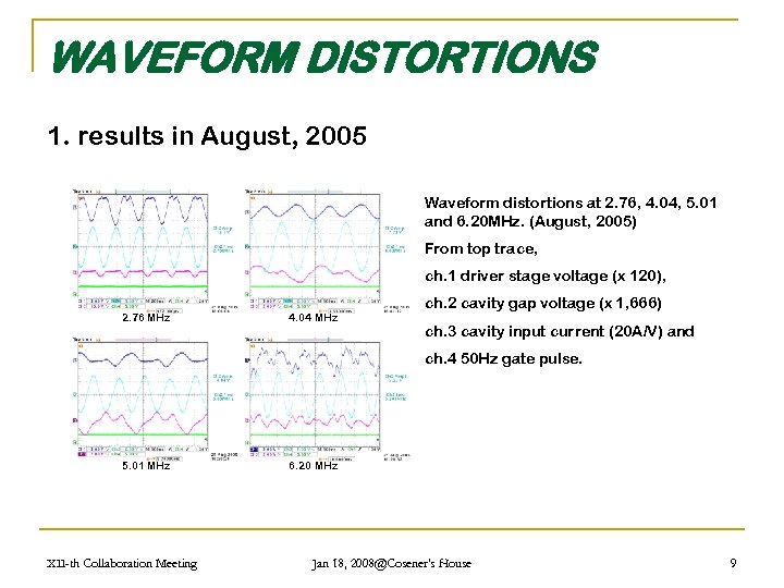 WAVEFORM DISTORTIONS 1. results in August, 2005 Waveform distortions at 2. 76, 4. 04, 5. 01 and 6. 20 MHz. (August, 2005) From top trace, ch. 1 driver stage voltage (x 120), 2. 76 MHz 4. 04 MHz ch. 2 cavity gap voltage (x 1, 666) ch. 3 cavity input current (20 A/V) and ch. 4 50 Hz gate pulse. 5. 01 MHz XII-th Collaboration Meeting 6. 20 MHz Jan 18, 2008@Cosener's House 9
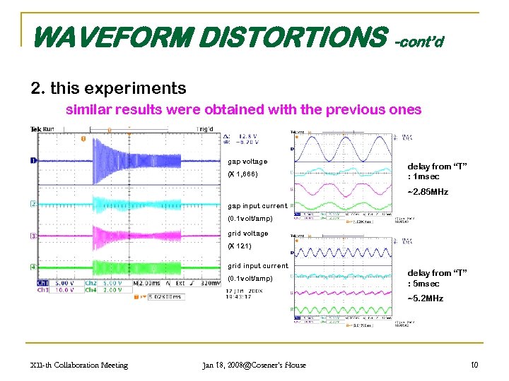 WAVEFORM DISTORTIONS -cont’d 2. this experiments similar results were obtained with the previous ones gap voltage (X 1, 666) delay from “T” : 1 msec ~2. 85 MHz gap input current (0. 1 volt/amp) grid voltage (X 121) grid input current (0. 1 volt/amp) delay from “T” : 5 msec ~5. 2 MHz XII-th Collaboration Meeting Jan 18, 2008@Cosener's House 10
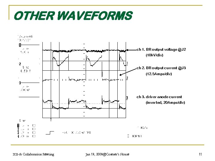 OTHER WAVEFORMS ch 1. BR output voltage @J 2 (10 k. V/div) ch 2. BR output current @J 3 (12. 5 Amps/div) ch 3. driver anode current (inverted, 20 Amps/div) XII-th Collaboration Meeting Jan 18, 2008@Cosener's House 11
 FORWARD 2: to-do-list n n n build a new breakout box at the SP 6, lay cables between breakout boxes in Hall 2 and SP 6, etc. . END XII-th Collaboration Meeting Jan 18, 2008@Cosener's House 12


