

Лекция 12_2011 самоорг.ppt
- Количество слайдов: 49
 Лекция 16. Самоорганизация наноструктур 1. 2. 3. 4. 5. Типы самоорганизации. Физическая самоорганизация Химическая самоорганизация Пленки Ленгмюра-Блоджетт Применение: молекулярная электроника
 Самоорганизация – процесс, при котором молекулы, молекулярные кластеры или коллоидные наночастицы агрегируются в заданную структуру. Bottom-up Физическая СО- спонтанная, вследствие наличия потенциального минимума, силы Ван-дер-Ваальса : рост при эпитаксии, коллоидные частицы (немодифицированные) Химическая СО: коллоидные частицы (модифицированные) агрегирование молекул с использованием дополнительных связей
 Самоорганизация при эпитаксии • Self-organized QDs through epitaxial growth strains – Stranski-Krastanov growth mode (use MBE, MOCVD) • Islands formed on wetting layer due to lattice mismatch (size ~10 s nm) – Disadvantage: size and shape fluctuations, ordering – Control island initiation • Induce local strain, grow on dislocation, vary growth conditions, combine with patterning AFM images of islands epitaxiall grown on Ga. As substrate. (a) In. As islands randomly nucleate. (b) Random distribution of Inx. Ga 1 x. As ring shaped islands. (c) A 2 D lattice of In. As islands on a Ga. As substrate. P. Petroff, A. Lorke, and A. Imamoglu. Epitaxially self-assembled quantum dots. Physics Today, May 2001.
 Химическая самоорганизация 1
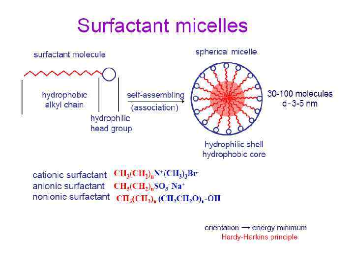
 Коллоидные частицы


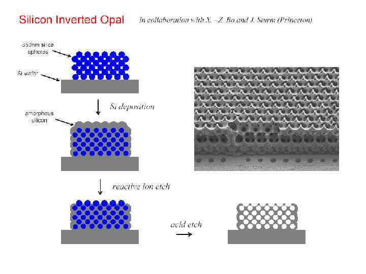
 Формирование опалов Выпадение в осадок Высушивание -> синтетический опал

 Химическая самоорганизация 2
n Sulfur") Самоорганизация тиолов на поверхности золота Au on glass Alkyl chains X (CH 2)n Sulfur S Au X = -CH 3, -OH, -COOH, -SO 3 -, -PO 4 H 2, N+(CH 3)3, -(OCH 2)n. OH, . . . Gold is usually deposited by vacuum evaporation techniques. Electroless gold is also of interest for complex geometries.
Самоорганизация тиолов на поверхности золота Au on glass Alkyl chains X (CH 2)n Sulfur S Au X = -CH 3, -OH, -COOH, -SO 3 -, -PO 4 H 2, N+(CH 3)3, -(OCH 2)n. OH, . . . Gold is usually deposited by vacuum evaporation techniques. Electroless gold is also of interest for complex geometries.
 Ориентация молекулы тиола на поверхности Aliphatic chain within a SAM formed from an alkanethiol on a surface of gold. Directions of transition dipole moments corresponding to C-H stretching modes are shown. The projections of the transition dipole moments along the surface normal (z) are determined by the tilt angle (a) and twist angle (b) of the chain. In this diagram, a = 30 and b = 0.
 SAMs on gold Alkanethiols on single crystals of gold. Open circles represent gold atoms, and shaded circles represent alkyl chains. (a) Au(111). The smaller rhombus shows the Au(111) lattice. The larger rhombus shows a unit mesh with a = b = 4. 97 Å and = 120 (angle between a and b). (b) Au(110). Also shown is a unit mesh with a = b = 4. 99 Å and = 109. 5. (c) Au(100). Also shown is an oblique mesh with a = b = 5. 97 Å and = 95. Camillone et al, J. Chem. Phys. , 1993. Hou, Stroeve et al. , Langmuir 1998.
 Li and Huck, Curr. Op. Solid State and Mat. Science, 2002") Stamping (microcontact printing) Li and Huck, Curr. Op. Solid State and Mat. Science, 2002
Stamping (microcontact printing) Li and Huck, Curr. Op. Solid State and Mat. Science, 2002
 Самоорганизация макромолекул Self-assembly of a double rosette superstructure 19 through the interaction, mediated by hydrogen bonds, of barbiturate 17 with melamine derivative 18 R. N. Reinhoudt, U of Twente, Angew. Chemie, 1996
 3. Ленгмюровские слои • Молекулы нерастворимы в растворе • Молекулы формируют монослой на границе раздела воздух-жидкость • The carbon chain possesses at least 12 Carbons Langmuir Trough Ленгмюровский кристаллизатор
 Пленки Ленгмюра-Блоджетт Подложка микровесы Барьер Liquid Subphase Langmuir Trough
 Пленки Ленгмюра-Блоджетт Молекулы пленки Молекулы растворителя Langmuir Trough
 Langmuir-Blodgett Deposition Film molecule Solvent molecule Langmuir Trough
 Langmuir-Blodgett Deposition Film molecule Solvent molecule Langmuir Trough
 Langmuir-Blodgett Deposition Langmuir Trough
 Langmuir-Blodgett Deposition Langmuir Trough
 Изотерма Pressure Solid phase Liquid phase Gas Phase Area Langmuir Trough
 Langmuir Monolayers : Phase transition isotherm P In the I phase: S L 2 I L 1 L 20 22 G L 40 -70 Molecular Area (A 2/ molecule) G 100
 Langmuir-Blodgett Films X Y Z
 Langmuir monolayers : Characterization Analysis of Film Properties - Thickness measurements - Infrared and Raman Spectroscopy - X-Ray, Electron and Neutron Diffraction - HEELS, etc. Analysis of Surface Properties - Contact angle and Surface tension - Different microscopies: fluorescence, SEM, TEM, STM, AFM, etc. - Non-linear optic techniques
 Multilayer Deposition: Y TO X and Y to Z Transitions
 X, Y AND Z-TYPE DEPOSITION AND TRANSFER RATIO
 MOVING CONTACT LINES: INTERACTING MOLECULAR FORCES
 Colloid Theory applied to LB films • Solid surfaces acquire charge by ionization of surface groups. • An LB film is a 2 -D solid. • At p. Ka of the acid there is a compact layer of divalent cations. • The two films (at air-water and solid-water) films are similar. (Are they not? )
 Non-equilibrium configurations
 Molecular rearrangement under water
 Influence of Cation type
 Effect of film elasticity on transfer ratio
") Применения ленгмюровских пленок • Двумерные слои для исследований • Био-миметика ( «подражание мембранам» ) – Фосфодипидные слои с включениями протеинов • Нелинейная оптика • Сверхплотная магнитная память – Magnetic nano-particles and nano-films • Сегнетоэлектрические слои (PVDF) • Нано-сенсоры – Combination of MEMS and NEMS
Применения ленгмюровских пленок • Двумерные слои для исследований • Био-миметика ( «подражание мембранам» ) – Фосфодипидные слои с включениями протеинов • Нелинейная оптика • Сверхплотная магнитная память – Magnetic nano-particles and nano-films • Сегнетоэлектрические слои (PVDF) • Нано-сенсоры – Combination of MEMS and NEMS
 Applications: Nanosensors
 молекулярная электроника Одноэлектронные приборы Приборы на основе углеродных нанотруб Приборы на основе органических молекул
") ОДНОЭЛЕКТРОННЫЙ ТРАНЗИСТОР (МГУ)
ОДНОЭЛЕКТРОННЫЙ ТРАНЗИСТОР (МГУ)
 ОДНОЭЛЕКТРОННЫЙ МОЛЕКУЛЯРНЫЙ ТРАНЗИСТОР
 Single Electron Molecular Transistor F. Di Salvo and D. Ralph, Cornell University, 2002 ? The two molecules contain a central cobalt atom and differ in their length the shorter of about 2 nm one exhibits less resistance. At low temperature, the longer molecule functions as a single electron transistor, and the shorter molecule exhibits both transistor action and the Kondo effect. ? The electrical characteristis of the transistor can be varied systematically by making chemical changes to the molecule.
 УГЛЕРОДНЫЕ НАНОТРУБКИ ЭТО ВЫСОКОСТАБИЛЬНЫЕПОЛИМЕР, КОТОРЫЕ МОГУТ БЫТЬ ОДНОМЕРНЫМ МЕТАЛЛАМИ ИЛИ ПОЛУПРОВОДНИКАМИ. ИХ ДЛИНУ И ЭЛЕКТРИЧЕСКИЕ СВОЙСТВА МОЖНО ЗАДАВАТЬ, ВАРЬИРУЯ УСЛОВИЯ ИХ СИНТЕЗА.
 Массивы одноэлектронных ключей для саморазвивающейся нейроноподобной сети Такая архитектура позволяет комбинировать высокую плотность CMOS схем (10 8 / см 2 ) с очень высокой плотностью массива одноэлектронных переключателей (до 10 12 /см 2 ), играющих роль синапсов, для создания аналога коры головного мозга на кремниевой пластине (К. Лихарев)
 «Молекулярные» интегральные схемы – интегрирование молекулярного устройства на пооверхности CMOS ИC CMOL circuit (schematically): (a) side view; (b) view from the bottom on the pin/nanowire/molecular subsystem. (The former panel may understood as the cross section of the chip along the line A A shown in the latter panel. ) Fmicro and Fnano are minimum feature sizes (half pitches) of the CMOS and nanowire/molecular subsystems, respectively. Note the incline of the pin array relative to the nanowire array, that enables CMOS pins to contact to each nanowire individually even in the case Fmicro Fnano.