55c865ba121813504e32203c92c9e33c.ppt
- Количество слайдов: 41
 Lecture 5 Optical Lithography
 Intro • For most of microfabrication purposes the process (e. g. additive, subtractive or implantation) has to be applied selectively to particular areas of the wafer: patterning is required; • Predominately done by optical lithography
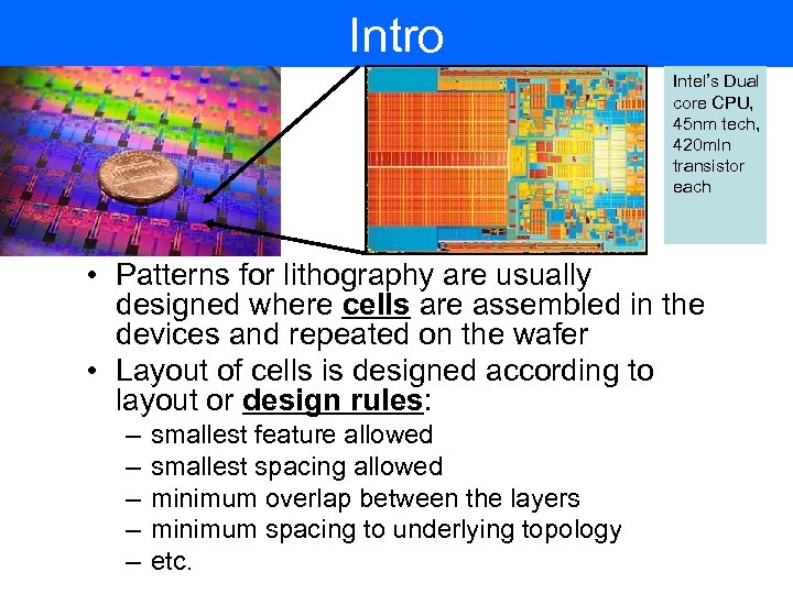 Intro Intel’s Dual core CPU, 45 nm tech, 420 mln transistor each • Patterns for lithography are usually designed where cells are assembled in the devices and repeated on the wafer • Layout of cells is designed according to layout or design rules: – – – smallest feature allowed smallest spacing allowed minimum overlap between the layers minimum spacing to underlying topology etc.
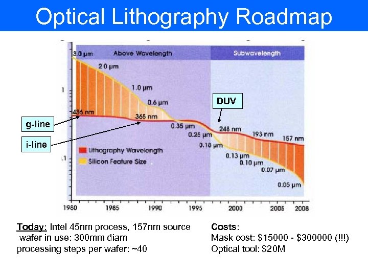 Optical Lithography Roadmap DUV g-line i-line Today: Intel 45 nm process, 157 nm source wafer in use: 300 mm diam processing steps per wafer: ~40 Costs: Mask cost: $15000 - $300000 (!!!) Optical tool: $20 M
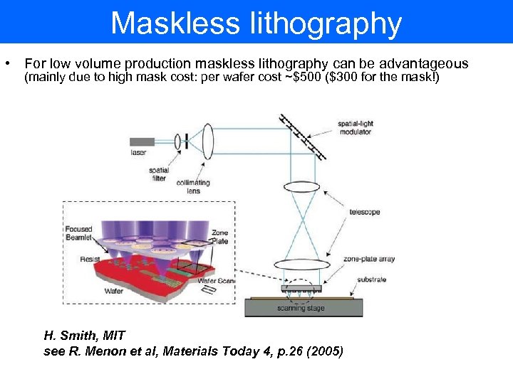
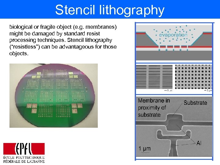
 Lecture plan • • • Diffraction and the resolution limits Modulation transfer function Light sources Contact/proximity printers: Mask Aligners Projection printers: Steppers Advanced techniques: – Phase-shift masks – Immersion lithography – Maskless lithography – Stencil lithography (“Resistless”)
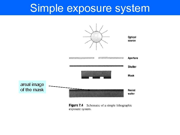 Simple exposure system areal image of the mask
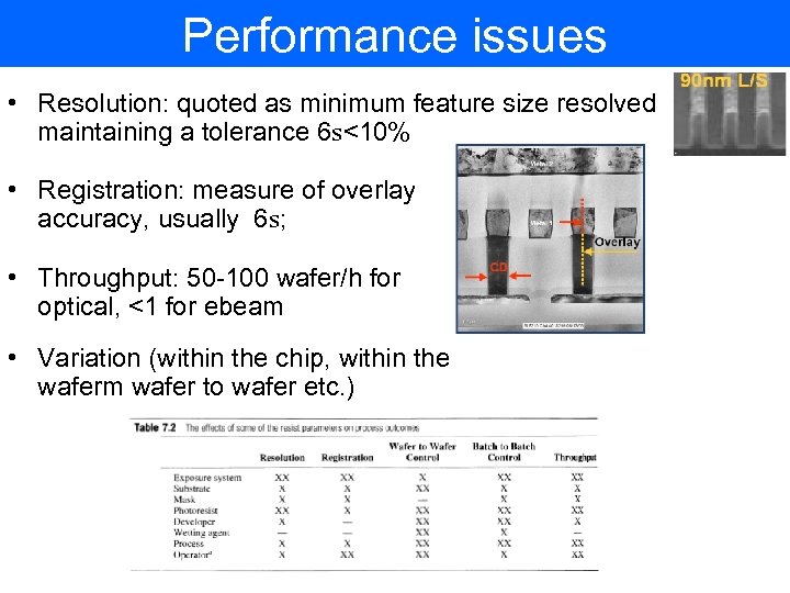 Performance issues • Resolution: quoted as minimum feature size resolved maintaining a tolerance 6 s<10% • Registration: measure of overlay accuracy, usually 6 s; • Throughput: 50 -100 wafer/h for optical, <1 for ebeam • Variation (within the chip, within the waferm wafer to wafer etc. )
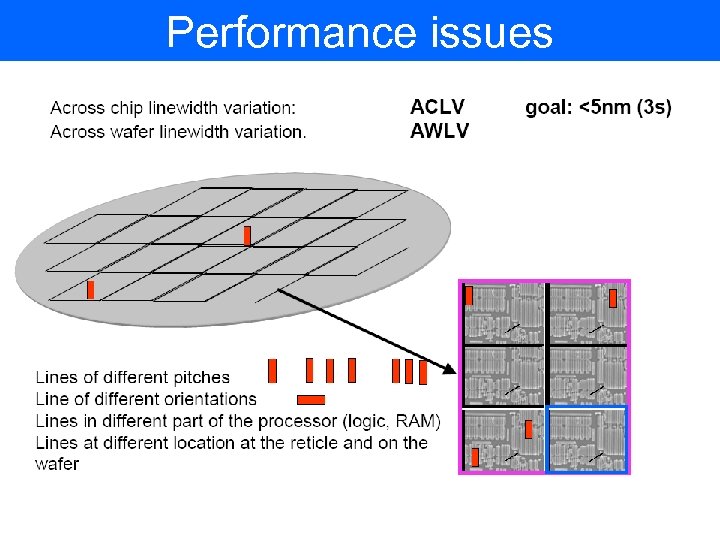 Performance issues
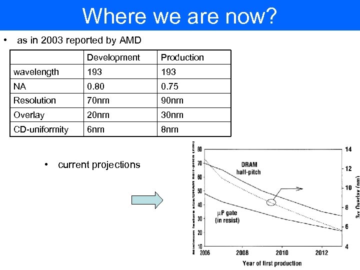 Where we are now? • as in 2003 reported by AMD Development Production wavelength 193 NA 0. 80 0. 75 Resolution 70 nm 90 nm Overlay 20 nm 30 nm CD-uniformity 6 nm 8 nm • current projections
 Requirements for the mask • Required properties: – high transparency at the exposure wavelength – small thermal expansion coefficient – flat highly polished surface • Photomask material: – fused silica – glass (soda-lime) for NUV applications; – opaque layer: usually chromium
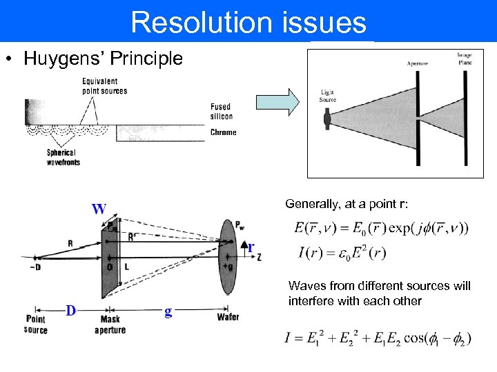 Resolution issues • Huygens’ Principle Generally, at a point r: Waves from different sources will interfere with each other
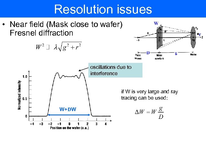 Resolution issues • Near field (Mask close to wafer) Fresnel diffraction oscillations due to interference if W is very large and ray tracing can be used: W+DW
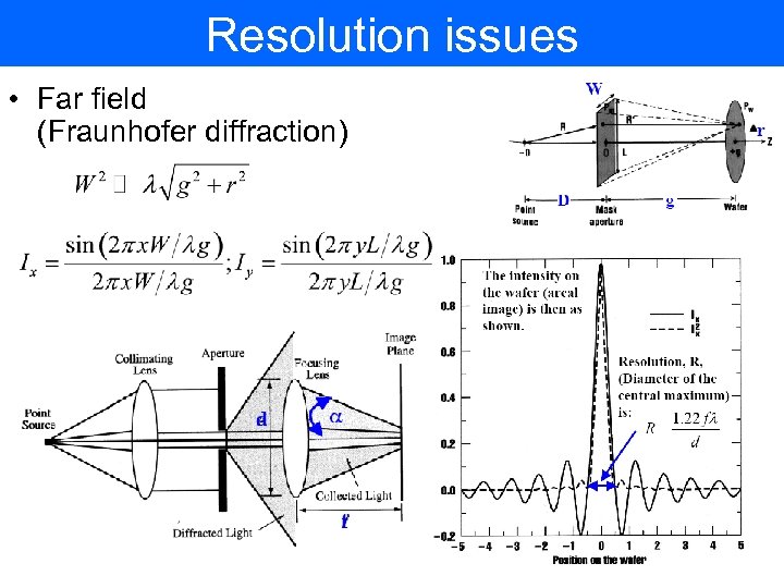 Resolution issues • Far field (Fraunhofer diffraction)
 Resolution issues • Other complications: – light source is not a point – imperfection of optical components – reflection, adsorption, phase shift on the mask – reflection on the wafer – etc…
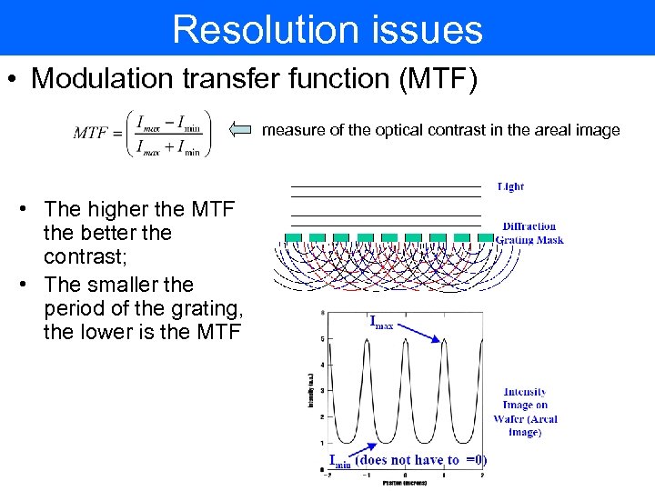 Resolution issues • Modulation transfer function (MTF) measure of the optical contrast in the areal image • The higher the MTF the better the contrast; • The smaller the period of the grating, the lower is the MTF
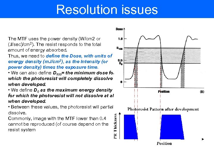 Resolution issues The MTF uses the power density (W/cm 2 or (J/sec)/cm 2). The resist responds to the total amount of energy absorbed. Thus, we need to define the Dose, with units of energy density (m. J/cm 2), as the Intensity (or power density) times the exposure time. • We can also define D 100= the minimum dose for which the photoresist will completely dissolve when developed. • We define D 0 as the maximum energy density for which the photoresist will not dissolve at all when developed. • Between these values, the photoresist will partially dissolve. Commonly, image with the MTF lower than 0. 4 cannot be reproduced (of course depend on the resist system
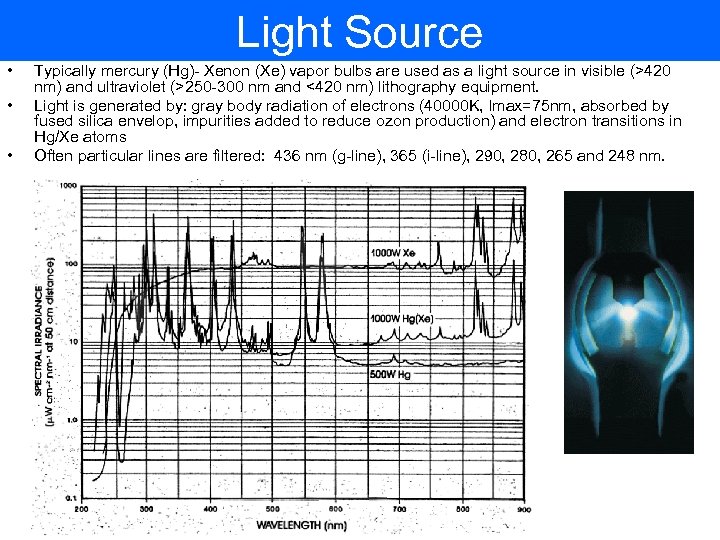 Light Source • • • Typically mercury (Hg)- Xenon (Xe) vapor bulbs are used as a light source in visible (>420 nm) and ultraviolet (>250 -300 nm and <420 nm) lithography equipment. Light is generated by: gray body radiation of electrons (40000 K, lmax=75 nm, absorbed by fused silica envelop, impurities added to reduce ozon production) and electron transitions in Hg/Xe atoms Often particular lines are filtered: 436 nm (g-line), 365 (i-line), 290, 280, 265 and 248 nm.
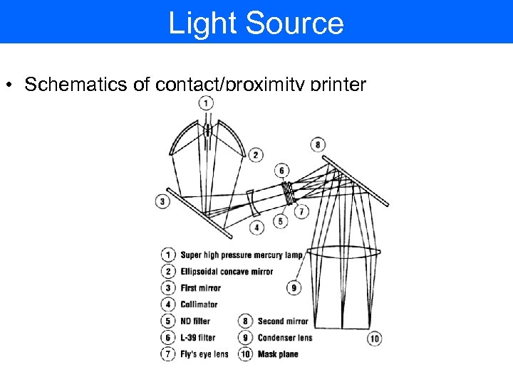 Light Source • Schematics of contact/proximity printer
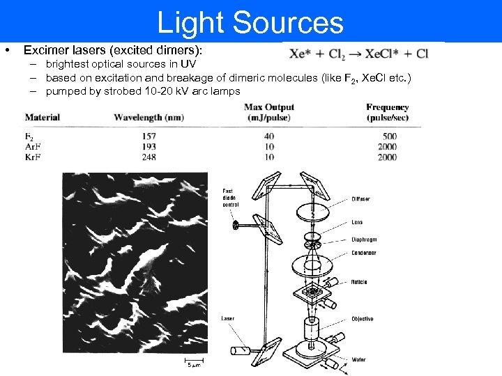 Light Sources • Excimer lasers (excited dimers): – brightest optical sources in UV – based on excitation and breakage of dimeric molecules (like F 2, Xe. Cl etc. ) – pumped by strobed 10 -20 k. V arc lamps
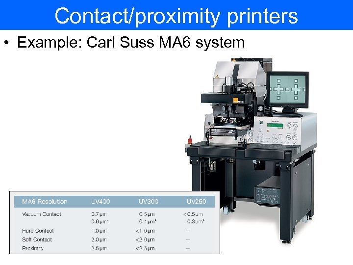 Contact/proximity printers • Example: Carl Suss MA 6 system
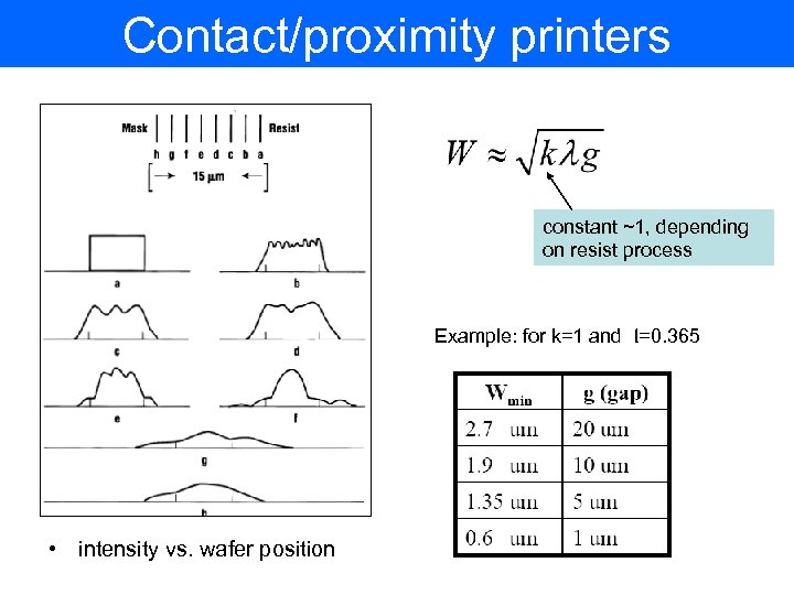 Contact/proximity printers constant ~1, depending on resist process Example: for k=1 and l=0. 365 • intensity vs. wafer position
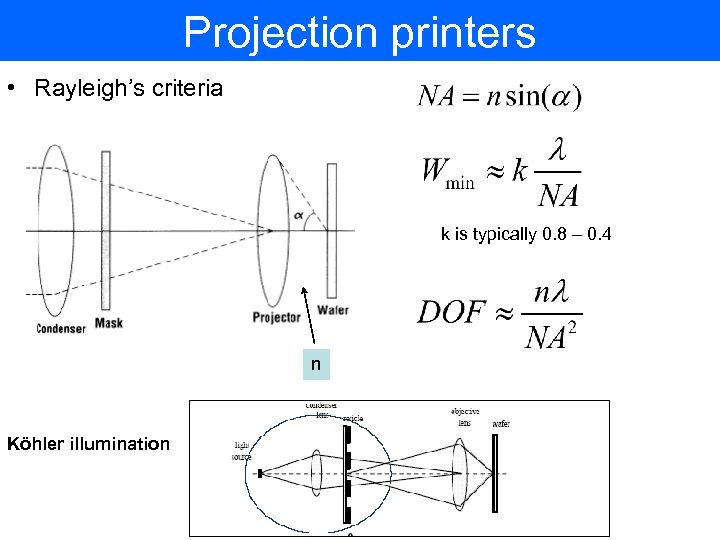 Projection printers • Rayleigh’s criteria k is typically 0. 8 – 0. 4 n Köhler illumination
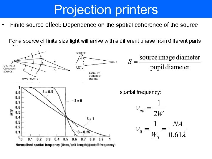 Projection printers • Finite source effect: Dependence on the spatial coherence of the source For a source of finite size light will arrive with a different phase from different parts of the source! spatial frequency:
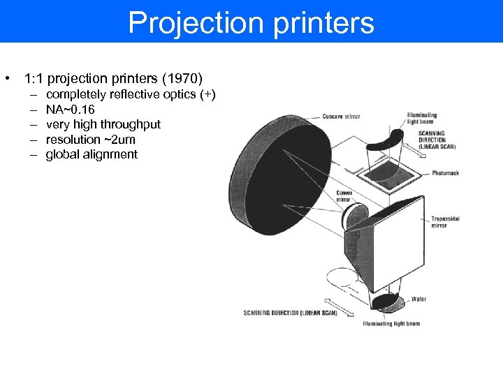 Projection printers • 1: 1 projection printers (1970) – – – completely reflective optics (+) NA~0. 16 very high throughput resolution ~2 um global alignment
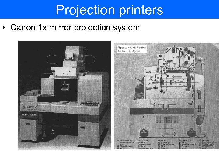 Projection printers • Canon 1 x mirror projection system
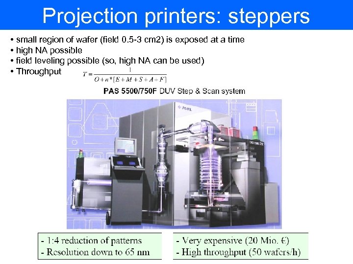 Projection printers: steppers • small region of wafer (field 0. 5 -3 cm 2) is exposed at a time • high NA possible • field leveling possible (so, high NA can be used) • Throughput
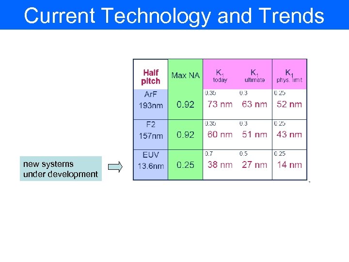
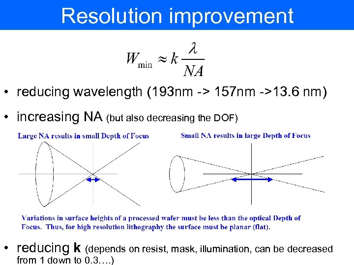 Resolution improvement • reducing wavelength (193 nm -> 157 nm ->13. 6 nm) • increasing NA (but also decreasing the DOF) • reducing k (depends on resist, mask, illumination, can be decreased from 1 down to 0. 3…. )
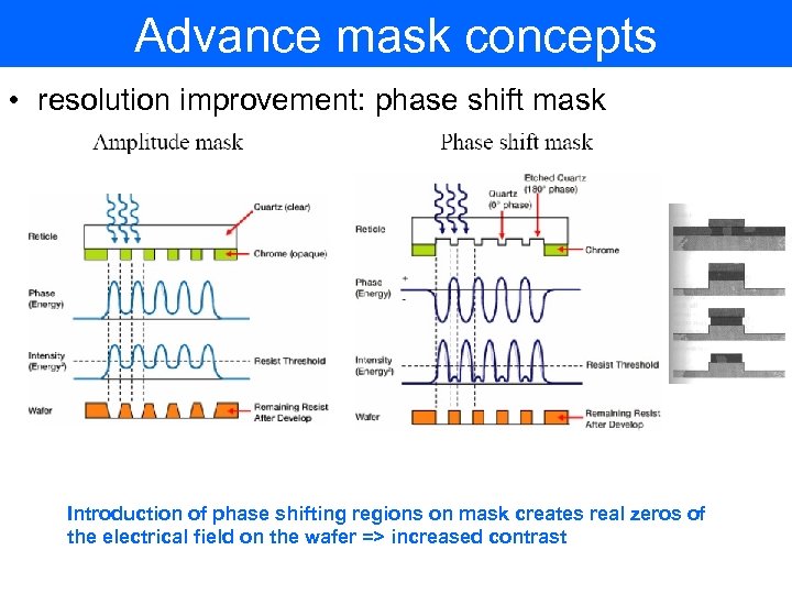 Advance mask concepts • resolution improvement: phase shift mask Introduction of phase shifting regions on mask creates real zeros of the electrical field on the wafer => increased contrast
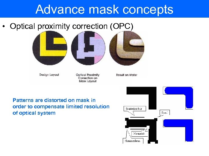 Advance mask concepts • Optical proximity correction (OPC) Patterns are distorted on mask in order to compensate limited resolution of optical system
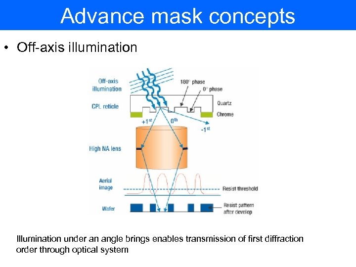 Advance mask concepts • Off-axis illumination Illumination under an angle brings enables transmission of first diffraction order through optical system
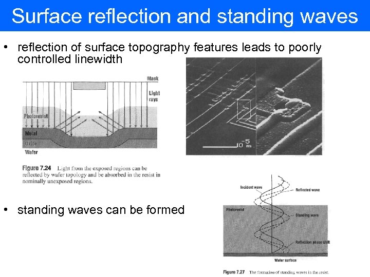 Surface reflection and standing waves • reflection of surface topography features leads to poorly controlled linewidth • standing waves can be formed
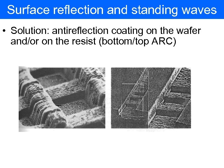 Surface reflection and standing waves • Solution: antireflection coating on the wafer and/or on the resist (bottom/top ARC)
 Immersion lithography
 Immersion lithography • improvement in resolution
 Immersion lithography • concept
 Immersion lithography roadmap without immersion with immersion
 Current Technology and Trends new systems under development
 Maskless lithography • For low volume production maskless lithography can be advantageous (mainly due to high mask cost: per wafer cost ~$500 ($300 for the mask!) H. Smith, MIT see R. Menon et al, Materials Today 4, p. 26 (2005)
 Fabrication of DNA arrays w. maskless lithography Fabrication of DNA array requires many lithographic steps (equal to number of bp), arrays are made on demand good candidate for maskless lithography S. Singh-Gasson et al, Nature Biotech. , 17, p. 974 (1999)
 Stencil lithography biological or fragile object (e. g. membranes) might be damaged by standard resist processing techniques. Stencil lithography (“resistless”) can be advantageous for those objects.
 Problems • Campbell 7. 4: In an effort to make a relatively inexpensive aligner, capable of producing very small features an optical source of a simple contact printer is replaced with Ar. F laser. – list 2 problems that the engineer is likely to encounter in trying to use this device, assume yield is unimportant – assume the resist constant 0. 8 for the process and the gap equal to resist thickness in hard contact. What is the minimum feature size for 1 um resist – How thin the resist should be made to achieve 0. 1 um resolution • Campbell 7. 8 A particular resist process is able to resolve features whose MTF≥ 0. 3. Using fig 7. 22 calculate the minimum feature size for an i-line aligner with NA=9. 4 and S=0. 5


