47ec6a52a5bfc348a1ef13e5894c4434.ppt
- Количество слайдов: 49
 Lecture 16 This lecture covers introductory aspects related to: - Sensors: Force, Pressure, Inertial, Chemical - Microoptics Dan O. Popa, EE 5349 Microsystems, Summer 2015
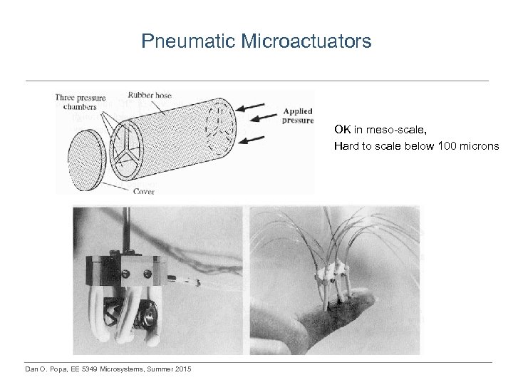 Pneumatic Microactuators OK in meso-scale, Hard to scale below 100 microns Dan O. Popa, EE 5349 Microsystems, Summer 2015
 Pneumatics Nozzles as Microgrippers • Automatic Assembly of a 1600 PIN Diode Array for a deep-space reflect-array antenna. • PIN Diode Example: M/A-COM MA 4 GP 907, with footprint of 380 x 700 m 2 • Assembly setup: – – Vaccum micro-gripper X, Y, Z, Theta (4 DOF) micropositioning system Epoxy stamping micro-tool Calibrated vision system Dan O. Popa, EE 5349 Microsystems, Summer 2015
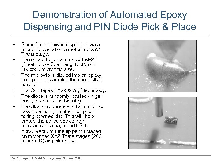 Demonstration of Automated Epoxy Dispensing and PIN Diode Pick & Place • • Silver-filled epoxy is dispensed via a micro-tip placed on a motorized XYZ Theta Stage. The micro-tip - a commercial SEST (Steel Epoxy Spamping Tool), with 260 x 580 micron tip size. The micro-tip is dipped into an epoxy pool prior to stamping the conductive traces. Tra-Con Bipax BA 2902 Ag filled epoxy. The diode is randomly located (in gelpack, or on a flat substrate). The diode is assumed to be in a facedown position (the electrical pads facing downwards). This will help protect the active device from mechanical damage and ESD. A #27 Vacuum tube tip pencil placed on motorized XYZ Theta stages (200 micron ID) as pick-up tool. Dan O. Popa, EE 5349 Microsystems, Summer 2015
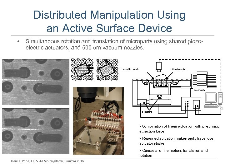 Distributed Manipulation Using an Active Surface Device • Simultaneous rotation and translation of microparts using shared piezoelectric actuators, and 500 um vacuum nozzles. movable nozzle fixed nozzle solenoids actuators § Combination of linear actuation with pneumatic attraction force § Repeated actuation makes parts travel over actuator stroke § Coarse and fine motion, translation and rotation Dan O. Popa, EE 5349 Microsystems, Summer 2015
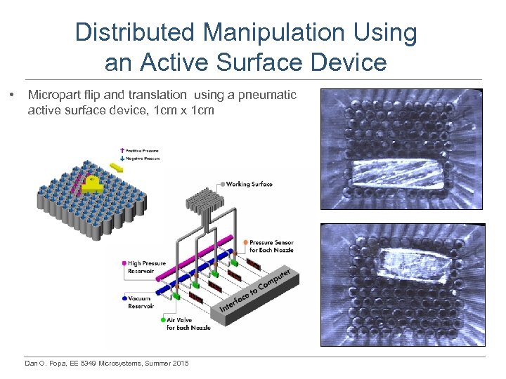 Distributed Manipulation Using an Active Surface Device • Micropart flip and translation using a pneumatic active surface device, 1 cm x 1 cm Dan O. Popa, EE 5349 Microsystems, Summer 2015
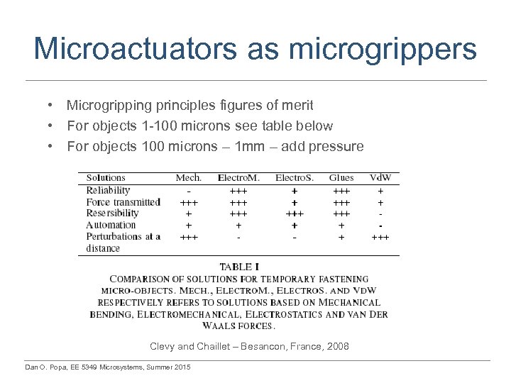 Microactuators as microgrippers • Microgripping principles figures of merit • For objects 1 -100 microns see table below • For objects 100 microns – 1 mm – add pressure Clevy and Chaillet – Besancon, France, 2008 Dan O. Popa, EE 5349 Microsystems, Summer 2015
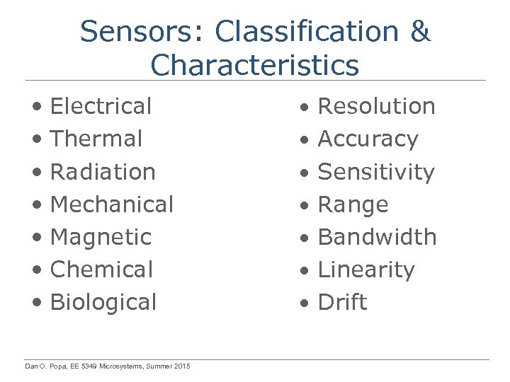 Sensors: Classification & Characteristics • Electrical • Thermal • Radiation • Mechanical • Magnetic • Chemical • Biological Dan O. Popa, EE 5349 Microsystems, Summer 2015 • • Resolution Accuracy Sensitivity Range Bandwidth Linearity Drift
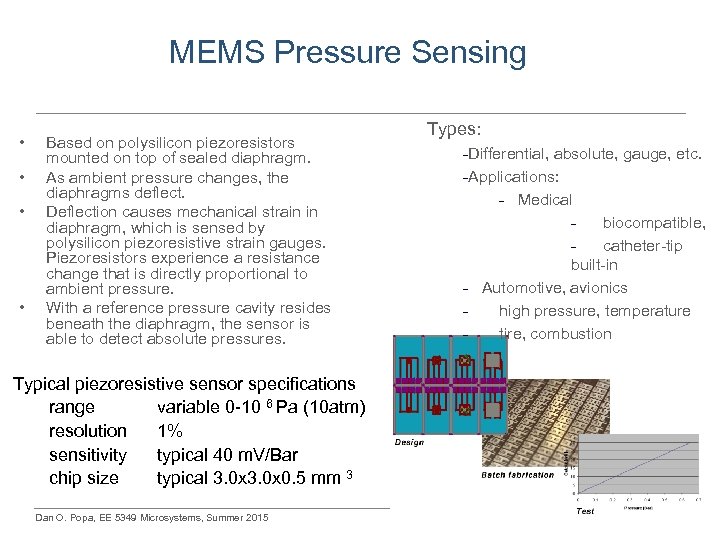 MEMS Pressure Sensing • • Based on polysilicon piezoresistors mounted on top of sealed diaphragm. As ambient pressure changes, the diaphragms deflect. Deflection causes mechanical strain in diaphragm, which is sensed by polysilicon piezoresistive strain gauges. Piezoresistors experience a resistance change that is directly proportional to ambient pressure. With a reference pressure cavity resides beneath the diaphragm, the sensor is able to detect absolute pressures. Typical piezoresistive sensor specifications range variable 0 -10 6 Pa (10 atm) resolution 1% sensitivity typical 40 m. V/Bar chip size typical 3. 0 x 0. 5 mm 3 Dan O. Popa, EE 5349 Microsystems, Summer 2015 Types: -Differential, absolute, gauge, etc. -Applications: - Medical biocompatible, catheter-tip built-in - Automotive, avionics high pressure, temperature tire, combustion
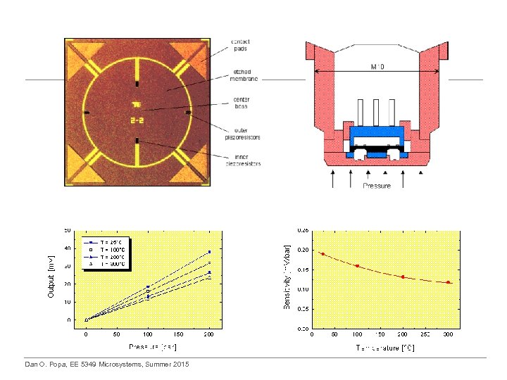
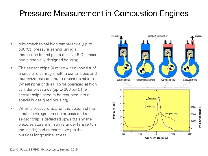 Pressure Measurement in Combustion Engines • Micromechanical high temperature (up to 500°C) pressure sensor using a membrane based piezoresistive Si. C sensor and a specially designed housing • The sensor chips (4 mm x 4 mm) consist of a circular diaphragm with a center boss and four piezoresistors that are connected in a Wheatstone bridge). To be operated at high cylinder pressures (up to 200 bar), the sensor chips need to be mounted into a specially designed housing). • When a pressure acts on the bottom of the steel diaphragm the center boss of the sensor chip is deflected upwards and the piezoresistors are in pairs under tensile (on the inside) and compressive (on the outside) longitudinal stress. Dan O. Popa, EE 5349 Microsystems, Summer 2015
 Dan O. Popa, EE 5349 Microsystems, Summer 2015
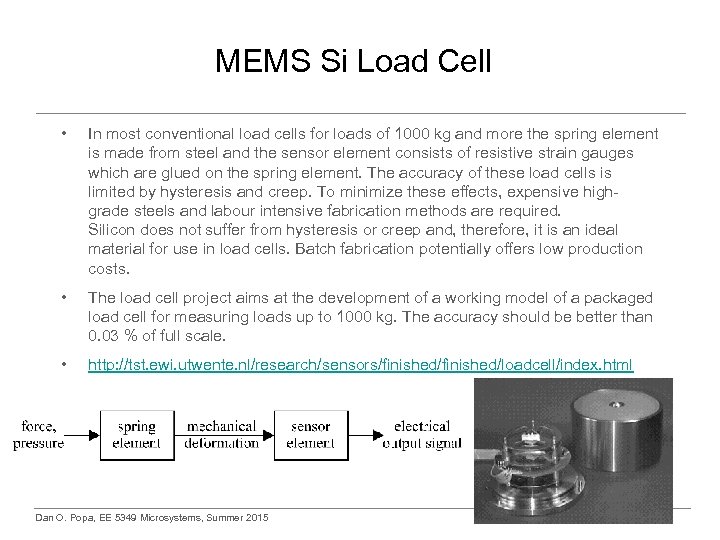 MEMS Si Load Cell • In most conventional load cells for loads of 1000 kg and more the spring element is made from steel and the sensor element consists of resistive strain gauges which are glued on the spring element. The accuracy of these load cells is limited by hysteresis and creep. To minimize these effects, expensive highgrade steels and labour intensive fabrication methods are required. Silicon does not suffer from hysteresis or creep and, therefore, it is an ideal material for use in load cells. Batch fabrication potentially offers low production costs. • The load cell project aims at the development of a working model of a packaged load cell for measuring loads up to 1000 kg. The accuracy should be better than 0. 03 % of full scale. • http: //tst. ewi. utwente. nl/research/sensors/finished/loadcell/index. html Dan O. Popa, EE 5349 Microsystems, Summer 2015
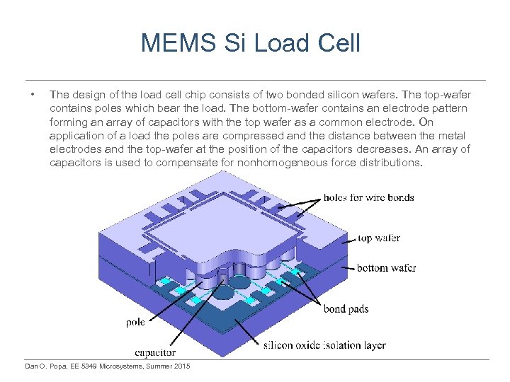 MEMS Si Load Cell • The design of the load cell chip consists of two bonded silicon wafers. The top-wafer contains poles which bear the load. The bottom-wafer contains an electrode pattern forming an array of capacitors with the top wafer as a common electrode. On application of a load the poles are compressed and the distance between the metal electrodes and the top-wafer at the position of the capacitors decreases. An array of capacitors is used to compensate for nonhomogeneous force distributions. Dan O. Popa, EE 5349 Microsystems, Summer 2015
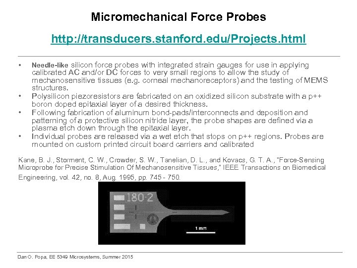 Micromechanical Force Probes http: //transducers. stanford. edu/Projects. html • • Needle-like silicon force probes with integrated strain gauges for use in applying calibrated AC and/or DC forces to very small regions to allow the study of mechanosensitive tissues (e. g. corneal mechanoreceptors) and the testing of MEMS structures. Polysilicon piezoresistors are fabricated on an oxidized silicon substrate with a p++ boron doped epitaxial layer of a desired thickness. Following fabrication of aluminum bond-pads/interconnects and deposition and patterning of a protective silicon nitride layer, the probe shapes are defined via a plasma etch down through the epitaxial layer. Individual probes are released via a wet etch that stops on p++ regions. Probes are mounted on custom printed circuit board carriers and calibrated Kane, B. J. , Storment, C. W. , Crowder, S. W. , Tanelian, D. L. , and Kovacs, G. T. A. , “Force-Sensing Microprobe for Precise Stimulation Of Mechanosensitive Tissues, ” IEEE Transactions on Biomedical Engineering, vol. 42, no. 8, Aug. 1995, pp. 745 - 750. Dan O. Popa, EE 5349 Microsystems, Summer 2015
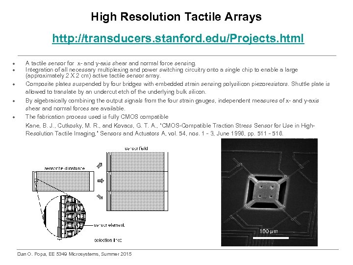 High Resolution Tactile Arrays http: //transducers. stanford. edu/Projects. html · · · A tactile sensor for x- and y-axis shear and normal force sensing. Integration of all necessary multiplexing and power switching circuitry onto a single chip to enable a large (approximately 2 X 2 cm) active tactile sensor array. Composite plates suspended by four bridges with embedded strain sensing polysilicon piezoresistors. Shuttle plate is allowed to translate by an undercut etch of the underlying bulk silicon. By algebraically combining the output signals from the four strain gauges, independent measures of x- and y-axis shear and normal forces are available. The fabrication process used is fully CMOS compatible Kane, B. J. , Cutkosky, M. R. , and Kovacs, G. T. A. , “CMOS-Compatible Traction Stress Sensor for Use in High. Resolution Tactile Imaging, ” Sensors and Actuators A, vol. 54, nos. 1 - 3, June 1996, pp. 511 - 516. Dan O. Popa, EE 5349 Microsystems, Summer 2015
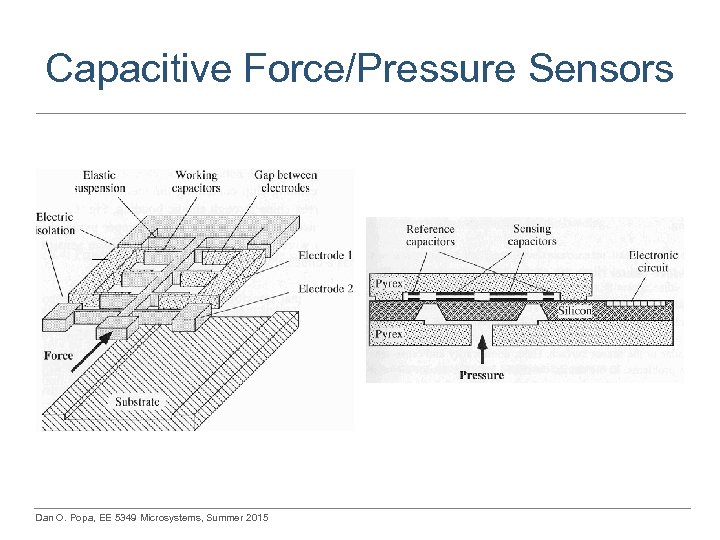 Capacitive Force/Pressure Sensors Dan O. Popa, EE 5349 Microsystems, Summer 2015
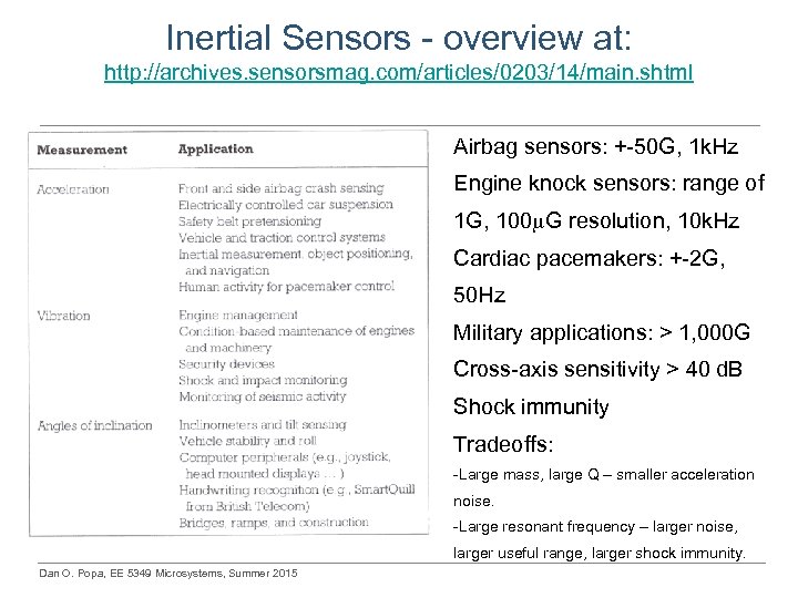 Inertial Sensors - overview at: http: //archives. sensorsmag. com/articles/0203/14/main. shtml Airbag sensors: +-50 G, 1 k. Hz Engine knock sensors: range of 1 G, 100 G resolution, 10 k. Hz Cardiac pacemakers: +-2 G, 50 Hz Military applications: > 1, 000 G Cross-axis sensitivity > 40 d. B Shock immunity Tradeoffs: -Large mass, large Q – smaller acceleration noise. -Large resonant frequency – larger noise, larger useful range, larger shock immunity. Dan O. Popa, EE 5349 Microsystems, Summer 2015
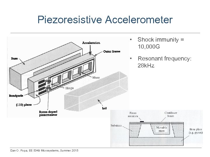 Piezoresistive Accelerometer • Shock immunity = 10, 000 G • Resonant frequency: 28 k. Hz Dan O. Popa, EE 5349 Microsystems, Summer 2015
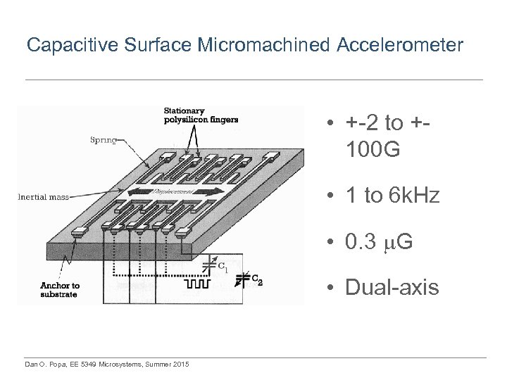 Capacitive Surface Micromachined Accelerometer • +-2 to +100 G • 1 to 6 k. Hz • 0. 3 G • Dual-axis Dan O. Popa, EE 5349 Microsystems, Summer 2015
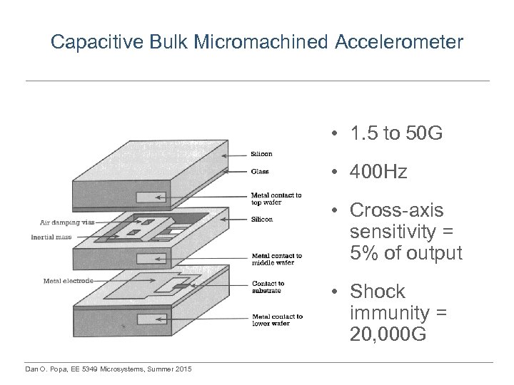 Capacitive Bulk Micromachined Accelerometer • 1. 5 to 50 G • 400 Hz • Cross-axis sensitivity = 5% of output • Shock immunity = 20, 000 G Dan O. Popa, EE 5349 Microsystems, Summer 2015
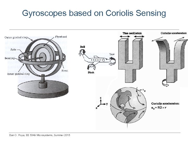 Gyroscopes based on Coriolis Sensing Dan O. Popa, EE 5349 Microsystems, Summer 2015
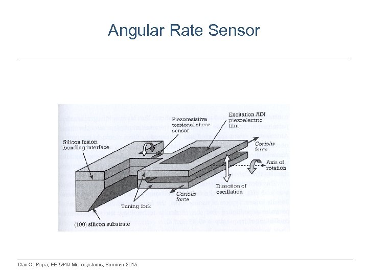 Angular Rate Sensor Dan O. Popa, EE 5349 Microsystems, Summer 2015
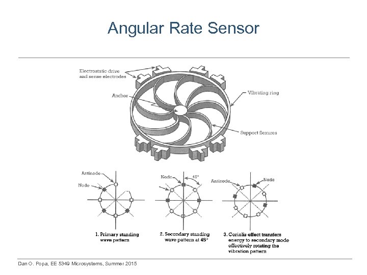 Angular Rate Sensor Dan O. Popa, EE 5349 Microsystems, Summer 2015
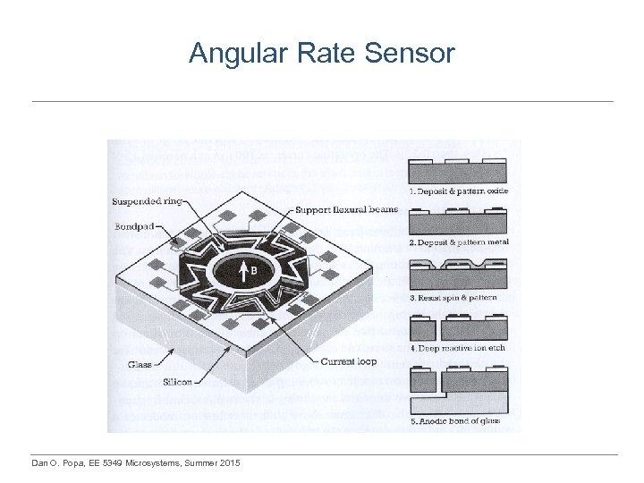 Angular Rate Sensor Dan O. Popa, EE 5349 Microsystems, Summer 2015
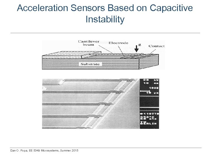 Acceleration Sensors Based on Capacitive Instability Dan O. Popa, EE 5349 Microsystems, Summer 2015
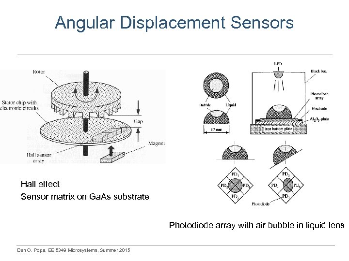 Angular Displacement Sensors Hall effect Sensor matrix on Ga. As substrate Photodiode array with air bubble in liquid lens Dan O. Popa, EE 5349 Microsystems, Summer 2015
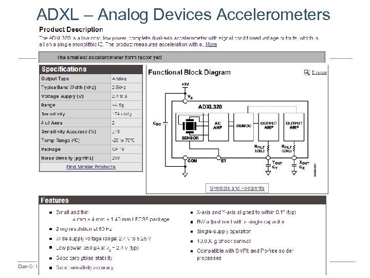 ADXL – Analog Devices Accelerometers Dan O. Popa, EE 5349 Microsystems, Summer 2015
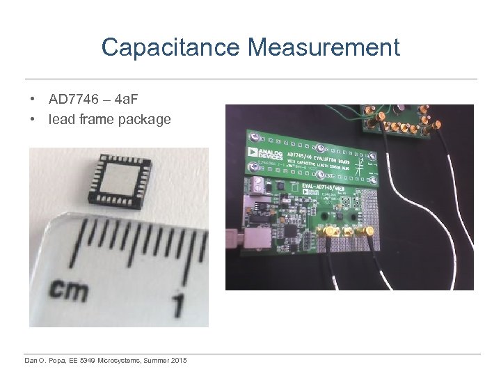 Capacitance Measurement • AD 7746 – 4 a. F • lead frame package Dan O. Popa, EE 5349 Microsystems, Summer 2015
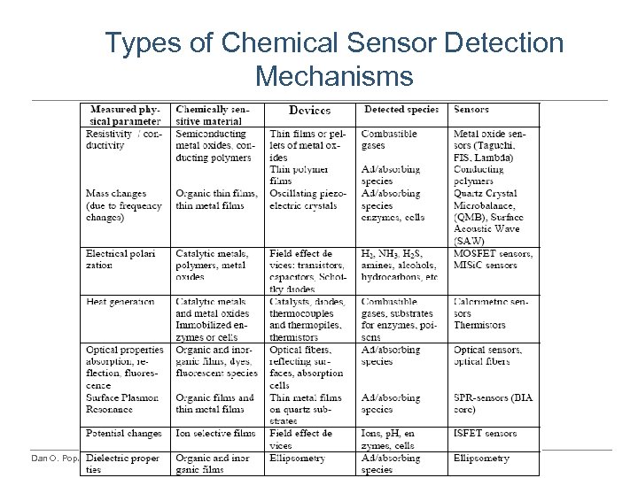 Types of Chemical Sensor Detection Mechanisms Dan O. Popa, EE 5349 Microsystems, Summer 2015
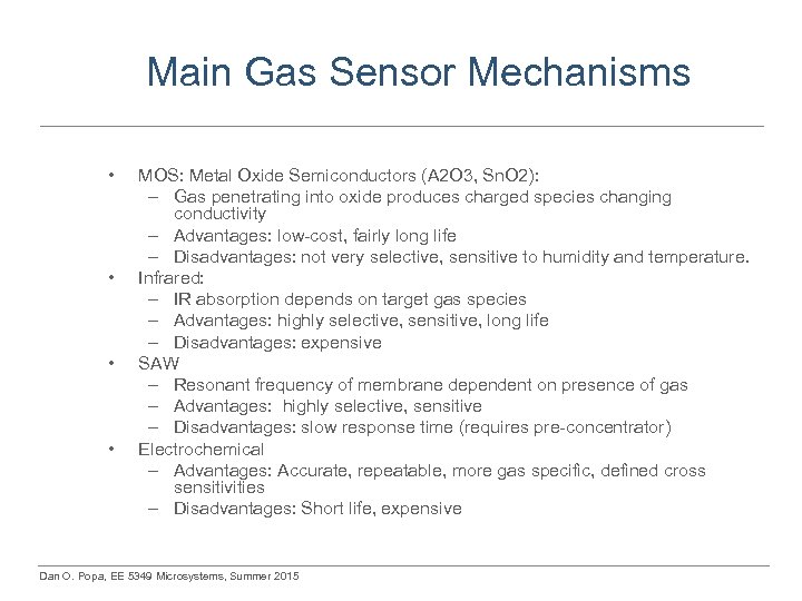 Main Gas Sensor Mechanisms • • MOS: Metal Oxide Semiconductors (A 2 O 3, Sn. O 2): – Gas penetrating into oxide produces charged species changing conductivity – Advantages: low-cost, fairly long life – Disadvantages: not very selective, sensitive to humidity and temperature. Infrared: – IR absorption depends on target gas species – Advantages: highly selective, sensitive, long life – Disadvantages: expensive SAW – Resonant frequency of membrane dependent on presence of gas – Advantages: highly selective, sensitive – Disadvantages: slow response time (requires pre-concentrator) Electrochemical – Advantages: Accurate, repeatable, more gas specific, defined cross sensitivities – Disadvantages: Short life, expensive Dan O. Popa, EE 5349 Microsystems, Summer 2015
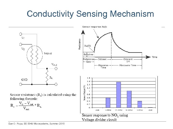 Conductivity Sensing Mechanism Sensor response to NO 2 using Voltage divider circuit Dan O. Popa, EE 5349 Microsystems, Summer 2015
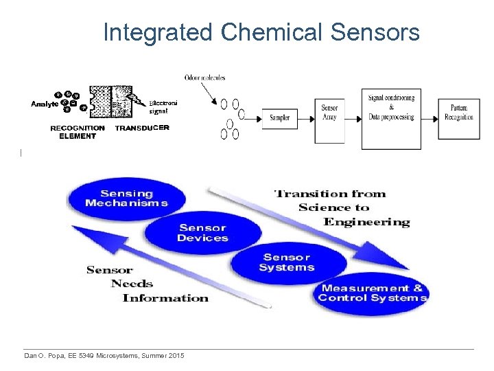 Integrated Chemical Sensors Dan O. Popa, EE 5349 Microsystems, Summer 2015
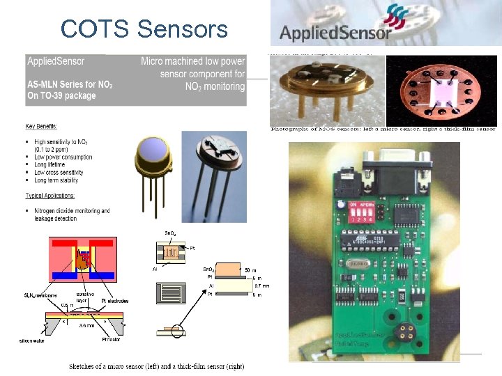 COTS Sensors Dan O. Popa, EE 5349 Microsystems, Summer 2015
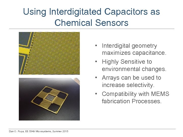 Using Interdigitated Capacitors as Chemical Sensors • Interdigital geometry maximizes capacitance. • Highly Sensitive to environmental changes. • Arrays can be used to increase selectivity. • Compatibility with MEMS fabrication Processes. Dan O. Popa, EE 5349 Microsystems, Summer 2015
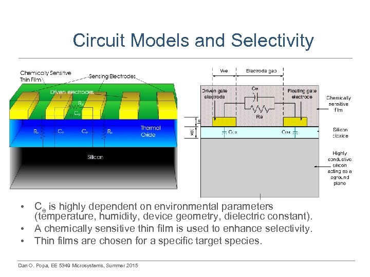 Circuit Models and Selectivity • • • Ce is highly dependent on environmental parameters (temperature, humidity, device geometry, dielectric constant). A chemically sensitive thin film is used to enhance selectivity. Thin films are chosen for a specific target species. Dan O. Popa, EE 5349 Microsystems, Summer 2015
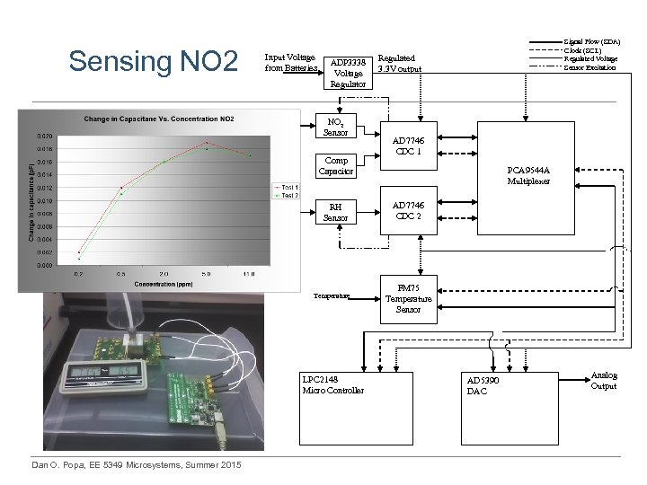 Sensing NO 2 Input Voltage from Batteries NO 2 ADP 3338 Voltage Regulator NO 2 Sensor Comp Capacitor RH RH Sensor Temperature LPC 2148 Micro Controller Dan O. Popa, EE 5349 Microsystems, Summer 2015 Signal Flow (SDA) Clock (SCL) Regulated Voltage Sensor Excitation Regulated 3. 3 V output AD 7746 CDC 1 PCA 9544 A Multiplexer AD 7746 CDC 2 FM 75 Temperature Sensor AD 5390 DAC Analog Output
 Microphotonics (Microoptics) l Photonics: blend of optics and electronics. l Photonic materials/devices/systems. l Brief history: • 1870 - John Tyndall’s experiment (water jets as light transmission medium). • 1880 - Alexander Graham Bell’s unguided light carrying speech system. • 1950 – O’Brien & Kapany build first image carrying fibers, used today in fiberscopes. • 1957– 1960 – Gould/Townes/Maiman develop first lasers. • 1966 -1970 Maurer, Keck, and Schultz at Corning invent fiberoptics with low loss, 20 db/km • 1970’s and 1980’s – fiber optic infrastructure built for telephony, improvements in fiber glass manufacturing (losses 0. 2 db/km). • 1990’s and 2000’s – Gigabit ethernet infrastructure based on fiber optics. Dan O. Popa, EE 5349 Microsystems, Summer 2015
 Photonic Materials • • Semiconductor Materials • • • Used for light generation, detection, modulation, fabrication of monolithic devices III-V semiconductors (Ga. As) used in. 65 -1. 55 μm lasers. II-VI, III-N used for visible and UV lasers. Ferroelectric Materials • Used in spatial light modulation, light beam amplification, optical storage. Nonlinear Optical Materials • Crystalline and Polymeric Glass (Silica) • Used for fiber, lenses, collimators. Dan O. Popa, EE 5349 Microsystems, Summer 2015
 Photonic Devices • • • Semiconductor diode lasers (LED) • Based on a semiconductor diode junction, electron-hole recombination produces photons. Photodetectors • • Inverse of LED’s. PIN, MSM, Avalanche. Solid-State Lasers • • Consists of an active medium with energy levels selectively populated. A pump to produce population inversion. A resonant EM cavity for feedback. Built with glasses doped with rare-earth dopants: Erbium, Yttrium, Thulium, Holmium, Neodymium. Dan O. Popa, EE 5349 Microsystems, Summer 2015
 Photonic Devices • Optical modulators • • Used to change the phase, polarization and amplitude of light. Modulation mechanism: Electro-optic, Acousto-optic, Magneto-optic, Micromechanical, Thermal. Optical Fibers • • • Pioneered by Corning, Inc. Made by removing impurities from glass, and doping it. Advantages of fiber over copper wire: wide bandwidth, low loss, EMI immunity, light weight, small size. Mirrors, Lenses (micro and macro) • Metal, Glass, other dielectric coatings Dan O. Popa, EE 5349 Microsystems, Summer 2015
 Not all detectors of radiation are photonic: example - IR Detectors • Thermal – Thermopile: thermal energy generates electrical energy, series or parallels of thermocouples (Seebeck effect) – Microbolometer: IR radiation changes resistance, vanadium oxide, amorphous silicon – Pyroelectric: IR changes crystal temperature, spontaneous polarization, then it generate electrical charges (Li. Ta. O 3: Litium Tantalate, DLa. TGS: Deuterated L-Alanyne Triglycine Sulphate, TGS, DTGS) • Photonic: high detectivity and fast – Photoconductive, Photovoltaic – Hg. Cd. Te (MCT), Pb. Se Dan O. Popa, EE 5349 Microsystems, Summer 2015
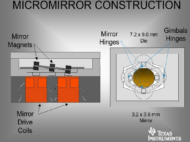
 MOEMS devices • • Micro-opto-electro-mechanical systems (MOEMS). Some of the devices could be fabricated using IC technology. Other MOEMS devices require different fabrication and assembly technologies. Can be integrated with electronics on the same chip. Must be scalable to a large number of devices. Must be small and cheap to manufacture. Some require hermetic packaging. Commercial examples of MOEMS: • • • TI Digital Micromirror Array (DLP™) AT&T Microactuated Switch Mirror. Lucent 2 N Micromirror Switch. Dan O. Popa, EE 5349 Microsystems, Summer 2015
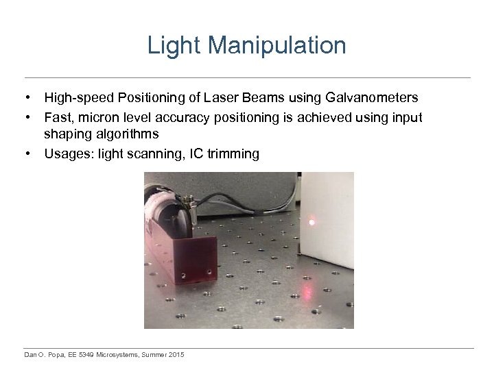 Light Manipulation • High-speed Positioning of Laser Beams using Galvanometers • Fast, micron level accuracy positioning is achieved using input shaping algorithms • Usages: light scanning, IC trimming Dan O. Popa, EE 5349 Microsystems, Summer 2015
 Dan O. Popa, EE 5349 Microsystems, Summer 2015
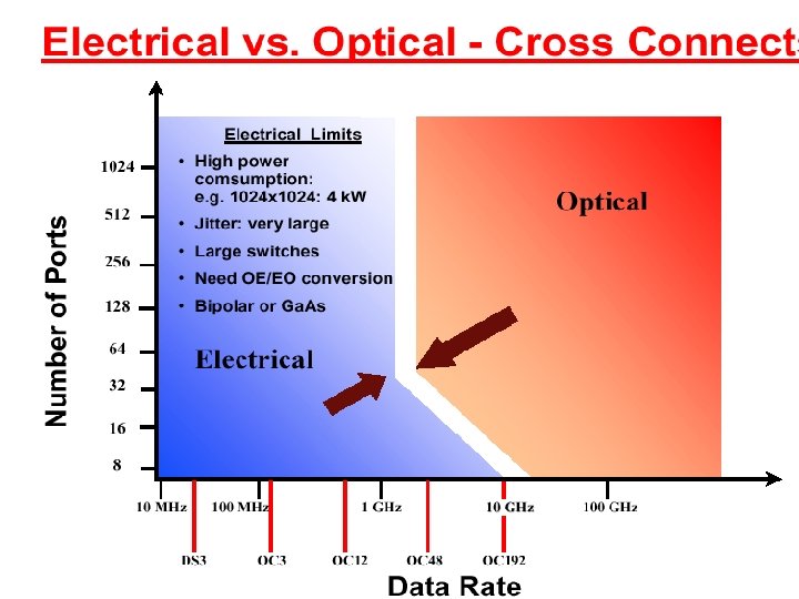 Dan O. Popa, EE 5349 Microsystems, Summer 2015
 Challenges in MOEMS • Micro-mirrors are easy to manufacture using IC technology. What about integrating micro-lenses, micro-arrays of fiber, etc? • New micro-technology dealing with glass must be developed, including micro-grasping, micro-positioning and bonding. • Cost effective/ large quantity automated assembly systems for MOEMS are not currently available. • • • The management of large number of fibers in MOEMS devices. Scalable designs of MOEMS. Fluxless attachment/hermetic packaging for long term reliability. Dan O. Popa, EE 5349 Microsystems, Summer 2015
 Introduction to fiber-optics • • • Fiber components: core, cladding, buffer, jacket. Materials used: glass, plastic (PFO). Multimode/singlemode operation – variable diameter: • • 62. 5 µm core, LED, used in LAN 9 µm core, laser, used in CATV, telephony. Wavelength: • • • IR 850 nm-1300 nm(Multimode) IR 1300 nm-1550 nm(Singlemode) Visible & IR 650 nm-850 nm Wave source: LED, laser (VCSEL, vertical cavity surface emitting laser) Dan O. Popa, EE 5349 Microsystems, Summer 2015
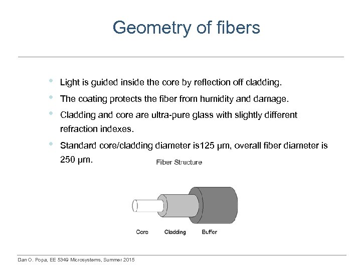 Geometry of fibers • • • Light is guided inside the core by reflection off cladding. The coating protects the fiber from humidity and damage. Cladding and core are ultra-pure glass with slightly different refraction indexes. • Standard core/cladding diameter is 125 µm, overall fiber diameter is 250 µm. Dan O. Popa, EE 5349 Microsystems, Summer 2015
 Readings for Week 16 • Fatikow Text, Chapter 6 • Madou Text, Chapter 8 Dan O. Popa, EE 5349 Microsystems, Summer 2015


