34075a5d62600c04f89f29ab5c01e545.ppt
- Количество слайдов: 27
 Lecture 16 alt Analog Circuit Test (Alternative to Lectures 17, 18, 19 and 30) • Analog circuits • Analog circuit test methods • Specification-based testing • Direct measurement • DSP-based testing • Fault model based testing • IEEE 1149. 4 analog test bus standard • Summary • References Copyright 2005, Agrawal & Bushnell VLSI Test: Lecture 16 alt 1
 Analog Circuits § § § § § Operational amplifier (analog) Programmable gain amplifier (mixed-signal) Filters, active and passive (analog) Comparator (mixed-signal) Voltage regulator (analog or mixed-signal) Analog mixer (analog) Analog switches (analog) Analog to digital converter (mixed-signal) Digital to analog converter (mixed-signal) Phase locked loop (PLL) (mixed-signal) Copyright 2005, Agrawal & Bushnell VLSI Test: Lecture 16 alt 2
 Test Parameters § DC § AC § Continuity § Leakage current § Reference voltage § Impedance § Gain § Power supply – sensitivity, common mode rejection § Gain – frequency and phase response § Distortion – harmonic, intermodulation, nonlinearity, § crosstalk Noise – SNR, noise figure Copyright 2005, Agrawal & Bushnell VLSI Test: Lecture 16 alt 3
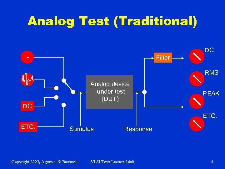 Analog Test (Traditional) DC ~ Filter RMS Analog device under test (DUT) PEAK DC ETC. Stimulus Copyright 2005, Agrawal & Bushnell Response VLSI Test: Lecture 16 alt 4
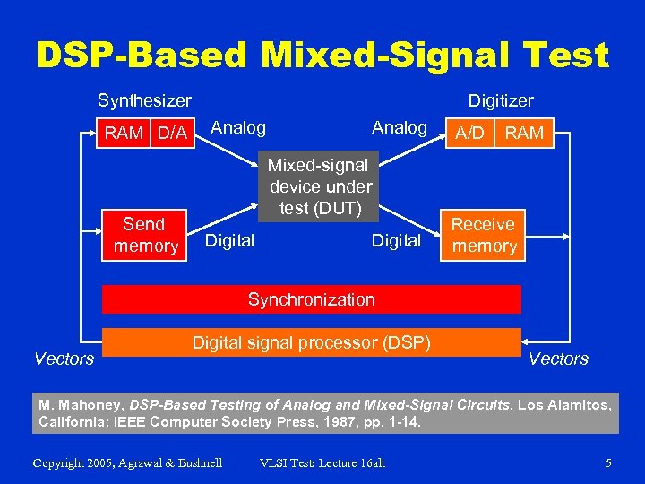 DSP-Based Mixed-Signal Test Synthesizer RAM D/A Send memory Digitizer Analog A/D Digital Receive memory Mixed-signal device under test (DUT) Digital RAM Synchronization Vectors Digital signal processor (DSP) Vectors M. Mahoney, DSP-Based Testing of Analog and Mixed-Signal Circuits, Los Alamitos, California: IEEE Computer Society Press, 1987, pp. 1 -14. Copyright 2005, Agrawal & Bushnell VLSI Test: Lecture 16 alt 5
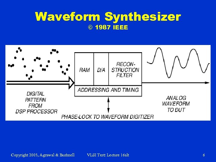 Waveform Synthesizer © 1987 IEEE Copyright 2005, Agrawal & Bushnell VLSI Test: Lecture 16 alt 6
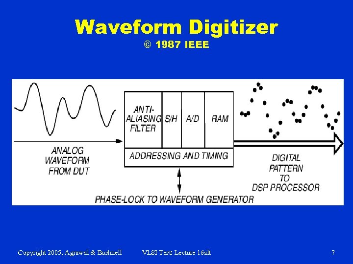 Waveform Digitizer © 1987 IEEE Copyright 2005, Agrawal & Bushnell VLSI Test: Lecture 16 alt 7
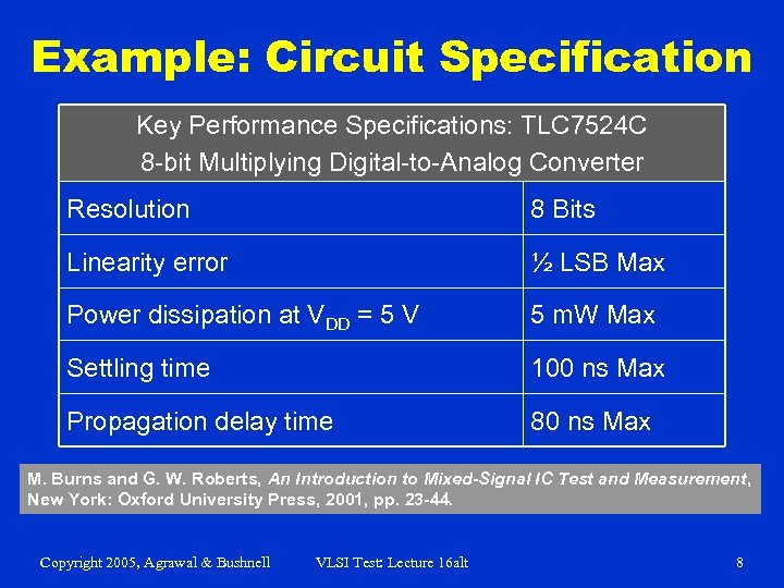 Example: Circuit Specification Key Performance Specifications: TLC 7524 C 8 -bit Multiplying Digital-to-Analog Converter Resolution 8 Bits Linearity error ½ LSB Max Power dissipation at VDD = 5 V 5 m. W Max Settling time 100 ns Max Propagation delay time 80 ns Max M. Burns and G. W. Roberts, An Introduction to Mixed-Signal IC Test and Measurement, New York: Oxford University Press, 2001, pp. 23 -44. Copyright 2005, Agrawal & Bushnell VLSI Test: Lecture 16 alt 8
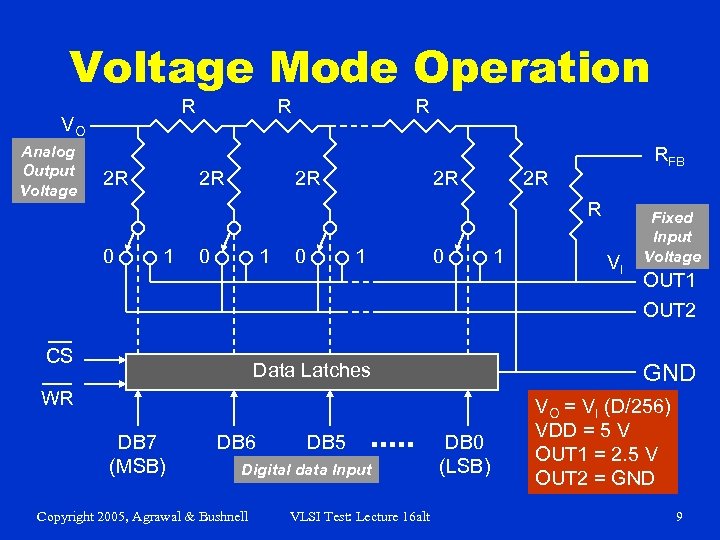 Voltage Mode Operation R VO Analog Output Voltage 2 R R 2 R 2 R RFB 2 R R 0 1 CS 0 1 0 Data Latches DB 6 DB 5 Digital data Input Copyright 2005, Agrawal & Bushnell VLSI Test: Lecture 16 alt VI OUT 1 OUT 2 GND WR DB 7 (MSB) 1 Fixed Input Voltage DB 0 (LSB) VO = VI (D/256) VDD = 5 V OUT 1 = 2. 5 V OUT 2 = GND 9
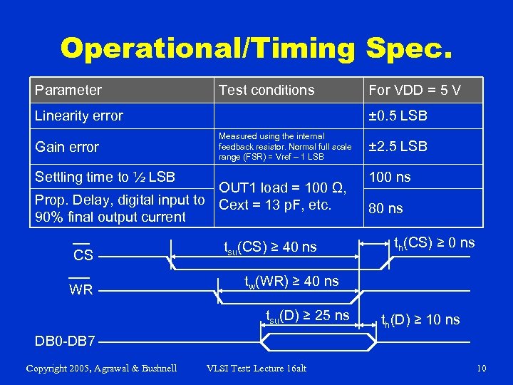 Operational/Timing Spec. Parameter Test conditions ± 0. 5 LSB Linearity error Gain error Measured using the internal feedback resistor. Normal full scale range (FSR) = Vref – 1 LSB Settling time to ½ LSB OUT 1 load = 100 Ω, Prop. Delay, digital input to Cext = 13 p. F, etc. 90% final output current CS WR For VDD = 5 V tsu(CS) ≥ 40 ns ± 2. 5 LSB 100 ns 80 ns th(CS) ≥ 0 ns tw(WR) ≥ 40 ns tsu(D) ≥ 25 ns th(D) ≥ 10 ns DB 0 -DB 7 Copyright 2005, Agrawal & Bushnell VLSI Test: Lecture 16 alt 10
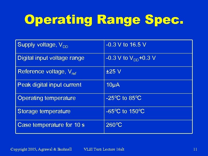 Operating Range Spec. Supply voltage, VDD -0. 3 V to 16. 5 V Digital input voltage range -0. 3 V to VDD+0. 3 V Reference voltage, Vref ± 25 V Peak digital input current 10μA Operating temperature -25ºC to 85ºC Storage temperature -65ºC to 150ºC Case temperature for 10 s 260ºC Copyright 2005, Agrawal & Bushnell VLSI Test: Lecture 16 alt 11
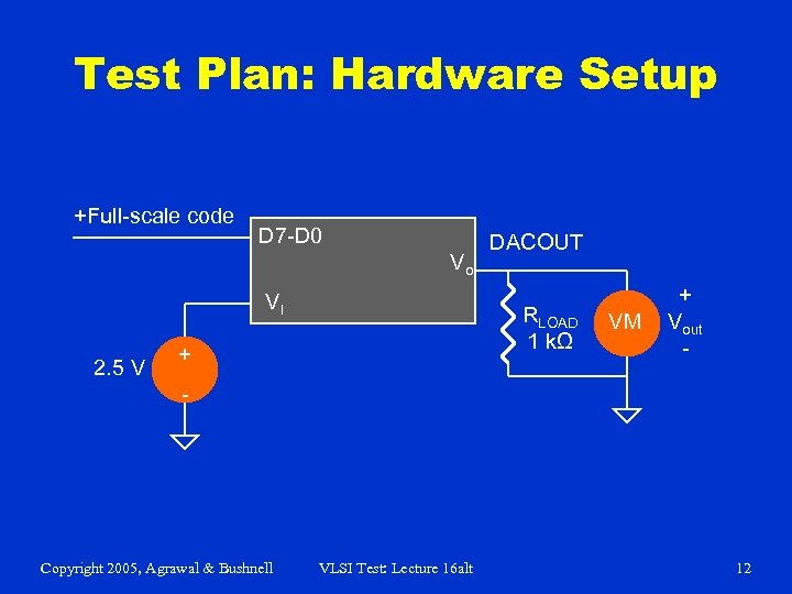 Test Plan: Hardware Setup +Full-scale code D 7 -D 0 Vo VI 2. 5 V DACOUT RLOAD 1 kΩ + VM + Vout - - Copyright 2005, Agrawal & Bushnell VLSI Test: Lecture 16 alt 12
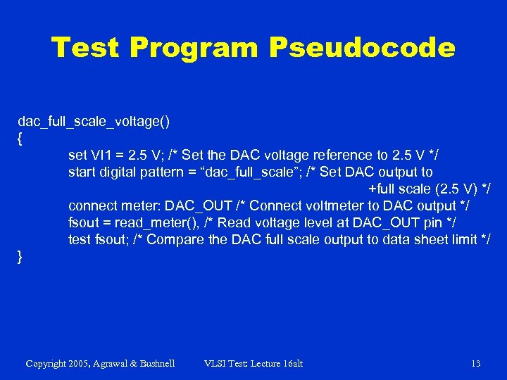 Test Program Pseudocode dac_full_scale_voltage() { set VI 1 = 2. 5 V; /* Set the DAC voltage reference to 2. 5 V */ start digital pattern = “dac_full_scale”; /* Set DAC output to +full scale (2. 5 V) */ connect meter: DAC_OUT /* Connect voltmeter to DAC output */ fsout = read_meter(), /* Read voltage level at DAC_OUT pin */ test fsout; /* Compare the DAC full scale output to data sheet limit */ } Copyright 2005, Agrawal & Bushnell VLSI Test: Lecture 16 alt 13
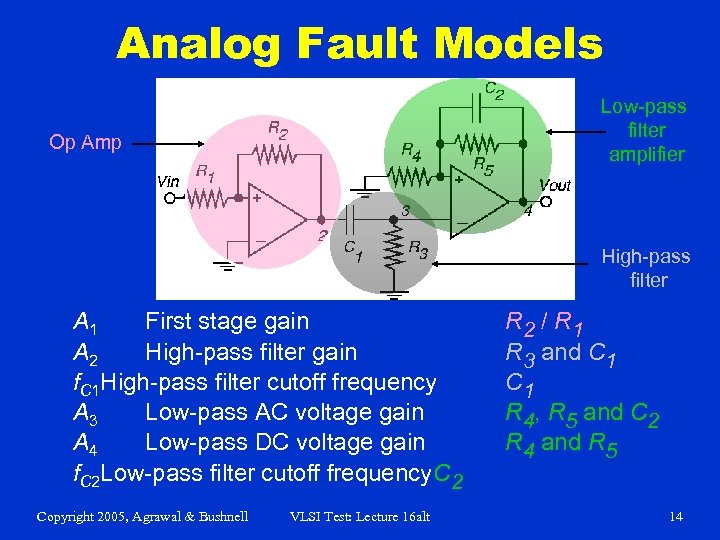 Analog Fault Models Low-pass filter amplifier Op Amp High-pass filter A 1 First stage gain A 2 High-pass filter gain f. C 1 High-pass filter cutoff frequency A 3 Low-pass AC voltage gain A 4 Low-pass DC voltage gain f. C 2 Low-pass filter cutoff frequency. C 2 Copyright 2005, Agrawal & Bushnell VLSI Test: Lecture 16 alt R 2 / R 1 R 3 and C 1 R 4, R 5 and C 2 R 4 and R 5 14
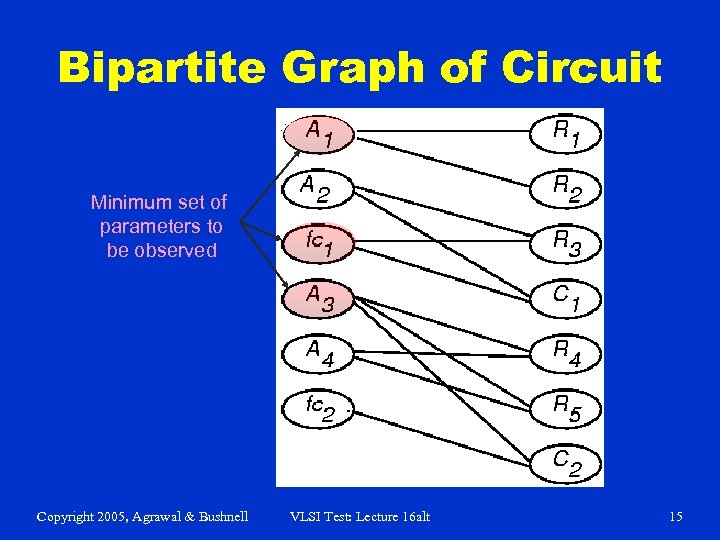 Bipartite Graph of Circuit Minimum set of parameters to be observed Copyright 2005, Agrawal & Bushnell VLSI Test: Lecture 16 alt 15
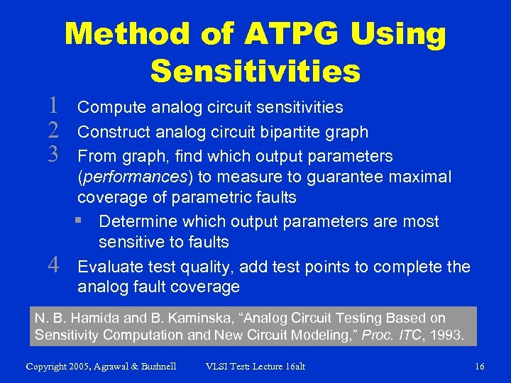 1 2 3 4 Method of ATPG Using Sensitivities Compute analog circuit sensitivities Construct analog circuit bipartite graph From graph, find which output parameters (performances) to measure to guarantee maximal coverage of parametric faults § Determine which output parameters are most sensitive to faults Evaluate test quality, add test points to complete the analog fault coverage N. B. Hamida and B. Kaminska, “Analog Circuit Testing Based on Sensitivity Computation and New Circuit Modeling, ” Proc. ITC, 1993. Copyright 2005, Agrawal & Bushnell VLSI Test: Lecture 16 alt 16
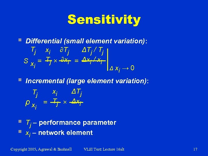 Sensitivity § Differential (small element variation): Tj xi ∂Tj ΔTj / Tj S x = Tj × ∂xi = Δxi / xi i Δ xi → 0 § Incremental (large element variation): Tj ρx i § § xi ΔTj = Tj × Δxi Tj – performance parameter xi – network element Copyright 2005, Agrawal & Bushnell VLSI Test: Lecture 16 alt 17
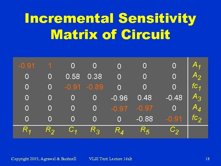 Incremental Sensitivity Matrix of Circuit -0. 91 0 0 0 R 1 1 0 0 0 R 2 0 0 0. 58 0. 38 -0. 91 -0. 89 0 0 0 C 1 R 3 Copyright 2005, Agrawal & Bushnell 0 0 0 -0. 96 -0. 97 0 R 4 VLSI Test: Lecture 16 alt 0 0. 48 -0. 97 -0. 88 R 5 0 0 0 -0. 48 0 -0. 91 C 2 A 1 A 2 fc 1 A 3 A 4 fc 2 18
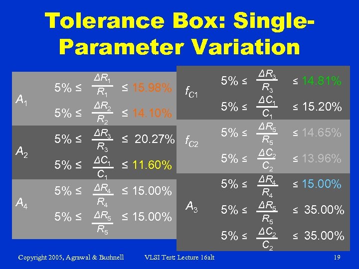 Tolerance Box: Single. Parameter Variation A 1 A 2 A 4 5% ≤ 5% ≤ ΔR 1 ΔR 2 ΔR 3 ΔC 1 ΔR 4 ΔR 5 ≤ 15. 98% f. C 1 5% ≤ ≤ 14. 10% ≤ 20. 27% f. C 2 5% ≤ ≤ 15. 00% Copyright 2005, Agrawal & Bushnell 5% ≤ ≤ 11. 60% ≤ 15. 00% 5% ≤ A 3 5% ≤ VLSI Test: Lecture 16 alt ΔR 3 ΔC 1 ΔR 5 ΔC 2 ΔR 4 ΔR 5 ΔC 2 ≤ 14. 81% ≤ 15. 20% ≤ 14. 65% ≤ 13. 96% ≤ 15. 00% ≤ 35. 00% 19
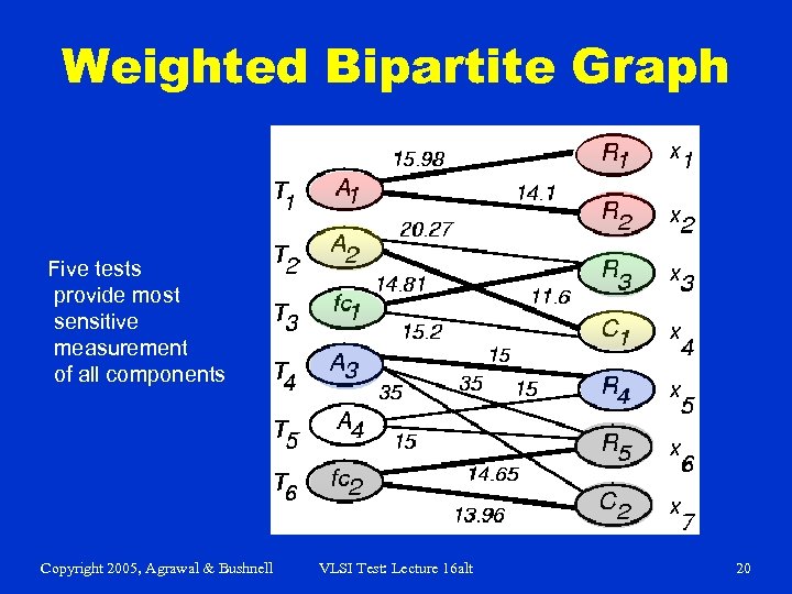 Weighted Bipartite Graph Five tests provide most sensitive measurement of all components Copyright 2005, Agrawal & Bushnell VLSI Test: Lecture 16 alt 20
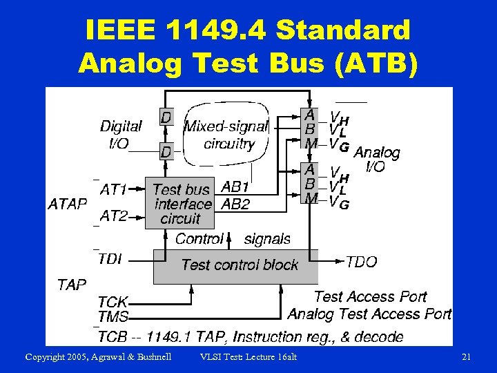 IEEE 1149. 4 Standard Analog Test Bus (ATB) Copyright 2005, Agrawal & Bushnell VLSI Test: Lecture 16 alt 21
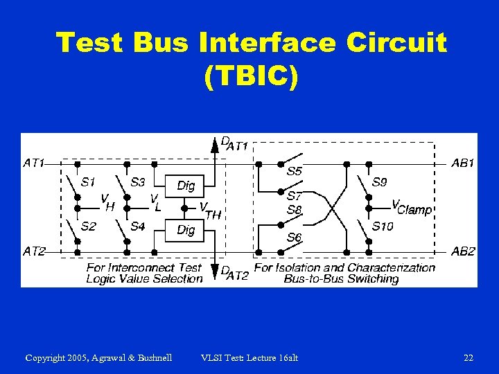 Test Bus Interface Circuit (TBIC) Copyright 2005, Agrawal & Bushnell VLSI Test: Lecture 16 alt 22
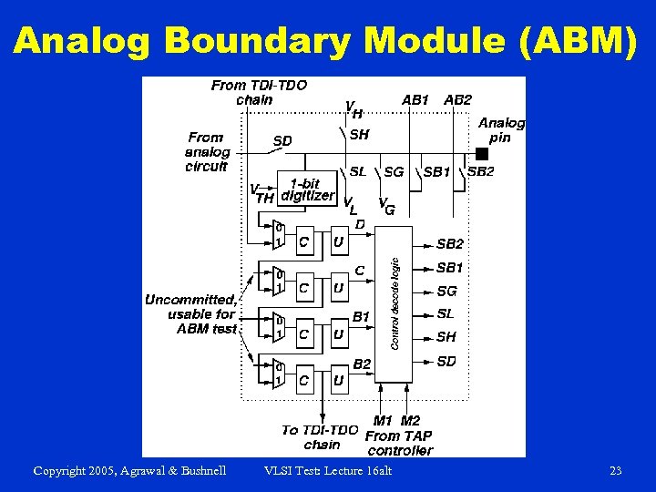 Analog Boundary Module (ABM) Copyright 2005, Agrawal & Bushnell VLSI Test: Lecture 16 alt 23
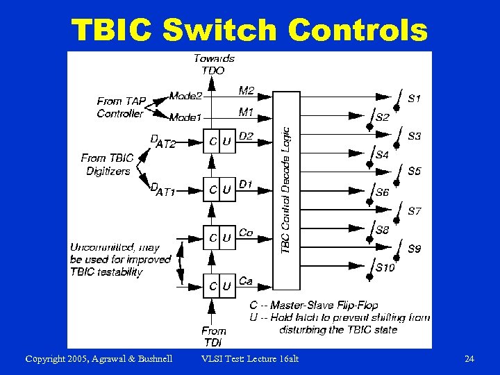 TBIC Switch Controls Copyright 2005, Agrawal & Bushnell VLSI Test: Lecture 16 alt 24
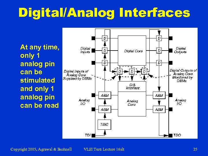 Digital/Analog Interfaces At any time, only 1 analog pin can be stimulated and only 1 analog pin can be read Copyright 2005, Agrawal & Bushnell VLSI Test: Lecture 16 alt 25
 Summary § § § DSP-based tester has: § Waveform synthesizer § Waveform digitizer § High frequency clock with dividers for synchronization Analog test methods § Specification-based functional testing § Model-based analog testing Analog test bus allows static analog tests of mixedsignal devices § Boundary scan is a prerequisite Copyright 2005, Agrawal & Bushnell VLSI Test: Lecture 16 alt 26
 References: Analog & RF Test § § § A. Afshar, Principles of Semiconductor Network Testing, Boston: Butterworth. Heinemann, 1995. M. Burns and G. Roberts, Introduction to Mixed-Signal IC Test and Measurement, New York: Oxford University Press, 2000. M. L. Bushnell and V. D. Agrawal, Essentials of Electronic Testing for Digital, Memory and Mixed-Signal VLSI Circuits, Boston: Springer, 2000. Chapters 10, 11 and 17. D. Gizopoulos, editor, Advances in Electronic Testing Challenges and Methodologies, Springer, 2006. Chapters 9 and 10. J. L. Huertas, editor, Test and Design-for-Testability in Mixed-Signal Integrated Circuits, Boston: Springer, 2004. P. Kabisatpathy, A Barua, and S. Sinha, Fault Diagnosis of Analog Integrated Circuits, Springer, 2005. R. W. Liu, editor, Testing and Diagnosis of Analog Circuits and Systems, New York: Van Nostrand Reinhold, 1991. M. Mahoney, DSP-Based Testing of Analog and Mixed-Signal Circuits, Los Alamitos, California: IEEE Computer Society Press, 1987. A. Osseiran, Analog and Mixed-Signal Boundary Scan, Boston: Springer, 1999. T. Ozawa, editor, Analog Methods for Computer-Aided Circuit Analysis and Diagnosis, New York: Marcel Dekker, 1988. K. B. Schaub and J. Kelly, Production Testing of RF and System-on-a-Chip Devices for Wireless Communications, Boston: Artech House, 2004. B. Vinnakota, editor, Analog and Mixed-Signal Test, Upper Saddle River, New Jersey: Prentice-Hall PTR, 1998. Copyright 2005, Agrawal & Bushnell VLSI Test: Lecture 16 alt 27


