753e4bd95151d2b249e2e41be8d0a47c.ppt
- Количество слайдов: 33

(Layer 0) Mechanical Issues + Test-Beams S. Bettarini On behalf of the Pisa Group V Super-B workshop – Paris 9 th May 2007
Outline • Support structure for a baseline striplet L 0 • For the APSEL MAPS candidate pixel sensor: – Mechanical/Thermal issues – Prototypes: micro-channel on Al. N substrate • “Looking for” a test-beam facility – The “demonstrator” • Conclusions
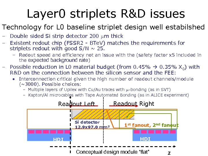
Layer 0 striplets R&D issues Technology for L 0 baseline striplet design well estabilshed – Double sided Si strip detector 200 mm thick – Existent redout chip (FSSR 2 - BTe. V) matches the requirements for striplets redout with good S/N ~ 25. – Redout speed and efficiency not an issue with the (safety factor x 5 included in the expected background rate) – Possible reduction in L 0 material budget (from 0. 45% 0. 35% X 0) with R&D on the connection between the silicon sensor and the FEE: • Interconnection critical given the high number of readout channels/module (~3000). Possible choices: – Multiple layers of Upilex with Cu/Au traces with m-bonding (as in SVT) – Kapton/Al microcables with Tape Automated Bonding (as in ALICE experiment) Readout Left Si detector 12. 9 x 97. 0 mm 2 HDI Readout Right 1 st fanout, 2 nd fanout HDI Conceptual design module “flat” z
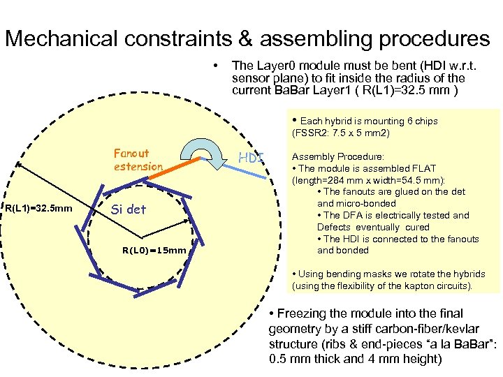
Mechanical constraints & assembling procedures • The Layer 0 module must be bent (HDI w. r. t. sensor plane) to fit inside the radius of the current Ba. Bar Layer 1 ( R(L 1)=32. 5 mm ) • Each hybrid is mounting 6 chips (FSSR 2: 7. 5 x 5 mm 2) Fanout estension R(L 1)=32. 5 mm Si det R(L 0)=15 mm HDI Assembly Procedure: • The module is assembled FLAT (length=284 mm x width=54. 5 mm): • The fanouts are glued on the det and micro-bonded • The DFA is electrically tested and Defects eventually cured • The HDI is connected to the fanouts and bonded • Using bending masks we rotate the hybrids (using the flexibility of the kapton circuits). • Freezing the module into the final geometry by a stiff carbon-fiber/kevlar structure (ribs & end-pieces “a la Ba. Bar”: 0. 5 mm thick and 4 mm height)
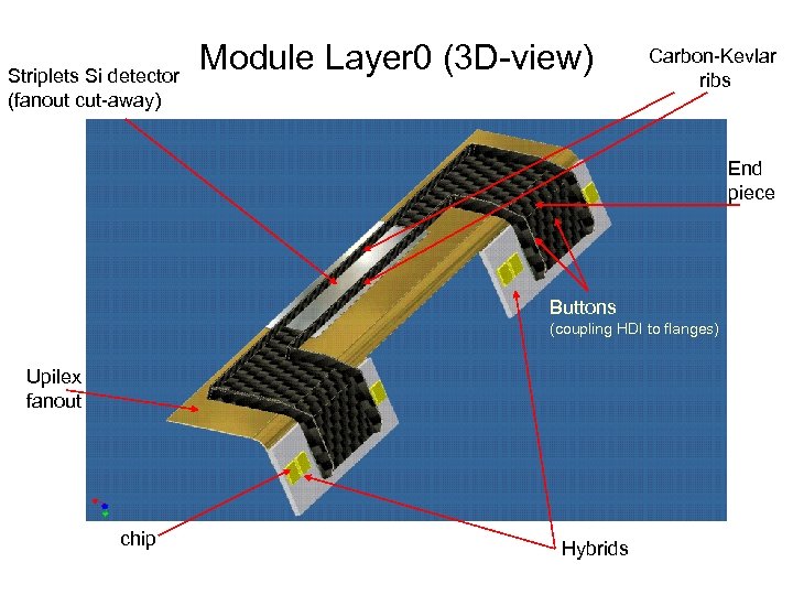
Striplets Si detector (fanout cut-away) Module Layer 0 (3 D-view) Carbon-Kevlar ribs End piece Buttons (coupling HDI to flanges) Upilex fanout chip Hybrids
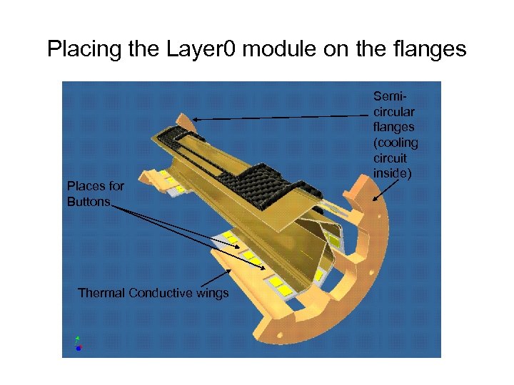
Placing the Layer 0 module on the flanges Places for Buttons Thermal Conductive wings Semicircular flanges (cooling circuit inside)
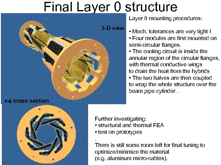
Final Layer 0 structure Layer 0 mounting procedures: 3 -D view • Mech. tolerances are very tight ! • Four modules are first mounted on semi-circular flanges. • The cooling circuit is inside the annular region of the circular flanges, with thermal conductive wings to drain the heat from the hybrids • The two halves are then coupled to wrap the whole structure over the beam pipe cylinder. r-f cross section Further investigating: • structural and thermal FEA • test on prototypes. There is still some room left for final tuning to optimize/minimize the material (e. g. aluminum micro-cables).
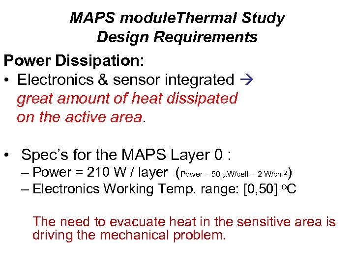
MAPS module. Thermal Study Design Requirements Power Dissipation: • Electronics & sensor integrated great amount of heat dissipated on the active area. • Spec’s for the MAPS Layer 0 : – Power = 210 W / layer (Power = 50 m. W/cell = 2 W/cm ) – Electronics Working Temp. range: [0, 50] o. C 2 The need to evacuate heat in the sensitive area is driving the mechanical problem.
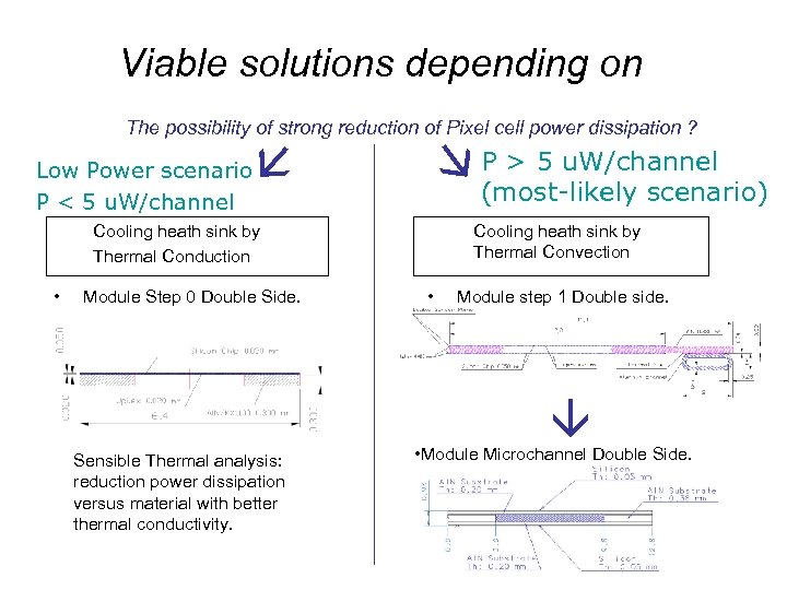
Viable solutions depending on Low Power scenario P < 5 u. W/channel The possibility of strong reduction of Pixel cell power dissipation ? Cooling heath sink by Thermal Conduction • Module Step 0 Double Side. P > 5 u. W/channel (most-likely scenario) Cooling heath sink by Thermal Convection • Module step 1 Double side. Sensible Thermal analysis: reduction power dissipation versus material with better thermal conductivity. • Module Microchannel Double Side.
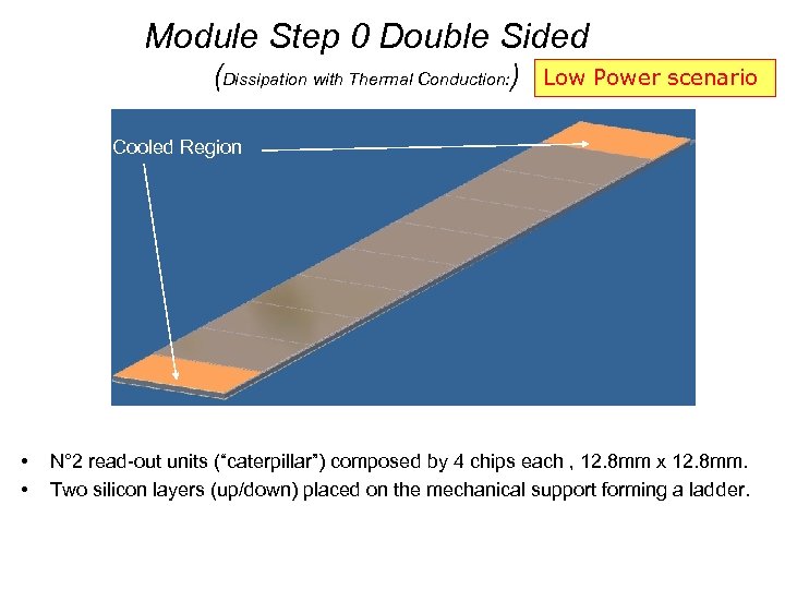
Module Step 0 Double Sided (Dissipation with Thermal Conduction: ) Low Power scenario Cooled Region • • N° 2 read-out units (“caterpillar”) composed by 4 chips each , 12. 8 mm x 12. 8 mm. Two silicon layers (up/down) placed on the mechanical support forming a ladder.
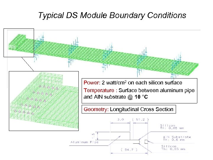
Typical DS Module Boundary Conditions Power: 2 watt/cm 2 on each silicon surface Temperature : Surface between aluminum pipe and Al. N substrate @ 10 °C Geometry: Longitudinal Cross Section
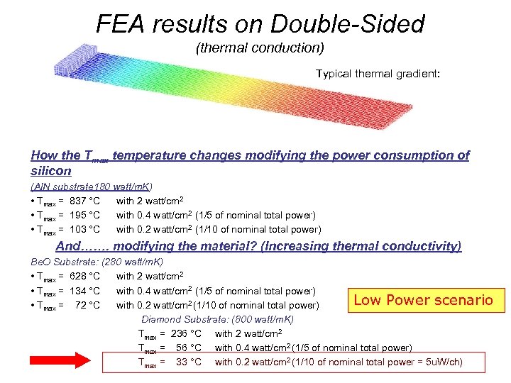
FEA results on Double-Sided (thermal conduction) Typical thermal gradient: How the Tmax temperature changes modifying the power consumption of silicon (Al. N substrate 180 watt/m. K) • Tmax = 837 °C with 2 watt/cm 2 • Tmax = 195 °C with 0. 4 watt/cm 2 (1/5 of nominal total power) • Tmax = 103 °C with 0. 2 watt/cm 2 (1/10 of nominal total power) And……. modifying the material? (Increasing thermal conductivity) Be. O Substrate: (280 watt/m. K) • Tmax = 628 °C with 2 watt/cm 2 • Tmax = 134 °C with 0. 4 watt/cm 2 (1/5 of nominal total power) Low Power scenario • Tmax = 72 °C with 0. 2 watt/cm 2 (1/10 of nominal total power) Diamond Substrate: (800 watt/m. K) Tmax = 236 °C with 2 watt/cm 2 Tmax = 56 °C with 0. 4 watt/cm 2 (1/5 of nominal total power) Tmax = 33 °C with 0. 2 watt/cm 2 (1/10 of nominal total power = 5 u. W/ch)
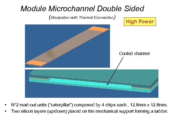
Module Microchannel Double Sided (Dissipation with Thermal Convection) High Power Cooled channel • • N° 2 read-out units (“caterpillar”) composed by 4 chips each , 12. 8 mm x 12. 8 mm. Two silicon layers (up/down) placed on the mechanical support forming a ladder.
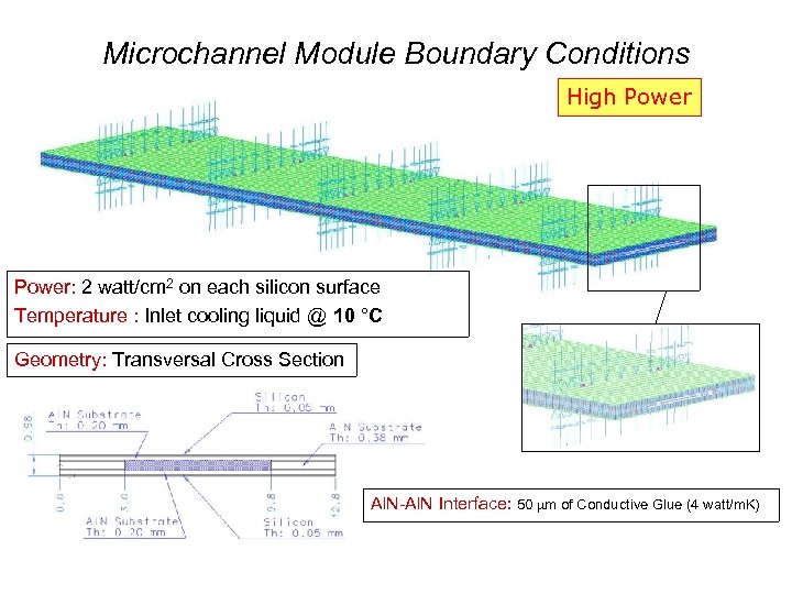
Microchannel Module Boundary Conditions High Power: 2 watt/cm 2 on each silicon surface Temperature : Inlet cooling liquid @ 10 °C Geometry: Transversal Cross Section Al. N-Al. N Interface: 50 mm of Conductive Glue (4 watt/m. K)
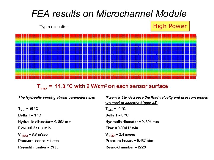
FEA results on Microchannel Module High Power Typical results: Tmax = 11. 3 °C with 2 W/cm 2 on each sensor surface The Hydraulic cooling circuit parameters are: If we want to decrease the fluid velocity and pressure losses we need to accept a bigger DT. Tinlet = 10 °C Delta T = 3 °C Delta T = 8 °C Hydraulic diameter = 0. 897 mm Flow = 0. 251 l / min Flow = 0. 094 l / min V (H 2 O) = 6. 6 m/sec V (H 2 O) = 2. 5 m/sec Pressure losses = 1 atm Pressure losses = 0. 187 atm Reynold number = 5933 Reynold number = 2225
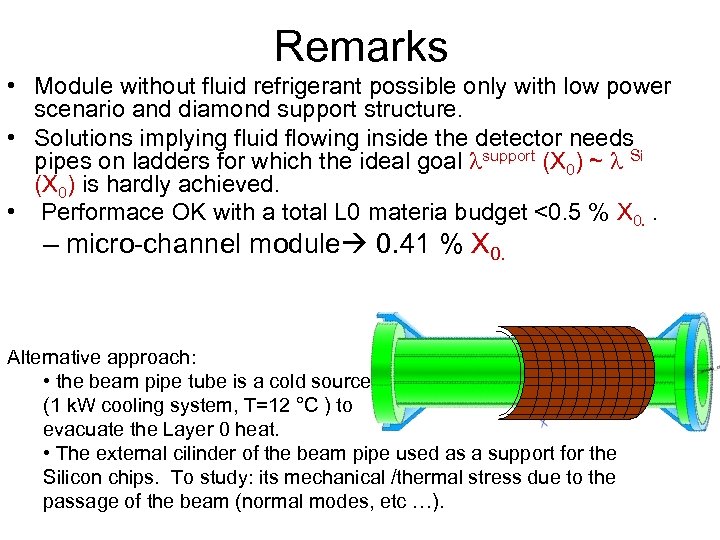
Remarks • Module without fluid refrigerant possible only with low power scenario and diamond support structure. • Solutions implying fluid flowing inside the detector needs pipes on ladders for which the ideal goal lsupport (X 0) ~ l Si (X 0) is hardly achieved. • Performace OK with a total L 0 materia budget <0. 5 % X 0. . – micro-channel module 0. 41 % X 0. Alternative approach: • the beam pipe tube is a cold source (1 k. W cooling system, T=12 °C ) to evacuate the Layer 0 heat. • The external cilinder of the beam pipe used as a support for the Silicon chips. To study: its mechanical /thermal stress due to the passage of the beam (normal modes, etc …).
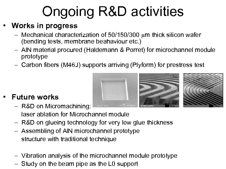
Ongoing R&D activities • Works in progress – Mechanical characterization of 50/150/300 mm thick silicon wafer (bending tests, membrane beahaviour etc. ) – Al. N material procured (Haldemann & Porret) for microchannel module prototype – Carbon fibers (M 46 J) supports arriving (Plyform) for prestress test • Future works – R&D on Micromachining: laser ablation for Microchannel module – R&D on glueing technology for very low glue thickness – Assembling of Al. N microchannel prototype structure with traditional technique – Vibration analysis of the microchannel module prototype – Study on the beam pipe as the L 0 support
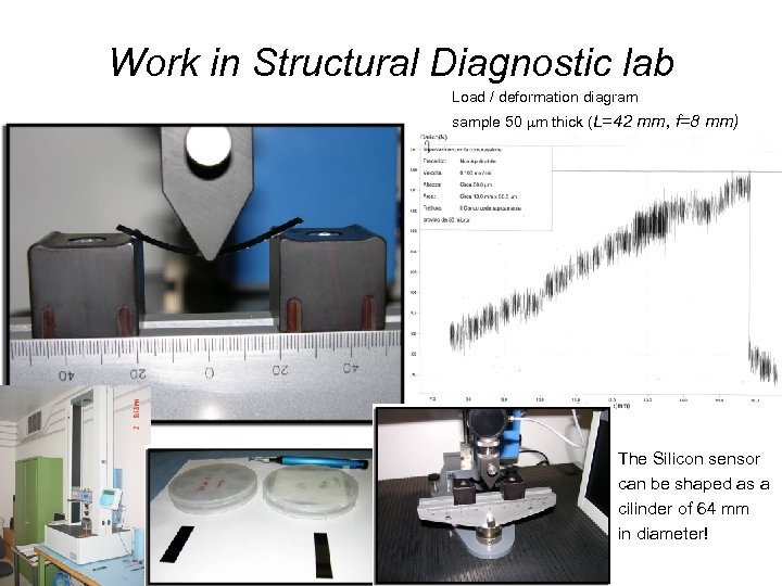
Work in Structural Diagnostic lab Load / deformation diagram sample 50 mm thick (L=42 mm, f=8 mm) The Silicon sensor can be shaped as a cilinder of 64 mm in diameter!
Test-beam in 2008 • In the 2 nd half of 2008 MAPS and striplet detectors ready to be tested on the beam • Still looking for the best site. • Test of the whole system, consisting of: – Sensor MAPS – DSSD striplets – Read-out (FSSR 2) – DAQ/AM
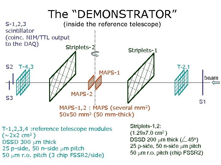
The “DEMONSTRATOR” S-1, 2, 3 (inside the reference telescope) scintillator (coinc. NIM/TTL output to the DAQ) Striplets-2 Striplets-1 S 2 S 3 T-4, 3 T-2, 1 MAPS-1 beam MAPS-2 MAPS-1, 2 : MAPS (several mm 2) 50 x 50 mm 2 (50 mm-thick) T-1, 2, 3, 4 : reference telescope modules (~2 x 2 cm 2 ) DSSD 300 mm thick 25 p-side, 50 n-side mm pitch 50 mm r. o. pitch (3 chip FSSR 2/side) S 1 Striplets-1, 2: (1. 29 x 7. 0 cm 2 ) DSSD 200 mm thick ( 45 o) 25 p-side, 50 n-side mm pitch 50 mm r. o. pitch (chip FSSR 2)
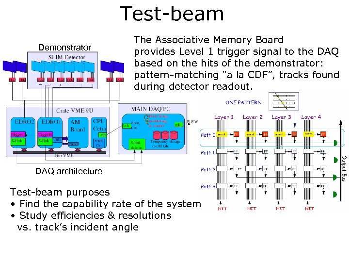
Test-beam Demonstrator The Associative Memory Board provides Level 1 trigger signal to the DAQ based on the hits of the demonstrator: pattern-matching “a la CDF”, tracks found during detector readout. DAQ architecture Test-beam purposes • Find the capability rate of the system • Study efficiencies & resolutions vs. track’s incident angle
Conclusions • Provided a working design for the striplet L 0 • R&D ongoing for the mechanical/thermal issues of the pixel L 0 with the CMOS MAPS sensor. Focus on: – power dissipation – minimize the material The spec’s of the problem are defined: room for new ideas and mechanical solutions! • Series of test-beams for the demonstrator (1 st starting in summer 2008 and then in 2009) Looking for the best test-beam facility.

Back-up SLIDES
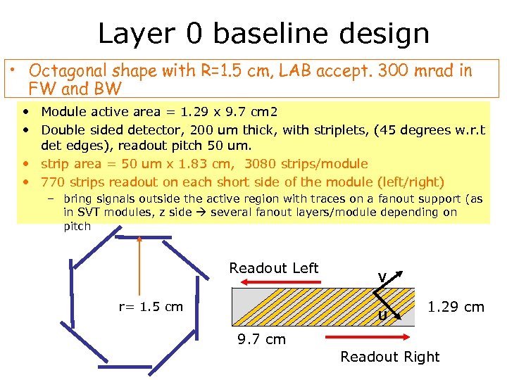
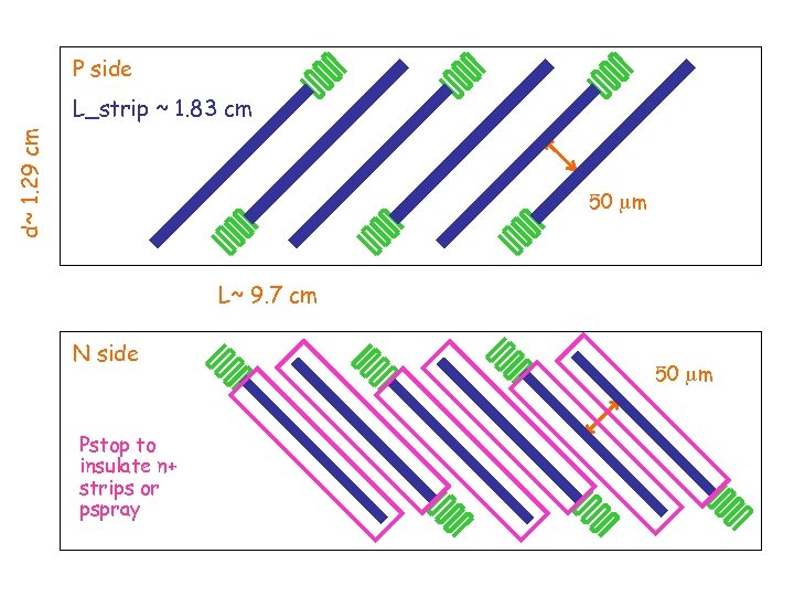
Layer 0 baseline design • Octagonal shape with R=1. 5 cm, LAB accept. 300 mrad in FW and BW • Module active area = 1. 29 x 9. 7 cm 2 • Double sided detector, 200 um thick, with striplets, (45 degrees w. r. t det edges), readout pitch 50 um. • strip area = 50 um x 1. 83 cm, 3080 strips/module • 770 strips readout on each short side of the module (left/right) – bring signals outside the active region with traces on a fanout support (as in SVT modules, z side several fanout layers/module depending on pitch Readout Left r= 1. 5 cm V U 1. 29 cm 9. 7 cm Readout Right
P side d~ 1. 29 cm L_strip ~ 1. 83 cm 50 mm L~ 9. 7 cm N side Pstop to insulate n+ strips or pspray 50 mm
Front end chip I • Expected background hit rate = 5 MHz/cm 2 @ r=1. 5 cm – Including x 10 safety factor 50 MHz/cm 2 used in the following • L 0 strip rates (> 450 k. Hz) are not acceptable with present SVT front end (ATOM chip) : – With 1 ms readout window L 0 strip occupancy > 45% – Inefficiency due to shadowing: a single hit (the first in the readout window) is retrieved from the pipeline when LV 1 trigger is received background hits can shadow hits from physics – Such a high occupancy affects pattern recognition
Front end chip II • Try a different approach for readout: fast, data driven readout architecture, with no analog storage, with enough output bandwidth to ensure that no data is lost due to readout deadtime. • FSSR 2, designed for the BTe. V Forward Silicon Tracker (Pavia/Bergamo-Fermilab), has the right features: – Mixed-signal integrated circuit for the readout of silicon strip detectors (selectable shaper peaking time: 65 -85 -125 ns) – TSMC 0. 25 µm CMOS tech. with enclosed NMOS Rad. Hard – 128 analog channels, sparsified digital output with address, timestamp, and pulse height information for all hits Architecture designed to run with 132 ns bunch crossing (timestamp granularity = BCO clock = 7. 6 MHz), readout clock @ 70 MHz 840 Mb/s output data rate. For more details on FSSR 2 see for example: – – • V. Re et al. , “FSSR 2, a Self-Triggered Low Noise Readout Chip for Silicon Strip Detectors”, 2005 IEEE Nuclear Science Symposium Conference Record • V. Re: “First prototype of a silicon microstrip detector with the data-driven readout chip FSSR 2 for a tracking-based trigger system” , presented @ 10 th Pisa Meeting on Advanced Detectors, La Biodola (Isola d’Elba), May 21 – 27, 2006
FSSR 2 for L 0 striplets • In Super. B L 0 expected FSSR 2 chip occupancy (132 ns) = 6% – Should be OK for pattern recognition – Is FSSR 2 fast enough for Super. B? – YES, if you believe to simulation performed for BTe. V • FSSR 2 chip optimized for BTe. V operation: – With 2 interactions/bunch crossing (132 ns), expected BTe. V FSSR 2 occupancy 2% – With standard operation (132 ns BCO clock) FSSR 2 can handle 2% occupancy with efficiency > 99%. • FSSR 2 Simulation performed for BTe. V with 6% occupancy (6 interactions/bunch crossing) indicates: – Efficiency ~ 96. 5%, with standard BCO clock frequency – Can improve efficiency (~ 98. 5%) with x 4 BCO clock frequency. • FSSR 2 chip can read L 0 striplets (6% occupancy) with 98. 5% efficiency
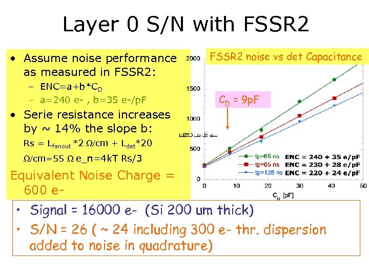
Layer 0 S/N with FSSR 2 • Assume noise performance as measured in FSSR 2: – ENC=a+b*CD – a=240 e- , b=35 e-/p. F • Serie resistance increases by ~ 14% the slope b: FSSR 2 noise vs det Capacitance CD = 9 p. F Rs = Lfanout *2 /cm + Ldet*20 /cm=55 e_n=4 k. T Rs/3 Equivalent Noise Charge = 600 e- • Signal = 16000 e- (Si 200 um thick) • S/N = 26 ( ~ 24 including 300 e- thr. dispersion added to noise in quadrature)
Radiation Hardness • Si detector dose ~ 6. 6 Mrad/yr (safety included). Should be ok (rough estimate of noise contribution due to leakage current ~ 670 e- after 5 years of operation, to be added in quadrature to previous noise figure). • Chip dose depends on their radial location. – Assuming chip located at radius of ~ 2. 4 cm expected chip dose ~ 200 krad/yr OK ! FSSR 2 < Irradiation with 60 Co g-rays to a total ionizing dose of 20 Mrad (no bias applied during irradiation) < Chip fully functional after irradiation; noise and charge sensitivity are not affected < Threshold dispersion with BLR selected increases by about 15 % (remains below the spec value of 500 e rms)
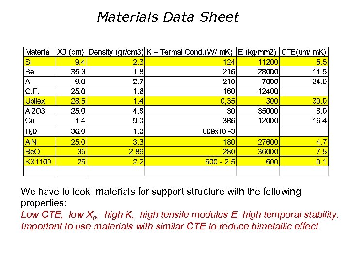
Materials Data Sheet We have to look materials for support structure with the following properties: Low CTE, low X 0, high K, high tensile modulus E, high temporal stability. Important to use materials with similar CTE to reduce bimetallic effect.
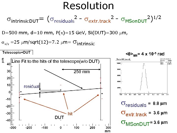
Resolution sintrinsic. DUT= (sresiduals 2 - sextr. track 2 - s. MSon. DUT 2)1/2 D=500 mm, d=10 mm, P(p)=15 Ge. V, Si(DUT)=300 mm, sx/y =25 mm/sqrt(12)=7. 2 mm= sintrinsic <q>MS= 4 x 10 -5 rad Line Fit to the hits of the telescope(w/o DUT) 250 mm residual DUT hit sresiduals = 8. 8 mm sextr. track = 3. 6 mm s. MSon. DUT= 3. 6 mm
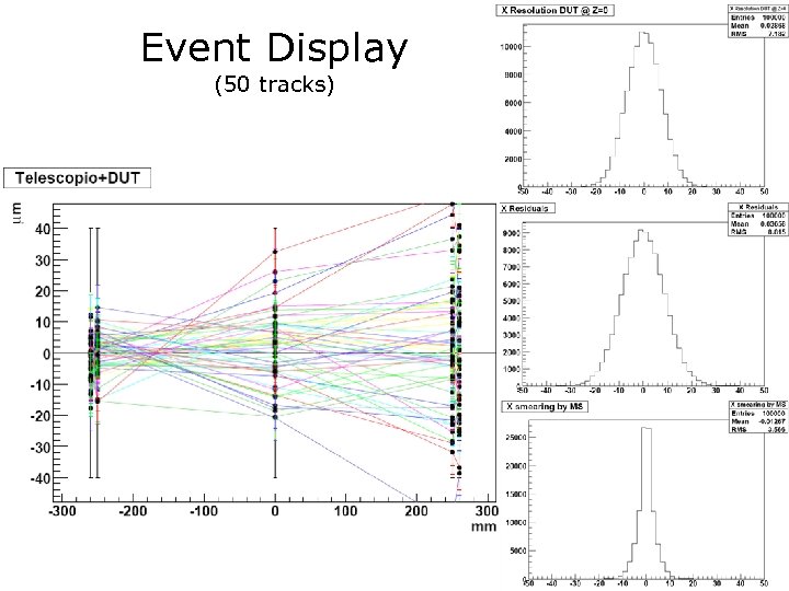
Event Display (50 tracks)
753e4bd95151d2b249e2e41be8d0a47c.ppt