570046583761c76b4f60b9efe93a6332.ppt
- Количество слайдов: 46
 LARGE AREA TRANSITION-EDGE SENSOR ARRAY FOR PARTICLE INDUCED X-RAY EMISSION SPECTROSCOPY M Palosaari 1, K Kinnunen 1, I Maasilta 1, C Reintsema 2, D Schmidt 2, J Fowler 2, R Doriese 2, J Ullom 2, M Käyhkö 1, J Julin 1, Mikko Laitinen 1, T Sajavaara 1 1 Department 2 National of Physics, University of Jyväskylä, P. O. Box 35, Jyväskylä 40014, Finland Institute of Standards and Technology, Boulder CO 80305, United States email: mikko. i. laitinen@jyu. fi
 INTRODUCTION TO TES SUPERCONDUCTING TRANSITION-EDGE SENSOR
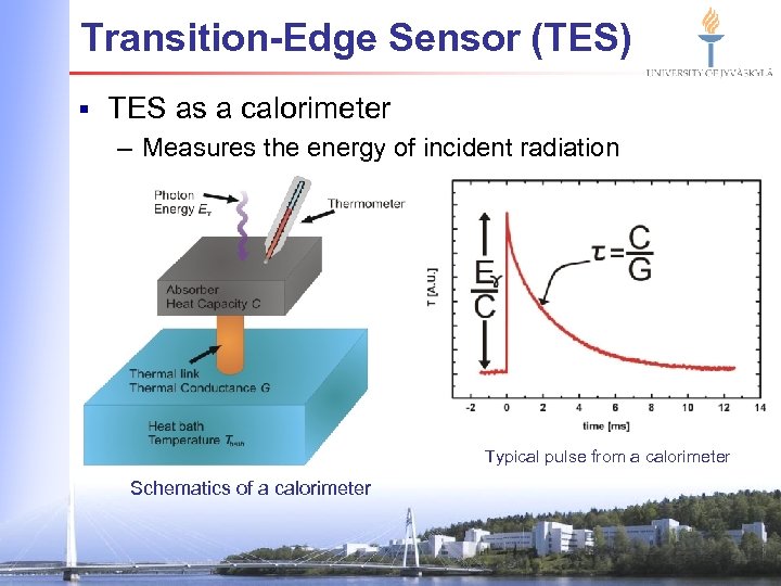 Transition-Edge Sensor (TES) § TES as a calorimeter – Measures the energy of incident radiation Typical pulse from a calorimeter Schematics of a calorimeter
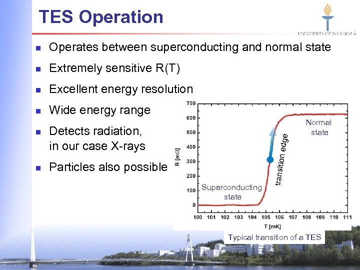 TES Operation n Operates between superconducting and normal state n Extremely sensitive R(T) n Excellent energy resolution n Wide energy range n edge Detects radiation, in our case X-rays Particles also possible Superconducting state transition n Normal state Typical transition of a TES
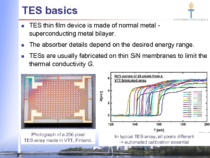 TES basics n n n TES thin film device is made of normal metal superconducting metal bilayer. The absorber details depend on the desired energy range. TESs are usually fabricated on thin Si. N membranes to limit thermal conductivity G. Photograph of a 256 pixel TES array made in VTT, Finland. In typical TES array, all pixels different -> automated calibration essential
 PIXE-TES SETUP IN JYVÄSKYLÄ
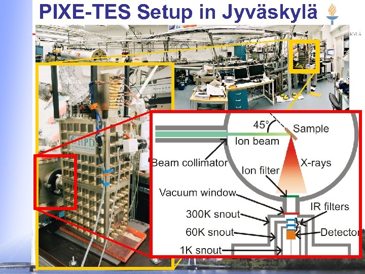 PIXE-TES Setup in Jyväskylä
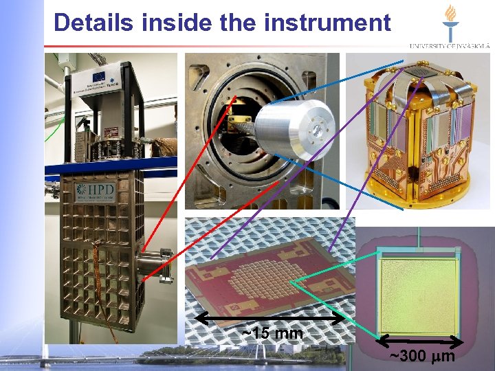 Details inside the instrument ~15 mm ~300 mm
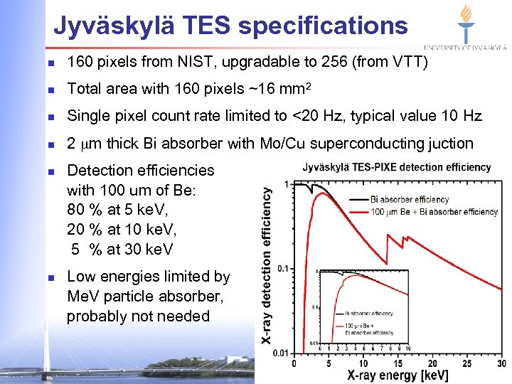 Jyväskylä TES specifications n 160 pixels from NIST, upgradable to 256 (from VTT) n Total area with 160 pixels ~16 mm 2 n Single pixel count rate limited to <20 Hz, typical value 10 Hz n 2 mm thick Bi absorber with Mo/Cu superconducting juction n n Detection efficiencies with 100 um of Be: 80 % at 5 ke. V, 20 % at 10 ke. V, 5 % at 30 ke. V Low energies limited by Me. V particle absorber, probably not needed
 PIXE-TES MEASUREMENTS FROM A SINGLE PIXEL TO MANY…
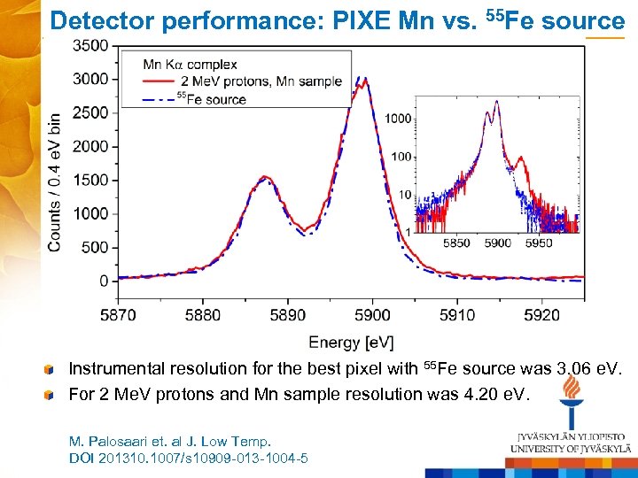
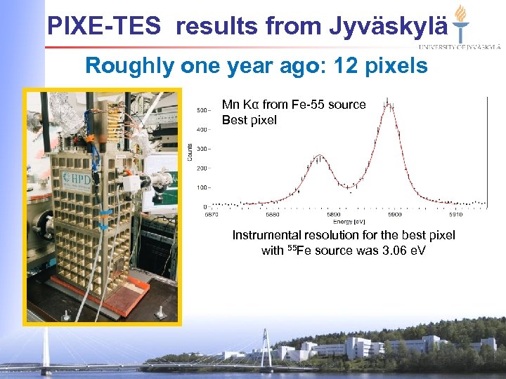 PIXE-TES results from Jyväskylä Roughly one year ago: 12 pixels Mn Kα from Fe-55 source Best pixel Instrumental resolution for the best pixel with 55 Fe source was 3. 06 e. V
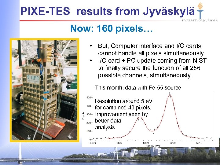 PIXE-TES results from Jyväskylä Now: 160 pixels… • But, Computer interface and I/O cards cannot handle all pixels simultaneously • I/O card + PC update coming from NIST to finally secure the function of all 256 possible channels, simultaneously. This month: data with Fe-55 source Resolution around 5 e. V for combined 40 pixels, Improvement seen by better data analysis
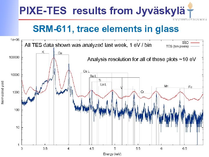 PIXE-TES results from Jyväskylä SRM-611, trace elements in glass All TES data shown was analyzed last week, 1 e. V / bin Analysis resolution for all of these plots ~10 e. V
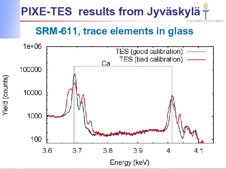 PIXE-TES results from Jyväskylä SRM-611, trace elements in glass
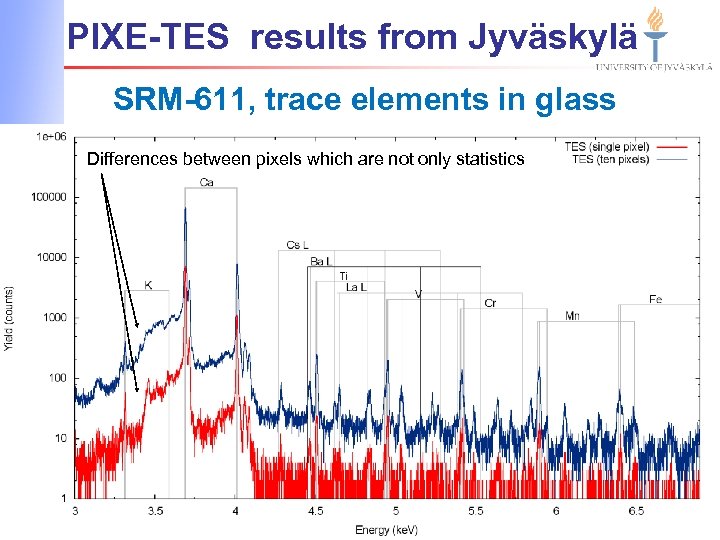 PIXE-TES results from Jyväskylä SRM-611, trace elements in glass Differences between pixels which are not only statistics
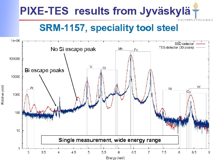 PIXE-TES results from Jyväskylä SRM-1157, speciality tool steel No Si escape peak Bi escape peaks Single measurement, wide energy range
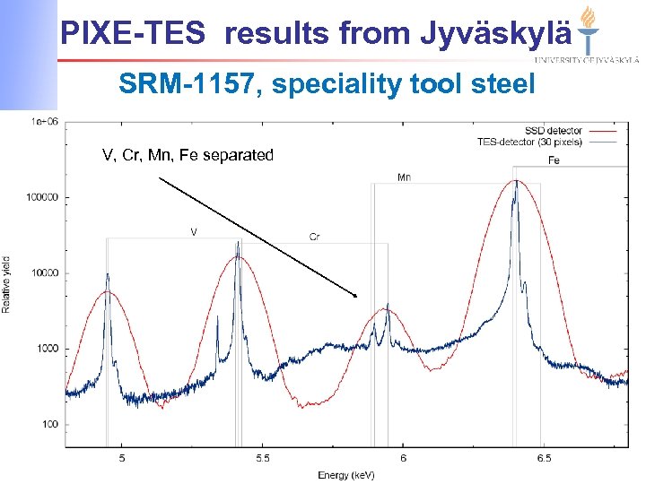 PIXE-TES results from Jyväskylä SRM-1157, speciality tool steel V, Cr, Mn, Fe separated
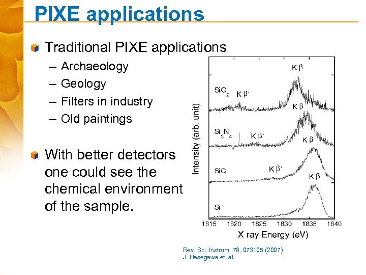
 In the Near Future n n Read-out upgraded to full scale. Modification of PIXE setup to be able to measure samples in atmosphere. n n n Study art samples in a project that just started X-ray measurements with our own detector array fabricated by VTT. Study the satellite peaks with different ions and energies. n ->> Chemical information from wide energy/elemental range ? ? ?
 Conclusions n Instrumental resolution of 3 e. V demonstrated n Combined pixel resolution of ~5 e. V looks realistic n Wide energy scale (“ 0” to tens of ke. V) n Reasonable count rates available (10 Hz/pixel, 256 pixels) n Active detector area about 16 mm 2 n No liquid He needed for ADR cryo cooler n Largish instrument: ~5 cm sample-to-detector n Data handling and analysis: automation necessary n Is the chemical information achievable, after all ?
 Acknowledgements
 t 3 -8. July, 2016, in Jyväskylä, Finland
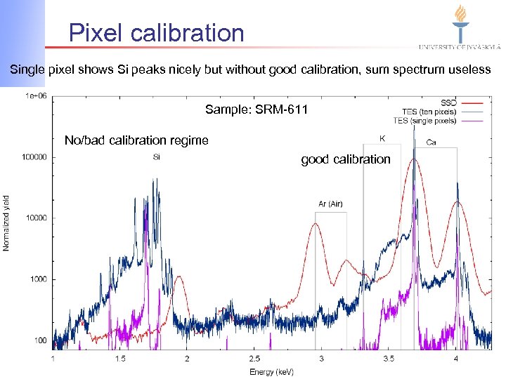 Pixel calibration Single pixel shows Si peaks nicely but without good calibration, sum spectrum useless Sample: SRM-611 No/bad calibration regime good calibration
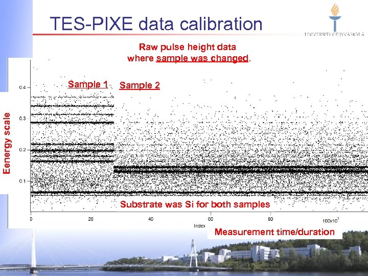 TES-PIXE data calibration Raw pulse height data where sample was changed. Sample 2 Eenergy scale Sample 1 Substrate was Si for both samples Measurement time/duration
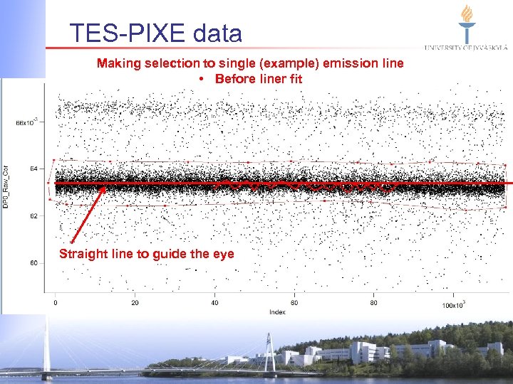 TES-PIXE data Making selection to single (example) emission line • Before liner fit Straight line to guide the eye
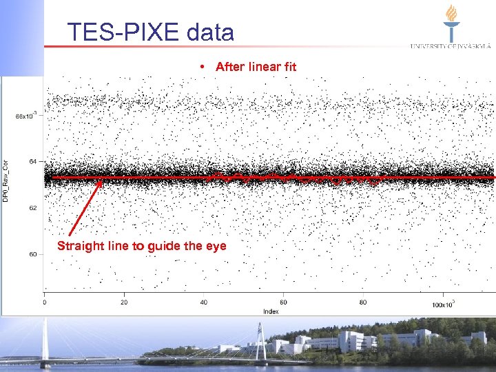 TES-PIXE data • After linear fit Si Straight line to guide the eye Si
 Nitride hits
 PIXE Mn vs. 55 Fe Mn Kα from Fe 55 source same pixel What is the origin of the hump?
 Detector performance: PIXE Mn vs. 55 Fe source Instrumental resolution for the best pixel with 55 Fe source was 3. 06 e. V. For 2 Me. V protons and Mn sample resolution was 4. 20 e. V. M. Palosaari et. al J. Low Temp. DOI 201310. 1007/s 10909 -013 -1004 -5
 PIXE applications Traditional PIXE applications – – Archaeology Geology Filters in industry Old paintings With better detectors one could see the chemical environment of the sample. Rev. Sci. Instrum. 78, 073105 (2007) J. Hasegawa et. al
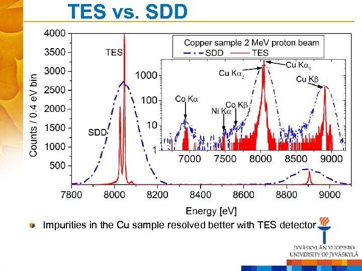 TES vs. SDD Impurities in the Cu sample resolved better with TES detector
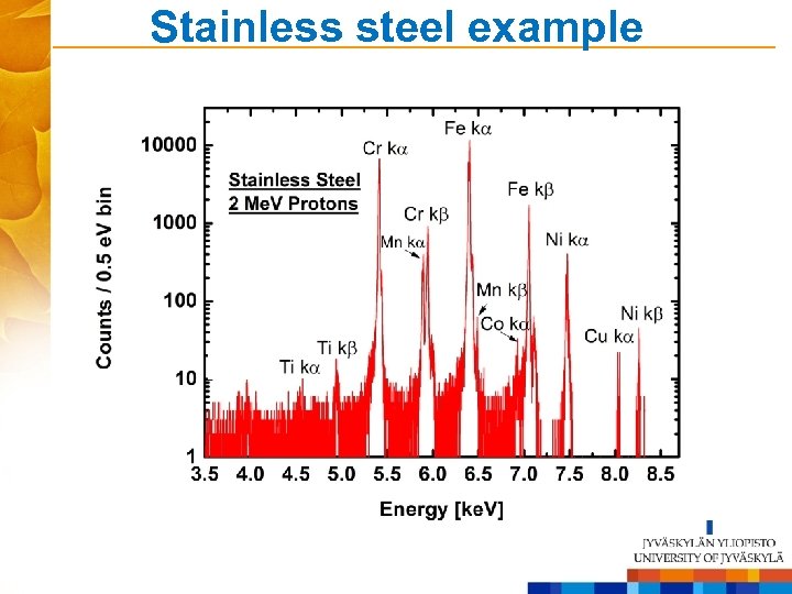 Stainless steel example
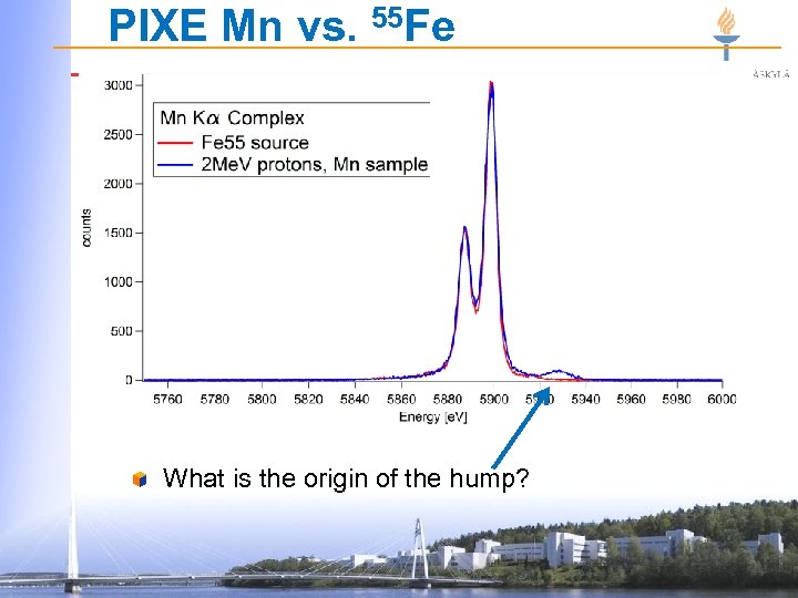
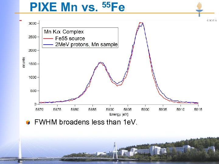 PIXE Mn vs. 55 Fe Mn Kα from Fe 55 source same pixel FWHM broadens less than 1 e. V.
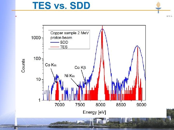 TES vs. SDD
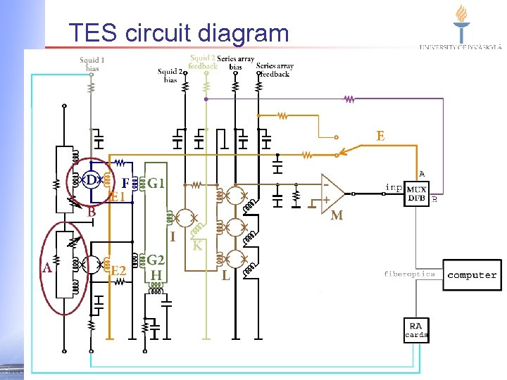 TES circuit diagram
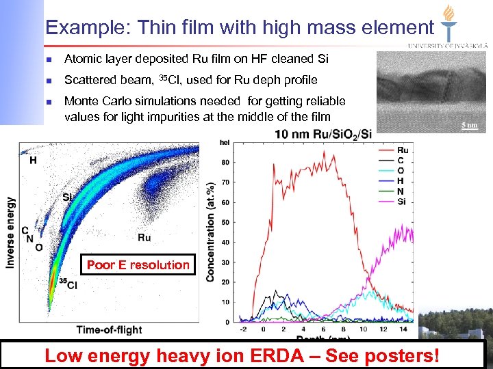 Example: Thin film with high mass element n Atomic layer deposited Ru film on HF cleaned Si n Scattered beam, 35 Cl, used for Ru deph profile n Ru Monte Carlo simulations needed for getting reliable values for light impurities at the middle of the film Si. O 2 Si Poor E resolution Low energy heavy ion ERDA – See posters!
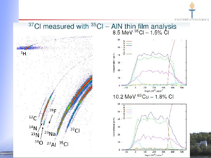
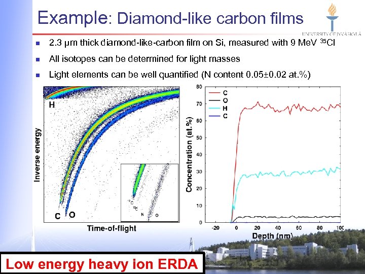 Example: Diamond-like carbon films n 2. 3 µm thick diamond-like-carbon film on Si, measured with 9 Me. V 35 Cl n All isotopes can be determined for light masses n Light elements can be well quantified (N content 0. 05± 0. 02 at. %) Low energy heavy ion ERDA
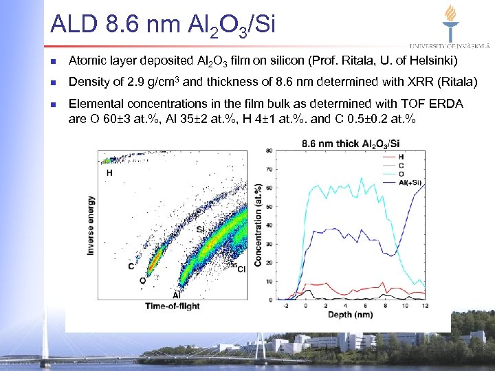 ALD 8. 6 nm Al 2 O 3/Si n Atomic layer deposited Al 2 O 3 film on silicon (Prof. Ritala, U. of Helsinki) n Density of 2. 9 g/cm 3 and thickness of 8. 6 nm determined with XRR (Ritala) n Elemental concentrations in the film bulk as determined with TOF ERDA are O 60± 3 at. %, Al 35± 2 at. %, H 4± 1 at. %. and C 0. 5± 0. 2 at. %
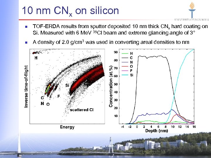 10 nm CNx on silicon n n TOF-ERDA results from sputter deposited 10 nm thick CNx hard coating on Si. Measured with 6 Me. V 35 Cl beam and extreme glancing angle of 3° A density of 2. 0 g/cm 3 was used in converting areal densities to nm
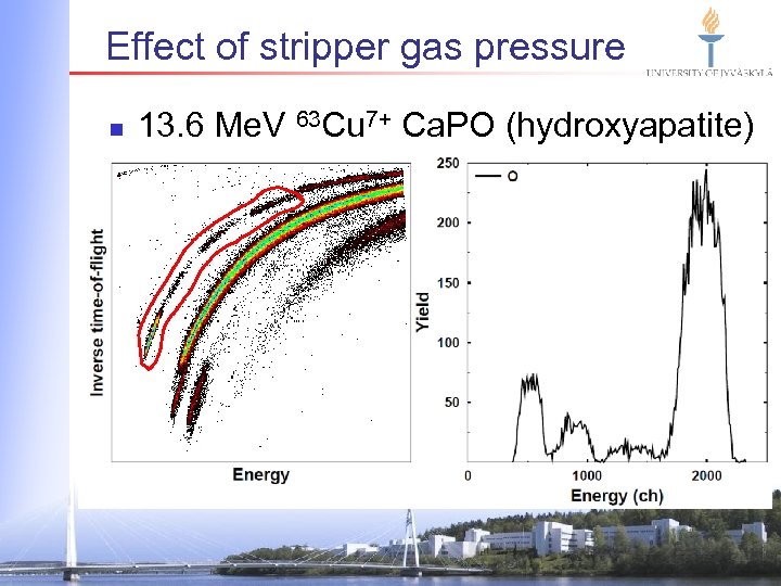 Effect of stripper gas pressure n 13. 6 Me. V 63 Cu 7+ Ca. PO (hydroxyapatite)
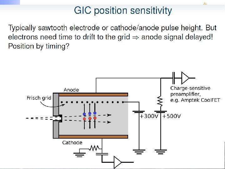
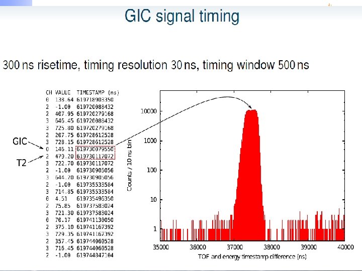
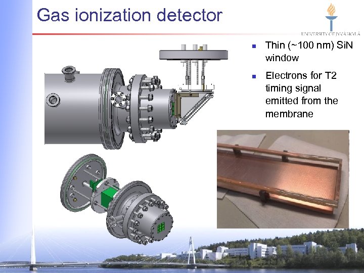 Gas ionization detector n n Thin (~100 nm) Si. N window Electrons for T 2 timing signal emitted from the membrane
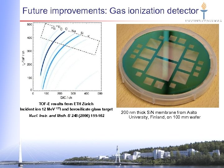 Future improvements: Gas ionization detector 30 m m TOF-E results from ETH Zürich Incident ion 12 Me. V 127 I and borosilicate glass target Nucl. Instr. and Meth. B 248 (2006) 155 -162 200 nm thick Si. N membrane from Aalto University, Finland, on 100 mm wafer
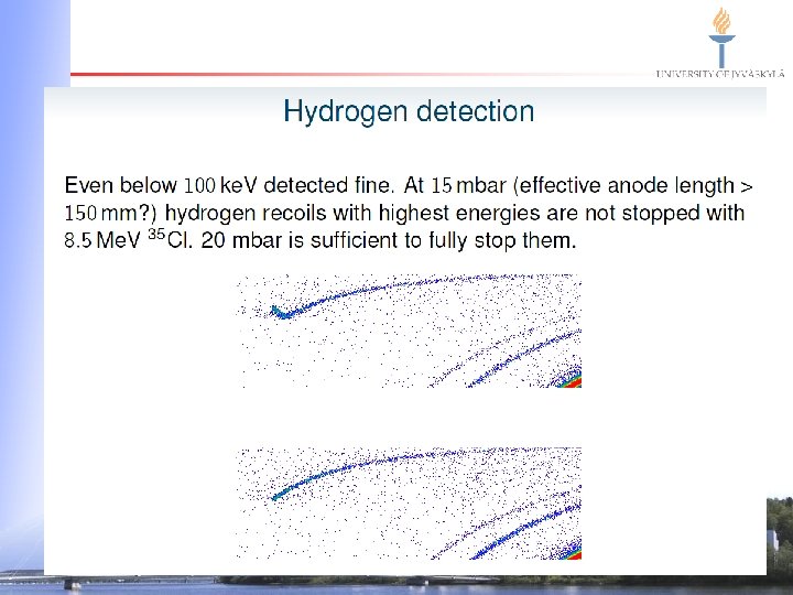
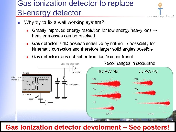 Gas ionization detector to replace Si-energy detector n Why try to fix a well working system? n n n Greatly improved energy resolution for low energy heavy ions → heavier masses can be resolved Gas detector is 1 D position sensitive by nature → possibility for kinematic correction and therefore larger solid angles possible Gas detector does not suffer from ion bombardment Recoil ranges in isobutane 10. 2 Me. V 79 Br 8. 5 Me. V 35 Cl Gas ionization detector develoment – See posters!
