L26 Solid State Physics 1.pptx
- Количество слайдов: 28
 L 26 – Solid State Physics 1 OUTLINE 1. Crystal Structures and Bonding in Solids 2. Band Theory of Solids 3. Electrical Conduction in Metals, Insulators and Semiconductors 1
 1. The Crystal Structure and Bonding in Solids § Condensed matter includes liquids and solids; § The distance between atoms is of the order of the atom size (~ 0. 1 – 0. 5 nm); § X-ray, electron and neutron diffraction are used to determine the inner structure of solids. 2
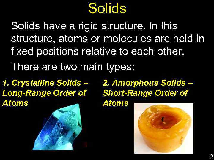 Solids have a rigid structure. In this structure, atoms or molecules are held in fixed positions relative to each other. There are two main types: 1. Crystalline Solids – Long-Range Order of Atoms 2. Amorphous Solids – Short-Range Order of Atoms 3
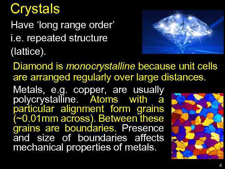 Crystals Have ‘long range order’ i. e. repeated structure (lattice). Diamond is monocrystalline because unit cells are arranged regularly over large distances. Metals, e. g. copper, are usually polycrystalline. Atoms with a particular alignment form grains (~0. 01 mm across). Between these grains are boundaries. Presence and size of boundaries affects mechanical properties of metals. 4
 Crystal lattices and structures § A crystal lattice is a repeating pattern of (mathematical) points called lattice points; § Each atom (or group of atoms) is associated with a lattice point; § Depending on size of atoms and their interactions, solid crystals have different crystallographic structures. 5
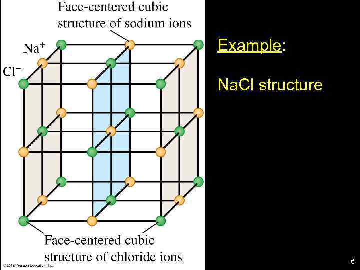 Example: Na. Cl structure 6
 Crystals Vocab Crystalline: Repeating or periodic array over large atomic distances. 3 -D pattern in which each atom is bonded to its nearest neighbors; Crystal structure: the manner in which atoms, ions, or molecules are spatially arranged. Unit cell: small, repeating, entity of the atomic structure. The basic building block of the crystal structure. It defines the entire crystal structure with the atoms positions within. 7
 Studying crystal structures Crystals are generally strong due to covalent or ionic bonds; Regular atomic structures are studied using X-ray diffraction; X-rays have a wavelength of about 10 -10 m, comparable to interatomic spacing; The principles are similar to spectroscopy using a diffraction grating. 8
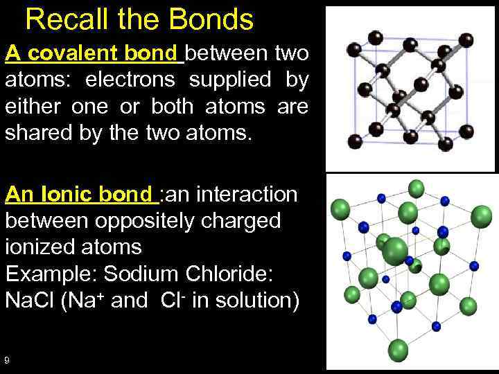 Recall the Bonds A covalent bond between two atoms: electrons supplied by either one or both atoms are shared by the two atoms. An Ionic bond : an interaction between oppositely charged ionized atoms Example: Sodium Chloride: Na. Cl (Na+ and Cl- in solution) 9
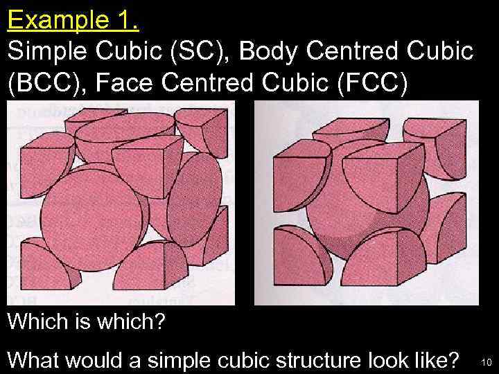 Example 1. Simple Cubic (SC), Body Centred Cubic (BCC), Face Centred Cubic (FCC) Which is which? What would a simple cubic structure look like? 10
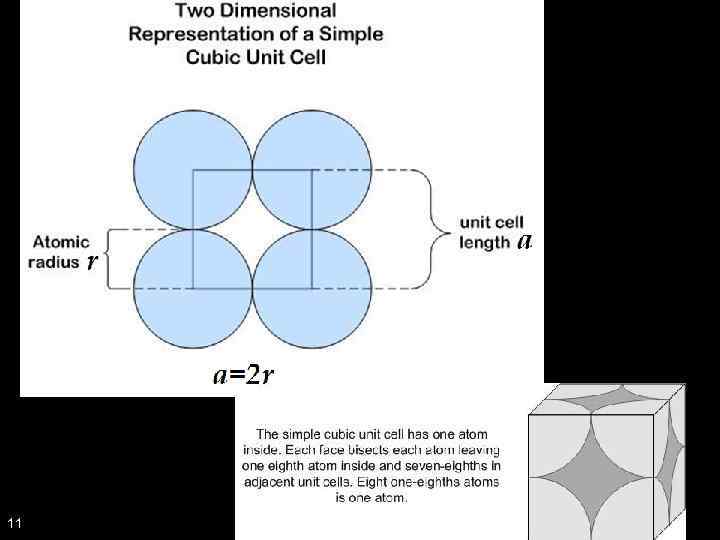 11
11
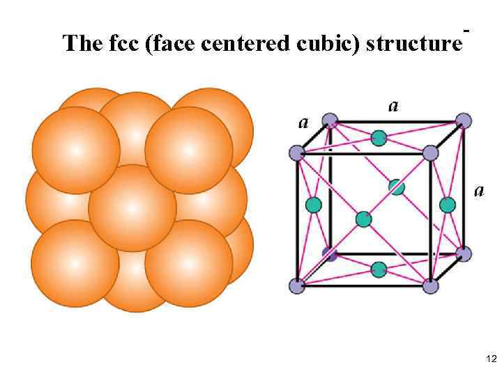 The fcc (face centered cubic) structure - 12
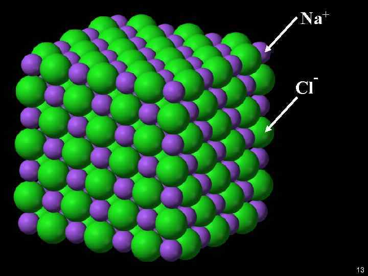 Na+ Cl - 13
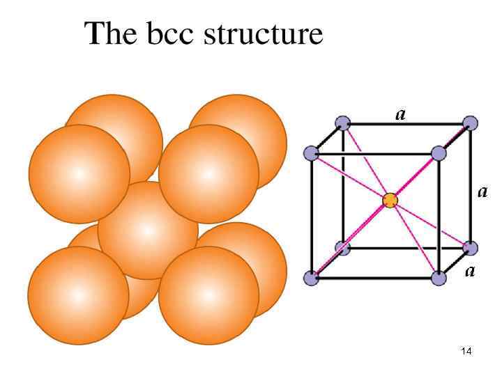 14
14
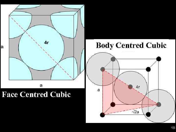 Body Centred Cubic Face Centred Cubic 15
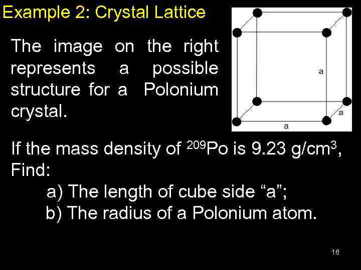 Example 2: Crystal Lattice The image on the right represents a possible structure for a Polonium crystal. If the mass density of 209 Po is 9. 23 g/cm 3, Find: a) The length of cube side “a”; b) The radius of a Polonium atom. 16
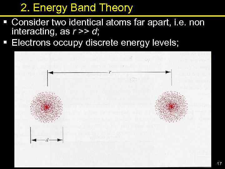 2. Energy Band Theory § Consider two identical atoms far apart, i. e. non interacting, as r >> d; § Electrons occupy discrete energy levels; 17
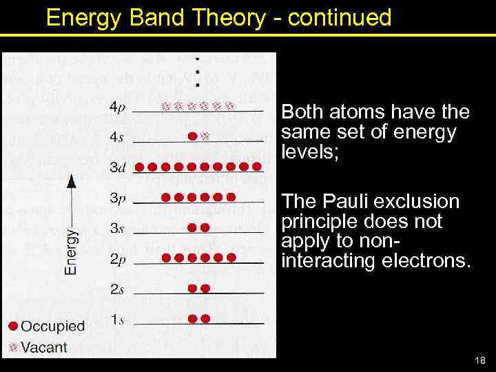 Energy Band Theory - continued Both atoms have the same set of energy levels; The Pauli exclusion principle does not apply to noninteracting electrons. 18
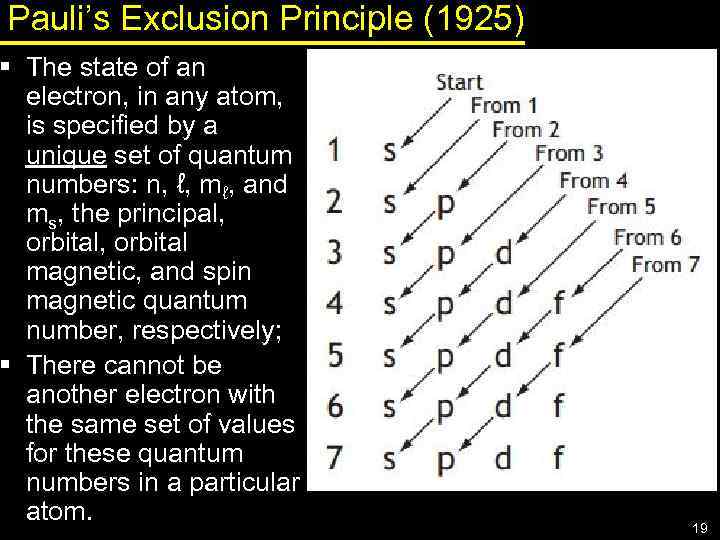 Pauli’s Exclusion Principle (1925) § The state of an electron, in any atom, is specified by a unique set of quantum numbers: n, ℓ, mℓ, and ms, the principal, orbital magnetic, and spin magnetic quantum number, respectively; § There cannot be another electron with the same set of values for these quantum numbers in a particular atom. 19
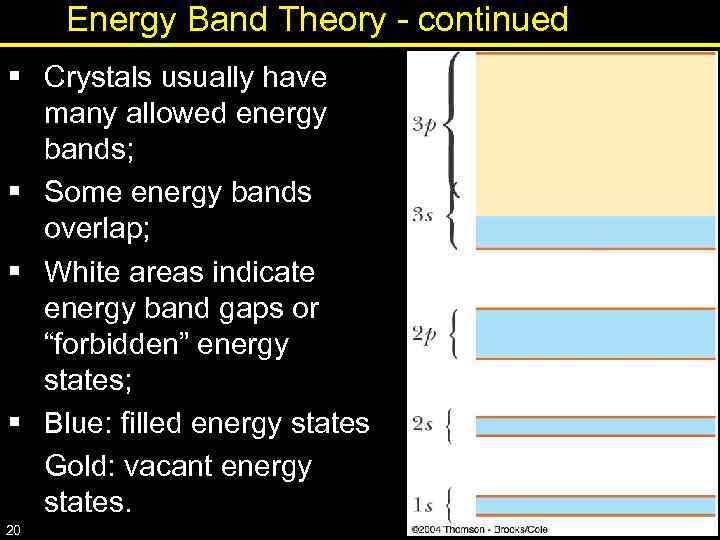 Energy Band Theory - continued § Crystals usually have many allowed energy bands; § Some energy bands overlap; § White areas indicate energy band gaps or “forbidden” energy states; § Blue: filled energy states Gold: vacant energy states. 20
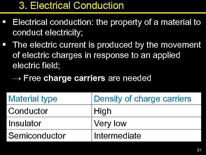 3. Electrical Conduction § Electrical conduction: the property of a material to conduct electricity; § The electric current is produced by the movement of electric charges in response to an applied electric field; → Free charge carriers are needed Material type Conductor Insulator Semiconductor Density of charge carriers High Very low Intermediate 21
 Electrical Conduction - continued § When an external electric field is applied to a conductor, an amount of Kinetic Energy is transferred to charge carriers; § These charge carriers could then jump to Higher energy states if these are available; § The energy band model could be used to explain and estimate the charge carrier density. 22
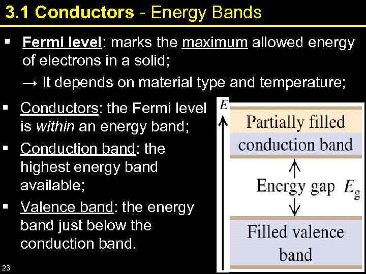 3. 1 Conductors - Energy Bands § Fermi level: marks the maximum allowed energy of electrons in a solid; → It depends on material type and temperature; § Conductors: the Fermi level is within an energy band; § Conduction band: the highest energy band available; § Valence band: the energy band just below the conduction band. 23
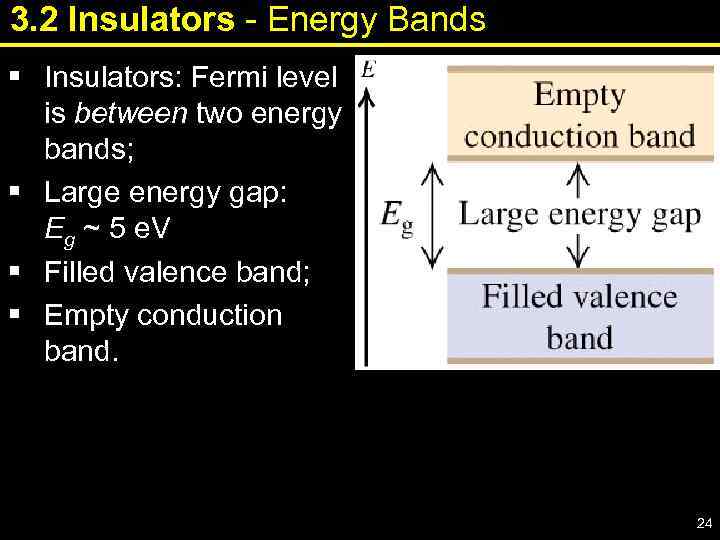 3. 2 Insulators - Energy Bands § Insulators: Fermi level is between two energy bands; § Large energy gap: Eg ~ 5 e. V § Filled valence band; § Empty conduction band. 24
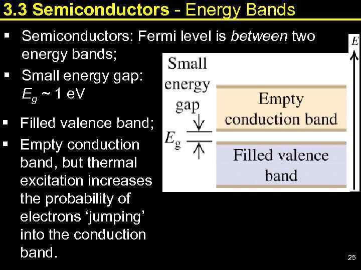 3. 3 Semiconductors - Energy Bands § Semiconductors: Fermi level is between two energy bands; § Small energy gap: Eg ~ 1 e. V § Filled valence band; § Empty conduction band, but thermal excitation increases the probability of electrons ‘jumping’ into the conduction band. 25
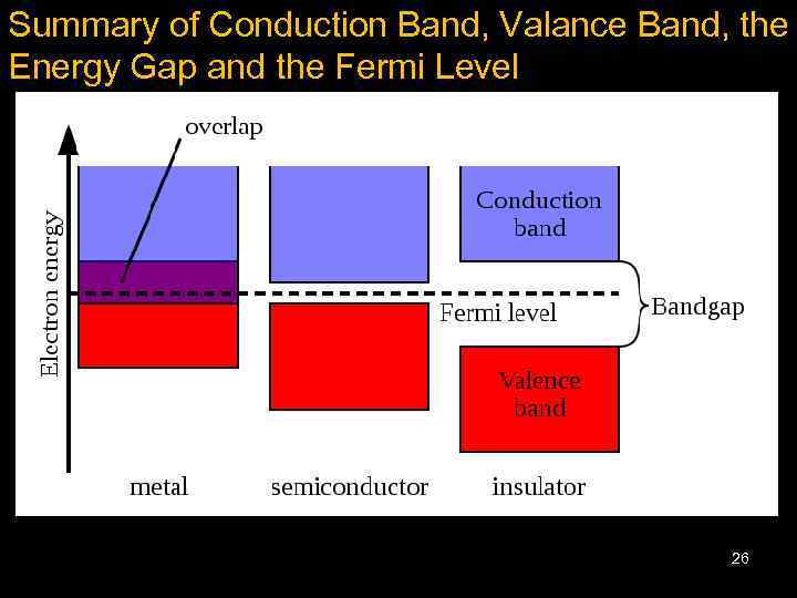 Summary of Conduction Band, Valance Band, the Energy Gap and the Fermi Level 26
 Reading • Adams and Allday Advanced PHYSICS – Chapter 10 Sections: 10. 4, 10. 15 https: //www. youtube. com/watch? v=um-Yimkr. WMM https: //www. youtube. com/watch? v=Icr. Bq. CFLHIY 27
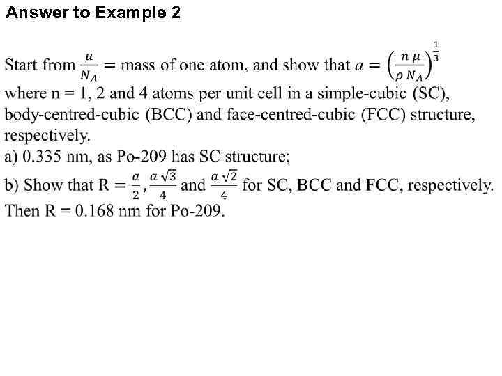 Answer to Example 2


