dceb54b0af2f65bbfa737dcbfbafc71a.ppt
- Количество слайдов: 49
 Knowledge Exchange Towards High-k Dielectrics, CMOS and Solar Cells Simon Rushworth Tyndall National Institute University College Cork Ireland simon. rushworth@tyndall. ie 1
 Outline • Introduction • Field background • FORME project • Knowledge exchange protocols • Atomic Layer Deposition • Results • Applications • Conclusion 2
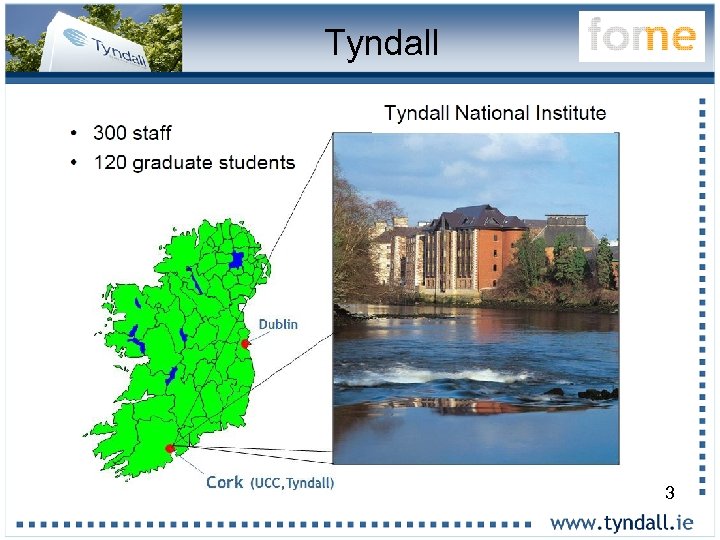 Tyndall 3
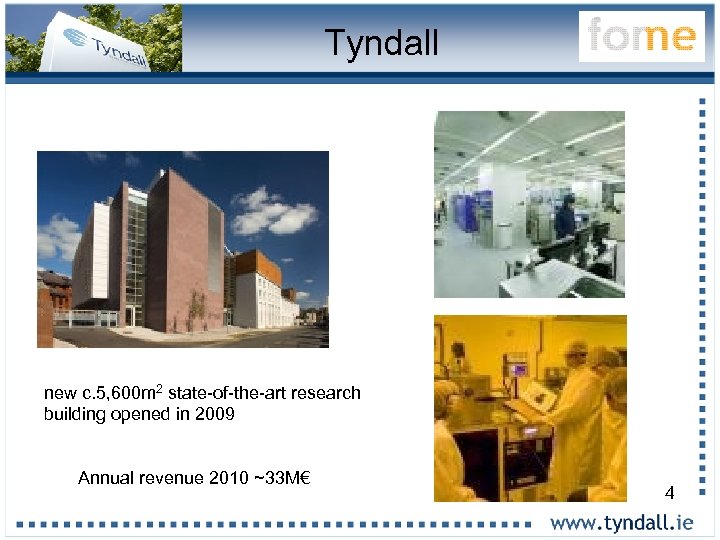 Tyndall new c. 5, 600 m 2 state-of-the-art research building opened in 2009 Annual revenue 2010 ~33 M€ 4
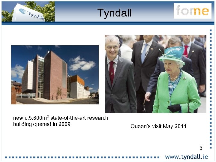 Tyndall new c. 5, 600 m 2 state-of-the-art research building opened in 2009 Queen’s visit May 2011 5
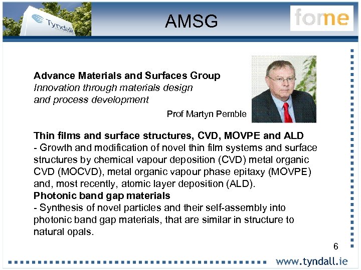 AMSG Advance Materials and Surfaces Group Innovation through materials design and process development Prof Martyn Pemble Thin films and surface structures, CVD, MOVPE and ALD - Growth and modification of novel thin film systems and surface structures by chemical vapour deposition (CVD) metal organic CVD (MOCVD), metal organic vapour phase epitaxy (MOVPE) and, most recently, atomic layer deposition (ALD). Photonic band gap materials - Synthesis of novel particles and their self-assembly into photonic band gap materials, that are similar in structure to natural opals. 6
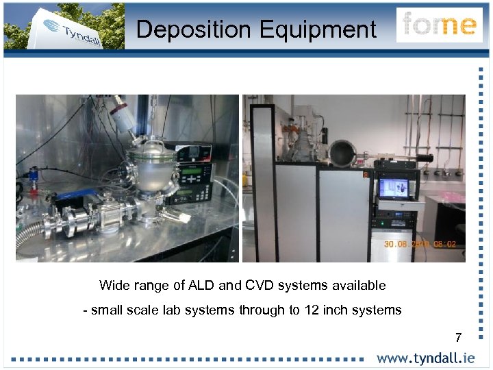 Deposition Equipment Wide range of ALD and CVD systems available - small scale lab systems through to 12 inch systems 7
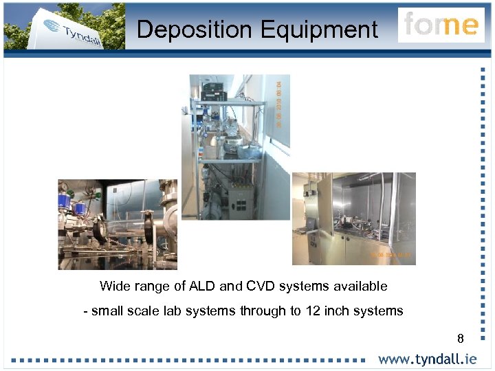 Deposition Equipment Wide range of ALD and CVD systems available - small scale lab systems through to 12 inch systems 8
 Outline • Introduction • Field background • FORME project • Knowledge exchange protocols • Atomic Layer Deposition • Results • Applications • Conclusion 9
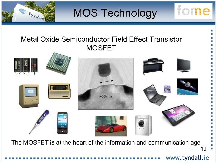 MOS Technology Metal Oxide Semiconductor Field Effect Transistor MOSFET The MOSFET is at the heart of the information and communication age 10
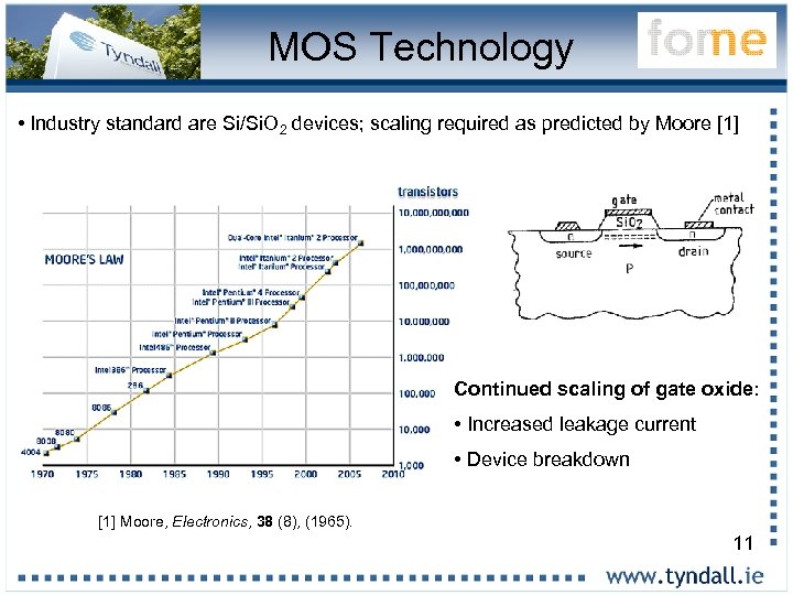 MOS Technology • Industry standard are Si/Si. O 2 devices; scaling required as predicted by Moore [1] Continued scaling of gate oxide: • Increased leakage current • Device breakdown [1] Moore, Electronics, 38 (8), (1965). 11
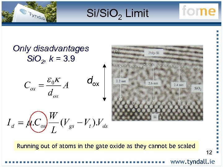 Si/Si. O 2 Limit Only disadvantages Si. O 2, k = 3. 9 Al dox As, P B Running out of atoms in the gate oxide as they cannot be scaled 12
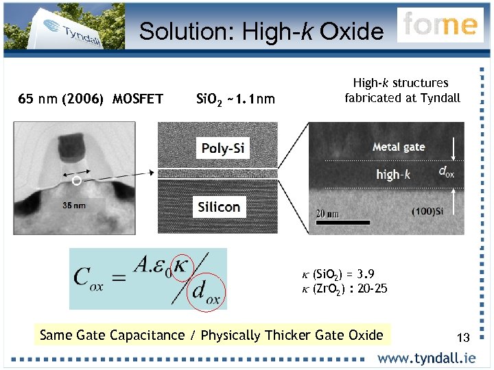 Solution: High-k Oxide 65 nm (2006) MOSFET Si. O 2 ~1. 1 nm High-k structures fabricated at Tyndall k (Si. O 2) = 3. 9 k (Zr. O 2) : 20 -25 Same Gate Capacitance / Physically Thicker Gate Oxide 13
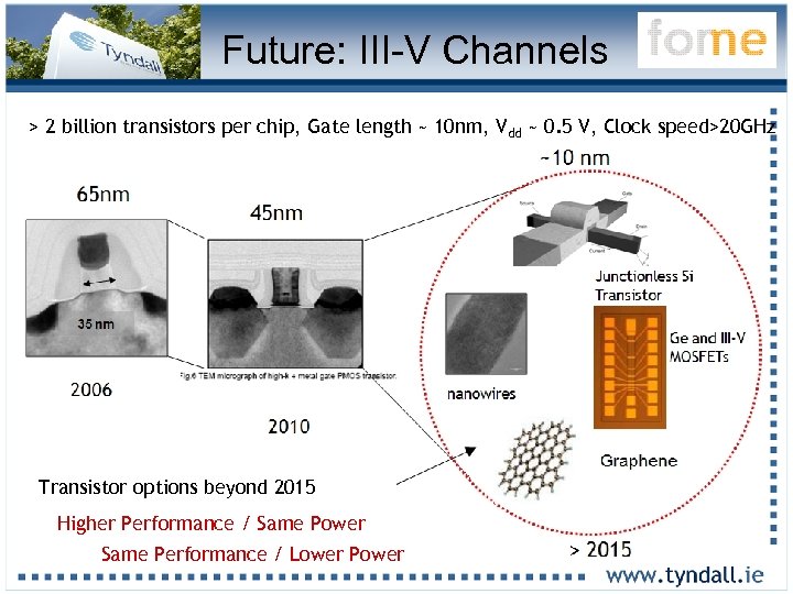 Future: III-V Channels > 2 billion transistors per chip, Gate length ~ 10 nm, Vdd ~ 0. 5 V, Clock speed>20 GHz Transistor options beyond 2015 Higher Performance / Same Power Same Performance / Lower Power 14
 Outline • Introduction • Field background • FORME project • Knowledge exchange protocols • Atomic Layer Deposition • Results • Applications • Conclusion 15
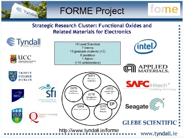 FORME Project Strategic Research Cluster: Functional Oxides and Related Materials for Electronics 16 Lead Scientists 7 interns 18 graduate students (+2) 6 postdocs 1 Admin (+18 collaborators) http: //www. tyndall. ie/forme 16
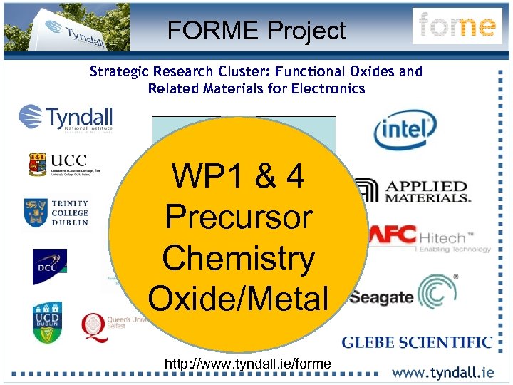 FORME Project Strategic Research Cluster: Functional Oxides and Related Materials for Electronics 16 Lead Scientists 7 interns 18 graduate students (+2) 6 postdocs 1 Admin (+18 collaborators) WP 1 & 4 Precursor Chemistry Oxide/Metal http: //www. tyndall. ie/forme 17
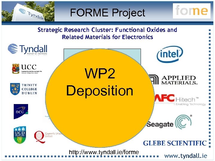 FORME Project Strategic Research Cluster: Functional Oxides and Related Materials for Electronics 16 Lead Scientists 7 interns 18 graduate students (+2) 6 postdocs 1 Admin (+18 collaborators) WP 2 Deposition http: //www. tyndall. ie/forme 18
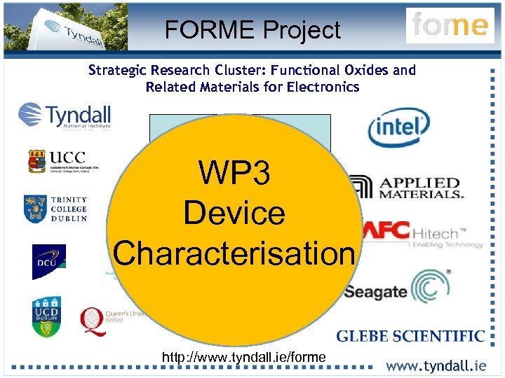 FORME Project Strategic Research Cluster: Functional Oxides and Related Materials for Electronics 16 Lead Scientists 7 interns 18 graduate students (+2) 6 postdocs 1 Admin (+18 collaborators) WP 3 Device Characterisation http: //www. tyndall. ie/forme 19
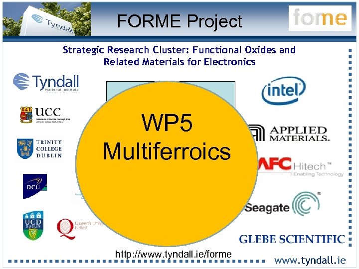 FORME Project Strategic Research Cluster: Functional Oxides and Related Materials for Electronics 16 Lead Scientists 7 interns 18 graduate students (+2) 6 postdocs 1 Admin (+18 collaborators) WP 5 Multiferroics http: //www. tyndall. ie/forme 20
 FORME Project Strategic Research Cluster: Functional Oxides and Related Materials for Electronics 16 Lead Scientists 7 interns 18 graduate students (+2) 6 postdocs 1 Admin (+18 collaborators) WP 6 Management Exploitation http: //www. tyndall. ie/forme 21
 FORME Project Strategic Research Cluster: Functional Oxides and Related Materials for Electronics 16 Lead Scientists 7 interns 18 graduate students (+2) 6 postdocs 1 Admin (+18 collaborators) EP Photovoltaics http: //www. tyndall. ie/forme 22
 Outline • Introduction • Field background • FORME project • Knowledge exchange protocols • Atomic Layer Deposition • Results • Applications • Conclusion 23
 Knowledge Exchange describes the processes, mechanisms, networks and relationships that enable knowledge derived from research activity to move between organisations. The term is applied to the sharing of knowledge that has potential impact on innovation, and to change, transform, enhance or generate new or improved professional practices, policies, technologies, products, services and public perceptions. ie Talking to one another to spread the word and advance state of the art 24
 Commercialisation describes the process by which the outcomes of research activity are brought to the market place through the development of new products, processes, services or technologies. The process involves the identification of research which has potential commercial interest and the designing of strategies for how to exploit this research. This will include the protecting and managing of the rights to intellectual property. Strategies can include the creation of licensing agreements or joint ventures, partnerships, or spin-out companies. ie Talking to one another to deliver new products to make money 25
 Disconnect The Knowledge Inventor is usually a scientist working in a highly specific area and interested in moving forward state of the art The Knowledge Exploiter is usually a business man working in a different area and interested in growing the company revenue These two entities, with different outlooks and desires, require somebody to bring them together. More Universities and Companies are establishing Technology Transfer Offices to address the disconnect At the onset of the project a collaboration agreement was implemented to establish protocols to try to address this issue 26
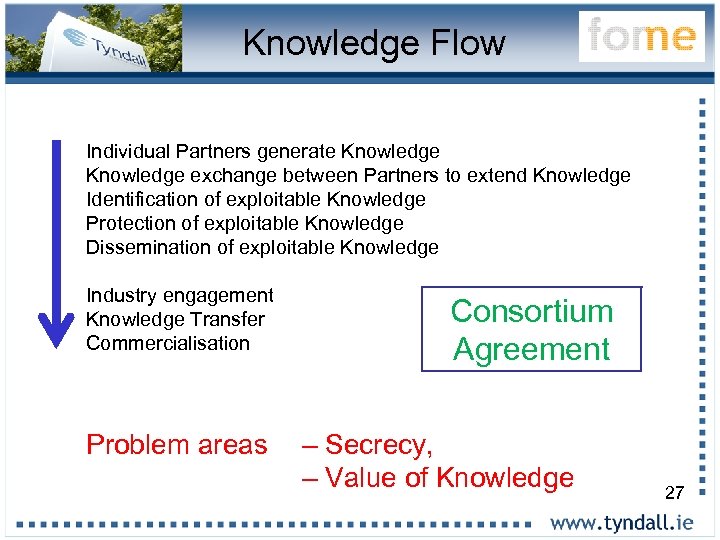 Knowledge Flow Individual Partners generate Knowledge exchange between Partners to extend Knowledge Identification of exploitable Knowledge Protection of exploitable Knowledge Dissemination of exploitable Knowledge Industry engagement Knowledge Transfer Commercialisation Problem areas Consortium Agreement – Secrecy, – Value of Knowledge 27
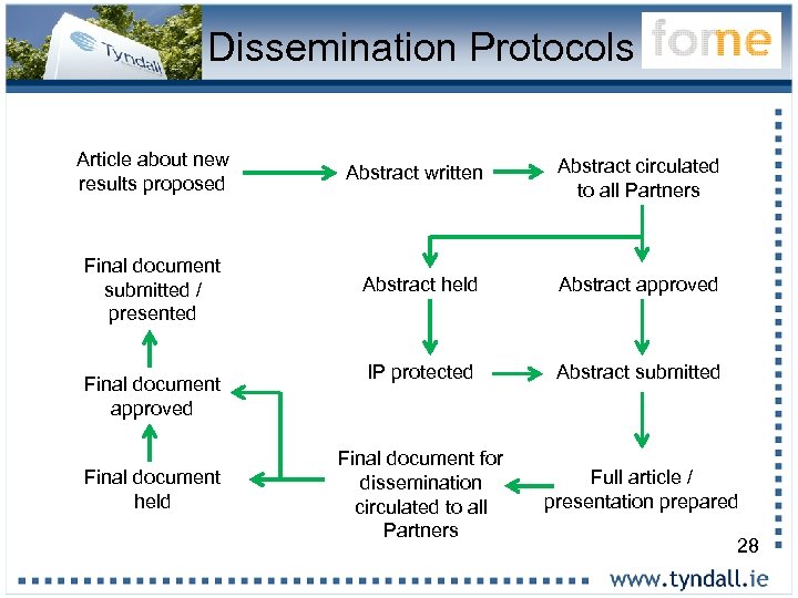 Dissemination Protocols Article about new results proposed Final document submitted / presented Final document approved Final document held Abstract written Abstract circulated to all Partners Abstract held Abstract approved IP protected Abstract submitted Final document for dissemination circulated to all Partners Full article / presentation prepared 28
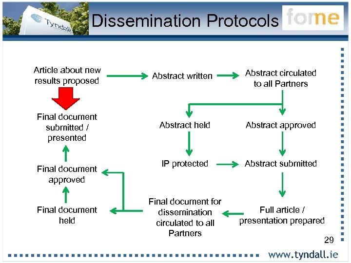 Dissemination Protocols Article about new results proposed Final document submitted / presented Final document approved Final document held Abstract written Abstract circulated to all Partners Abstract held Abstract approved IP protected Abstract submitted Final document for dissemination circulated to all Partners Full article / presentation prepared 29
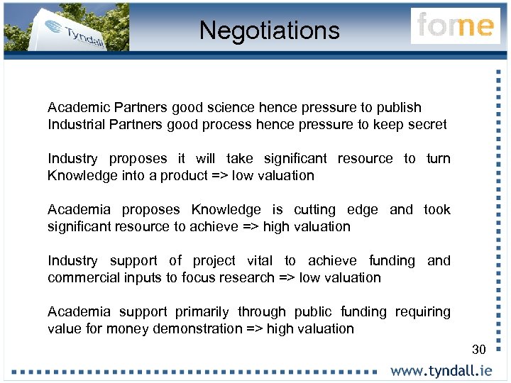 Negotiations Academic Partners good science hence pressure to publish Industrial Partners good process hence pressure to keep secret Industry proposes it will take significant resource to turn Knowledge into a product => low valuation Academia proposes Knowledge is cutting edge and took significant resource to achieve => high valuation Industry support of project vital to achieve funding and commercial inputs to focus research => low valuation Academia support primarily through public funding requiring value for money demonstration => high valuation 30
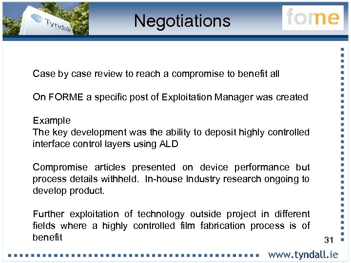 Negotiations Case by case review to reach a compromise to benefit all On FORME a specific post of Exploitation Manager was created Example The key development was the ability to deposit highly controlled interface control layers using ALD Compromise articles presented on device performance but process details withheld. In-house Industry research ongoing to develop product. Further exploitation of technology outside project in different fields where a highly controlled film fabrication process is of benefit 31
 Outline • Introduction • Field background • FORME project • Knowledge exchange protocols • Atomic Layer Deposition • Results • Applications • Conclusion 32
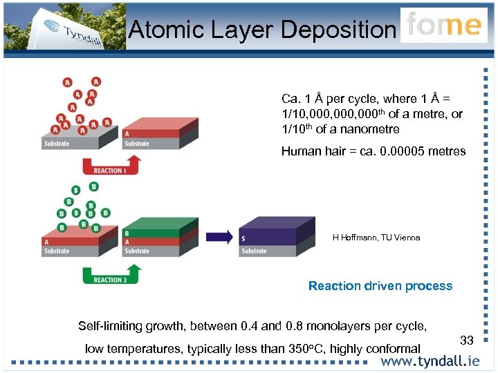 Atomic Layer Deposition Ca. 1 Å per cycle, where 1 Å = 1/10, 000, 000 th of a metre, or 1/10 th of a nanometre Human hair = ca. 0. 00005 metres H Hoffmann, TU Vienna Reaction driven process Self-limiting growth, between 0. 4 and 0. 8 monolayers per cycle, low temperatures, typically less than 350 o. C, highly conformal 33
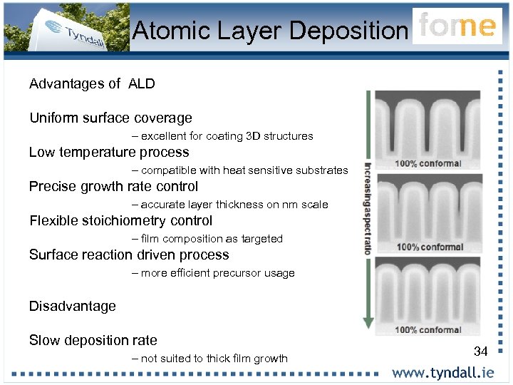 Atomic Layer Deposition Advantages of ALD Uniform surface coverage – excellent for coating 3 D structures Low temperature process – compatible with heat sensitive substrates Precise growth rate control – accurate layer thickness on nm scale Flexible stoichiometry control – film composition as targeted Surface reaction driven process – more efficient precursor usage Disadvantage Slow deposition rate – not suited to thick film growth 34
 Material Systems Oxides Al 2 O 3, Ti. O 2, Zn. O, Zr. O 2, Hf. O 2, Mg. O, Ca. O, Ga 2 O 3 Nitrides Ti. N, Ta. N Metals Ir, Ru, Co, Cu, others Current areas of interest Interface control and surface modification processes new chemistries 35
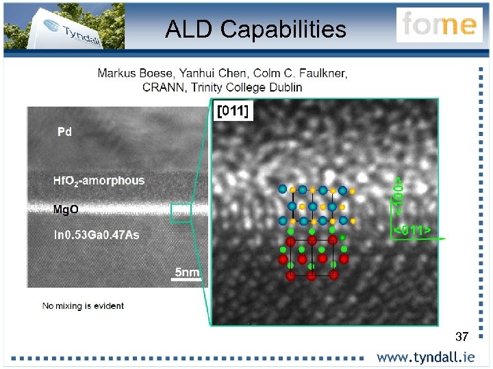
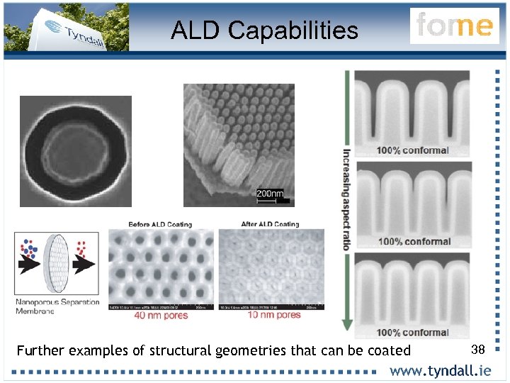
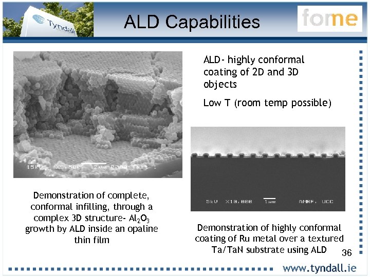 ALD Capabilities ALD- highly conformal coating of 2 D and 3 D objects Low T (room temp possible) Demonstration of complete, conformal infilling, through a complex 3 D structure- Al 2 O 3 growth by ALD inside an opaline thin film Demonstration of highly conformal coating of Ru metal over a textured Ta/Ta. N substrate using ALD 36
 ALD Capabilities 37
 ALD Capabilities Further examples of structural geometries that can be coated 38
 Target Application High-k on III-V MOSFETs 39
 Target Application High-k on III-V MOSFETs 40
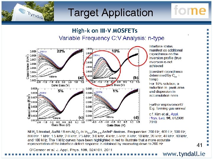 Target Application High-k on III-V MOSFETs 41
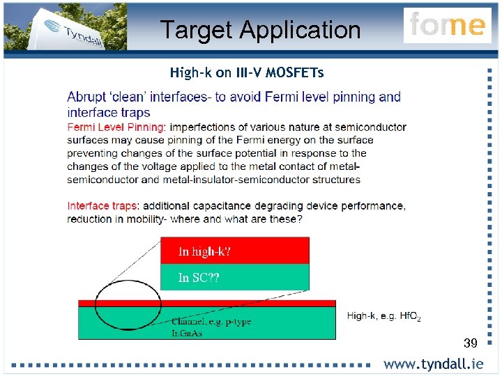
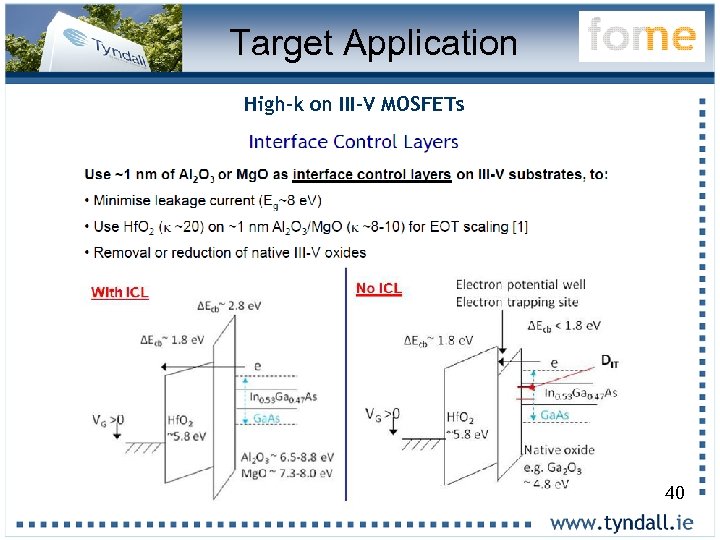
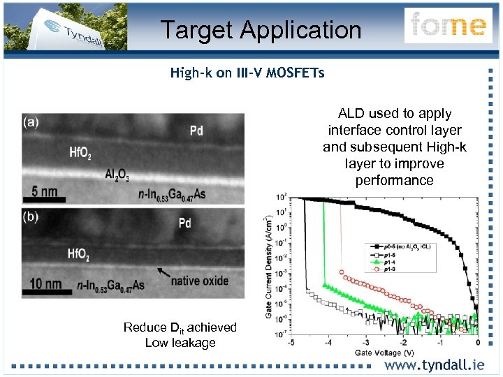 Target Application High-k on III-V MOSFETs ALD used to apply interface control layer and subsequent High-k layer to improve performance Reduce Dit achieved Low leakage 42
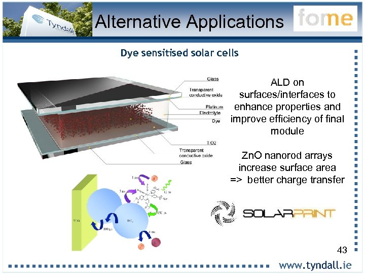 Alternative Applications Dye sensitised solar cells ALD on surfaces/interfaces to enhance properties and improve efficiency of final module Zn. O nanorod arrays increase surface area => better charge transfer 43
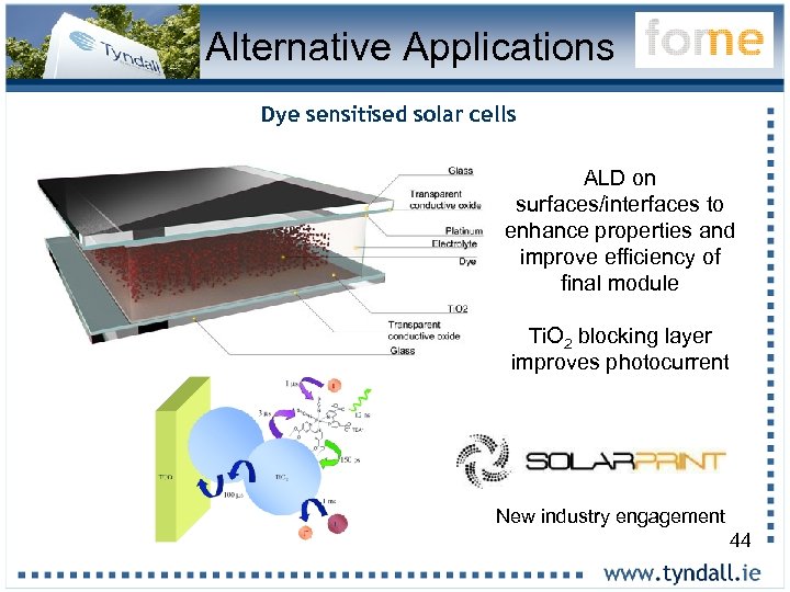 Alternative Applications Dye sensitised solar cells ALD on surfaces/interfaces to enhance properties and improve efficiency of final module Ti. O 2 blocking layer improves photocurrent New industry engagement 44
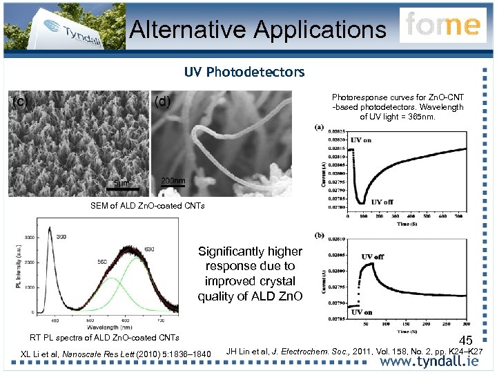 Alternative Applications UV Photodetectors Photoresponse curves for Zn. O-CNT -based photodetectors. Wavelength of UV light = 365 nm. SEM of ALD Zn. O-coated CNTs Significantly higher response due to improved crystal quality of ALD Zn. O RT PL spectra of ALD Zn. O-coated CNTs XL Li et al, Nanoscale Res Lett (2010) 5: 1836– 1840 45 JH Lin et al, J. Electrochem. Soc. , 2011, Vol. 158, No. 2, pp. K 24–K 27
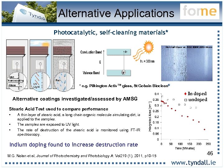 Alternative Applications Photocatalytic, self-cleaning materials* * e. g. Pilkington Activ TM glass, St Gobain Bioclean® Alternative coatings investigated/assessed by AMSG ♦ In doped □ undoped Stearic Acid Test used to compare performance • • • A thin layer of stearic acid, a long chain organic molecule simulating dirt, is applied to the samples. The samples are exposed to UV light. The rate of destruction of the stearic acid is monitored using FT-IR spectroscopy. Indium doping found to increase destruction rate M. G. Nolan et al, Journal of Photochemistry and Photobiology A: Vol 219 (1), 2011, p 10 -15 46
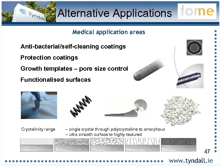 Alternative Applications Medical application areas Anti-bacterial/self-cleaning coatings Protection coatings Growth templates – pore size control Functionalised surfaces Crystallinity range – single crystal through polycrystalline to amorphous – ultra smooth surface to highly textured 47
 Conclusions Technically advanced Atomic Layer Deposition processes have been developed to allow the controlled uniform deposition of nm thick metal oxide films capable of enhancing surface functionality Technology development is a partnership - effective Knowledge Exchange is critical Commercialisation is a partnership - effective Knowledge Exchange and Transfer is critical Academic and Industry engagement is good for all 48
 Thank you for your attention PS. Any parties interested in collaboration please contact me simon. rushworth@tyndall. ie http: //www. tyndall. ie/forme 49


