b07396b1da8ed6d0f82b9e33fc9778b4.ppt
- Количество слайдов: 123

IR Sensor System for Aquatic Neurobehavioral Research – Presentation 2 Team 4 October 25 th, 2006 1
Team 4: Members n Jeff Mueller: LPI – BSEE n Chad Due: LMM – BSEE n Jon Reisner: LPM – BSEE n Aleks Plavsic: LSD – BSEE n John Schwittay: LRN – BSEE 2

Project Proposal n This product will be designed to test the effects of positive reinforcement in a controlled habitat for fish Automated experiments and data collection ¨ Test different health concerns in fish ¨ n n Project will be the first attempt to collect data for aquatic neurobehavioral studies No known products are currently on the market Device will be used at Great Lakes Institute, Milwaukee, WI Product could be modified to assist similar water & marine studies 3
Risks and Problem Areas n n n Infrared beams’ transmission through water and potential damage to specimen’s (fish) tissue (i. e. eyes). Potential long lead time for IR transmitters (laser diodes), IR receivers, display, and stepper motors. Possible need for placement of IR sensing block inside the fish tank Possible prototyping issue with the fish tank and water Potential need for Lab. VIEW (expensive) Advantages of Project for Team #4: Previous research and experience in optics ¨ Prior microprocessor design and buildup ¨ Knowledge of control devices ¨ 4
US Patents n US 6, 627, 892 - Infrared detector packaged with improved antireflection element; September 30, 2003 n US 6, 082, 299 - Automatic fish feeder; July 4, 2000 n US 6, 433, 684 - Device for detecting and signaling or indicating status as regards contents in a container, and in particular a letterbox; August 13, 2002 5

Estimation-Reconciliation Summary n n n Total Manpower Estimated: 762 hours Total Manpower Anticipated: 1100 hours Total Material $ Estimated: $535 Total Material $ Anticipated: $1000 Manpower Allocation: ¨ System Design Tasks ¨ Detailed Design Tasks ¨ Verification Tasks ¨ Documentation Tasks 25% 35% 10% 30 % 6
System Level Requirements n Standard Requirements Power n One AC Energy Source n Min Oper. Voltage Range: 100 -264 V n Frequency Range: 47 -63 Hz n Max Total Power (AC): 84 W ¨ Environmental n Min. Oper. Temp. Range: 10 – 40°C n Min. Storage Temp. Range: -10 – 60°C n Min. Oper. Humidity Range: 0 – 80%Rh n Min. Storage Humidity Range: 0 – 100%Rh n Min. Oper. Altitude Range: 0 – 2000 m n Min. Storage/Shipping Altitude Range: 0 -1500 m n Max Storage Duration: 10 yrs. ¨ 7
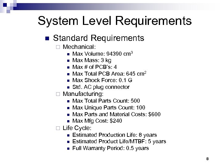
System Level Requirements n Standard Requirements ¨ Mechanical: n n n ¨ Manufacturing: n n ¨ Max Volume: 94390 cm 3 Max Mass: 3 kg Max # of PCB’s: 4 Max Total PCB Area: 645 cm 2 Max Shock Force: 0. 1 G Std. AC plug connector Max Total Parts Count: 500 Max Unique Parts Count: 100 Max Parts and Material Costs: $600 Max Mfg Cost: $240 Life Cycle: n n n Estimated Production Life: 8 years Estimated Product Life/MTBF: 5 years Full Warranty Period: 0. 5 years 8
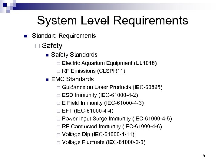
System Level Requirements n Standard Requirements ¨ Safety n Safety Standards ¨ ¨ n Electric Aquarium Equipment (UL 1018) RF Emissions (CLSPR 11) EMC Standards ¨ ¨ ¨ ¨ Guidance on Laser Products (IEC-60825) ESD Immunity (IEC-61000 -4 -2) E Field Immunity (IEC-61000 -4 -3) EFT (IEC-61000 -4 -4) Power Input Surge Immunity (IEC-61000 -4 -5) RF Conducted Immunity (IEC-61000 -4 -6) Voltage Dip (IEC-61000 -4 -11) Voltage Fluctuate (IEC-61000 -3 -3) 9
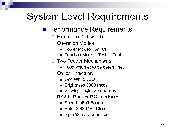
System Level Requirements n Performance Requirements External on/off switch ¨ Operation Modes: ¨ n n ¨ Two Feeder Mechanisms: n ¨ Food volume: to be determined Optical Indicator: n n n ¨ Power Modes: On, Off Function Modes: Test 1, Test 2 One White LED Brightness: 6000 mcds Viewing angle: 20 degrees RS 232 Port for PC interface: n n n Speed: 9600 Bauds Rate: 3. 68 MHz Clock 9 pin Serial Connector 10
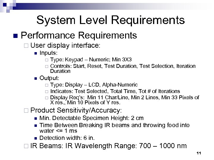
System Level Requirements n Performance Requirements ¨ User display interface: n Inputs: Type: Keypad – Numeric; Min 3 X 3 ¨ Controls: Start, Reset, Test Duration, Test Selection, Iteration Duration Output: ¨ Type: Display – LCD, Alpha-Numeric ¨ Indicates: Test Selected, Total Time, Tot # of Iterations ¨ Display Req’s: Min 11 Char/Line, Min 2 Lines, Min 33 Pixels of X res. , Min 10 Pixels of Y res. ¨ n ¨ Product Sensitivity/Accuracy: n Min. Detectable Specimen Height: 2 cm n Time Between Breaking IR beams and throwing food into water <= 1 ms n Detection width: 6 in. ¨ IR Beams: IR Wavelength Range: 700 – 1000 nm 11
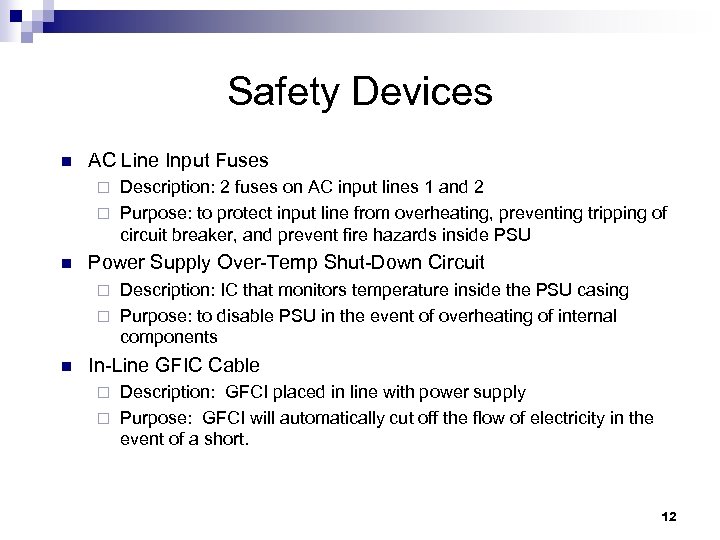
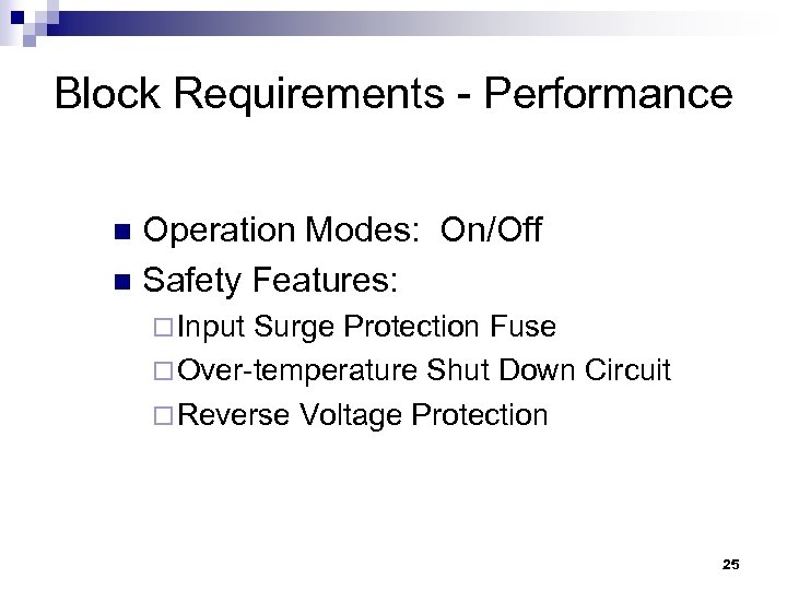
Safety Devices n AC Line Input Fuses Description: 2 fuses on AC input lines 1 and 2 ¨ Purpose: to protect input line from overheating, preventing tripping of circuit breaker, and prevent fire hazards inside PSU ¨ n Power Supply Over-Temp Shut-Down Circuit Description: IC that monitors temperature inside the PSU casing ¨ Purpose: to disable PSU in the event of overheating of internal components ¨ n In-Line GFIC Cable Description: GFCI placed in line with power supply ¨ Purpose: GFCI will automatically cut off the flow of electricity in the event of a short. ¨ 12
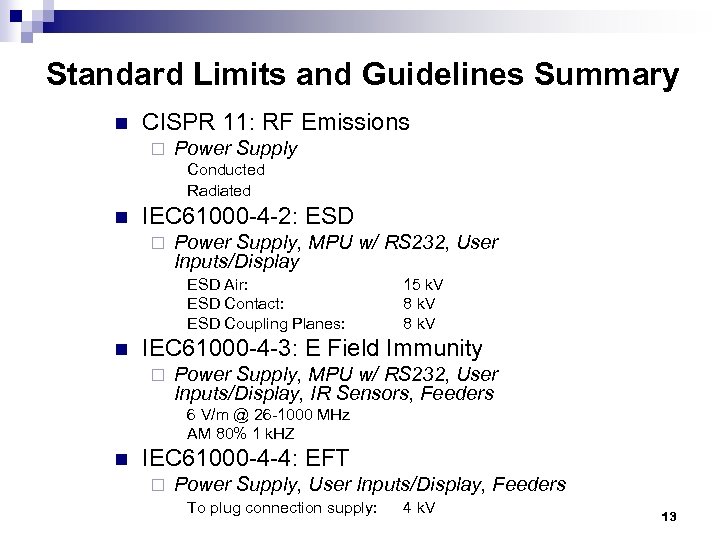
Standard Limits and Guidelines Summary n CISPR 11: RF Emissions ¨ Power Supply Conducted Radiated n IEC 61000 -4 -2: ESD ¨ Power Supply, MPU w/ RS 232, User Inputs/Display ESD Air: ESD Contact: ESD Coupling Planes: n 15 k. V 8 k. V IEC 61000 -4 -3: E Field Immunity ¨ Power Supply, MPU w/ RS 232, User Inputs/Display, IR Sensors, Feeders 6 V/m @ 26 -1000 MHz AM 80% 1 k. HZ n IEC 61000 -4 -4: EFT ¨ Power Supply, User Inputs/Display, Feeders To plug connection supply: 4 k. V 13
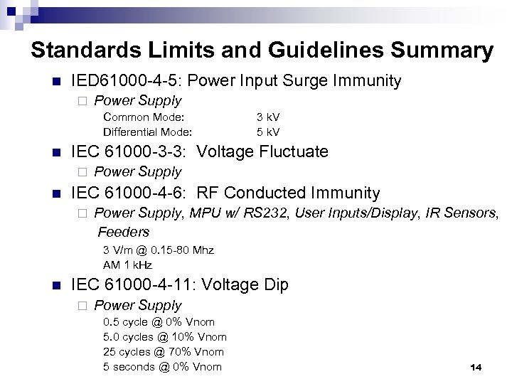
Standards Limits and Guidelines Summary n IED 61000 -4 -5: Power Input Surge Immunity ¨ Power Supply Common Mode: Differential Mode: n IEC 61000 -3 -3: Voltage Fluctuate ¨ n 3 k. V 5 k. V Power Supply IEC 61000 -4 -6: RF Conducted Immunity ¨ Power Supply, MPU w/ RS 232, User Inputs/Display, IR Sensors, Feeders 3 V/m @ 0. 15 -80 Mhz AM 1 k. Hz n IEC 61000 -4 -11: Voltage Dip ¨ Power Supply 0. 5 cycle @ 0% Vnom 5. 0 cycles @ 10% Vnom 25 cycles @ 70% Vnom 5 seconds @ 0% Vnom 14
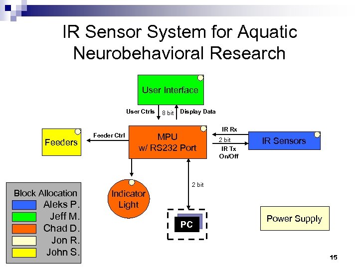
IR Sensor System for Aquatic Neurobehavioral Research User Interface User Ctrls Feeders Block Allocation Aleks P. Jeff M. Chad D. Jon R. John S. Feeder Ctrl 8 bit Display Data MPU w/ RS 232 Port IR Rx 2 bit IR Tx On/Off IR Sensors 2 bit Indicator Light PC Power Supply 15
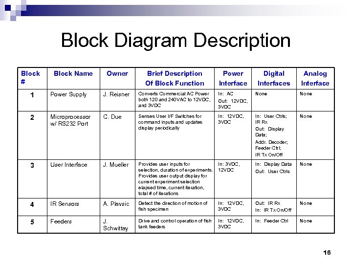
Block Diagram Description Block # Block Name Owner Brief Description Of Block Function Power Interface Digital Interfaces Analog Interface 1 Power Supply J. Reisner Converts Commercial AC Power both 120 and 240 VAC to 12 VDC, and 3 VDC In: AC Out: 12 VDC, 3 VDC None 2 Microprocessor w/ RS 232 Port C. Due Senses User I/F Switches for command inputs and updates display periodically In: 12 VDC, 3 VDC In: User Ctrls; IR Rx Out: Display Data; Addr. Decoder; Feeder Ctrl; IR Tx On/Off None 3 User Interface J. Mueller Provides user inputs for In: 3 VDC, selection, duration of experiments. 12 VDC Provides user output display for current experiment selection elapsed time, current iteration, total # of iterations In: Display Data Out: User Ctrls None 4 IR Sensors A. Plavsic Detect the direction of motion of fish specimen In: 12 VDC, 3 VDC Out: IR Rx In: IR Tx On/Off None 5 Feeders J. Schwittay Drive and control operation of fish tank feeders In: 12 VDC, 3 VDC In: Feeder Ctrl None 16
High Level Project Plan 17
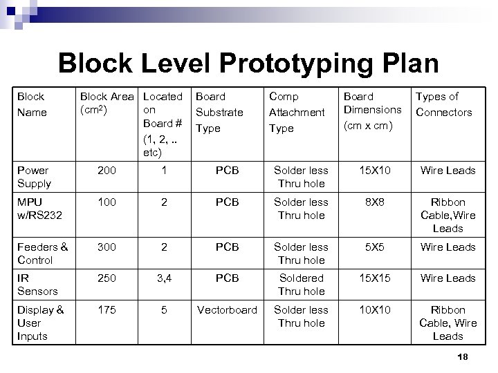
Block Level Prototyping Plan Block Name Block Area Located Board (cm 2) on Substrate Board # Type (1, 2, . . etc) Comp Attachment Type Board Dimensions (cm x cm) Types of Connectors Power Supply 200 1 PCB Solder less Thru hole 15 X 10 Wire Leads MPU w/RS 232 100 2 PCB Solder less Thru hole 8 X 8 Ribbon Cable, Wire Leads Feeders & Control 300 2 PCB Solder less Thru hole 5 X 5 Wire Leads IR Sensors 250 3, 4 PCB Soldered Thru hole 15 X 15 Wire Leads Display & User Inputs 175 5 Vectorboard Solder less Thru hole 10 X 10 Ribbon Cable, Wire Leads 18

Power Supply Team 4 Jon Reisner 19
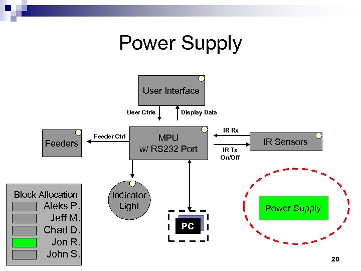
Power Supply User Interface User Ctrls Feeders Block Allocation Aleks P. Jeff M. Chad D. Jon R. John S. Feeder Ctrl Display Data MPU w/ RS 232 Port Indicator Light IR Rx IR Tx On/Off IR Sensors Power Supply PC 20
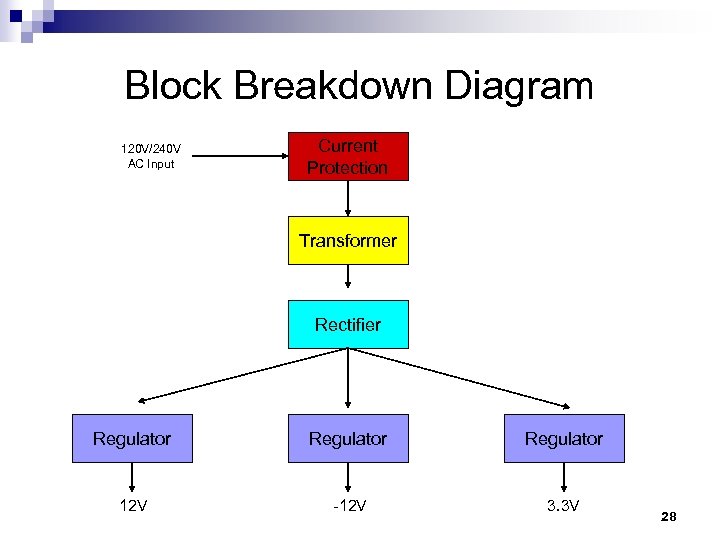
Block Description and Purpose n Description: ¨ n Takes in AC voltage and outputs regulated DC voltages Purpose: Delivers voltage and current as needed by other blocks ¨ Protects other blocks by preventing surges ¨ 21
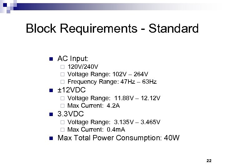
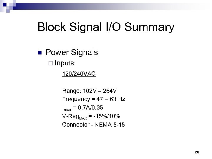
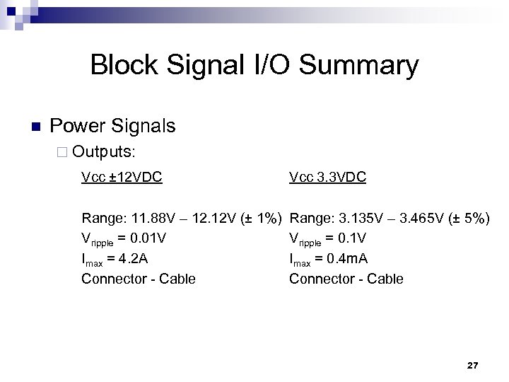
Block Requirements - Standard n AC Input: ¨ ¨ ¨ n ± 12 VDC ¨ ¨ n Voltage Range: 11. 88 V – 12. 12 V Max Current: 4. 2 A 3. 3 VDC ¨ ¨ n 120 V/240 V Voltage Range: 102 V – 264 V Frequency Range: 47 Hz – 63 Hz Voltage Range: 3. 135 V – 3. 465 V Max Current: 0. 4 m. A Max Total Power Consumption: 40 W 22
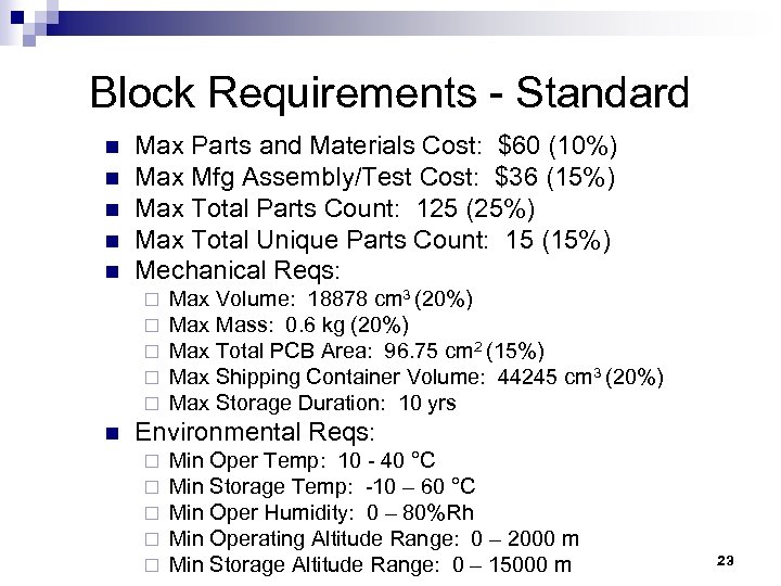
Block Requirements - Standard n n n Max Parts and Materials Cost: $60 (10%) Max Mfg Assembly/Test Cost: $36 (15%) Max Total Parts Count: 125 (25%) Max Total Unique Parts Count: 15 (15%) Mechanical Reqs: ¨ ¨ ¨ n Max Volume: 18878 cm 3 (20%) Max Mass: 0. 6 kg (20%) Max Total PCB Area: 96. 75 cm 2 (15%) Max Shipping Container Volume: 44245 cm 3 (20%) Max Storage Duration: 10 yrs Environmental Reqs: ¨ ¨ ¨ Min Oper Temp: 10 - 40 °C Min Storage Temp: -10 – 60 °C Min Oper Humidity: 0 – 80%Rh Min Operating Altitude Range: 0 – 2000 m Min Storage Altitude Range: 0 – 15000 m 23
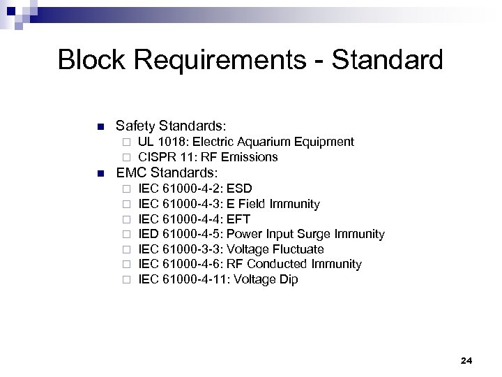
Block Requirements - Standard n Safety Standards: ¨ ¨ n UL 1018: Electric Aquarium Equipment CISPR 11: RF Emissions EMC Standards: ¨ ¨ ¨ ¨ IEC 61000 -4 -2: ESD IEC 61000 -4 -3: E Field Immunity IEC 61000 -4 -4: EFT IED 61000 -4 -5: Power Input Surge Immunity IEC 61000 -3 -3: Voltage Fluctuate IEC 61000 -4 -6: RF Conducted Immunity IEC 61000 -4 -11: Voltage Dip 24
Block Requirements - Performance Operation Modes: On/Off n Safety Features: n ¨ Input Surge Protection Fuse ¨ Over-temperature Shut Down Circuit ¨ Reverse Voltage Protection 25
Block Signal I/O Summary n Power Signals ¨ Inputs: 120/240 VAC Range: 102 V – 264 V Frequency = 47 – 63 Hz Imax = 0. 7 A/0. 35 V-Reg. MAx = -15%/10% Connector - NEMA 5 -15 26
Block Signal I/O Summary n Power Signals ¨ Outputs: Vcc ± 12 VDC Vcc 3. 3 VDC Range: 11. 88 V – 12. 12 V (± 1%) Vripple = 0. 01 V Imax = 4. 2 A Connector - Cable Range: 3. 135 V – 3. 465 V (± 5%) Vripple = 0. 1 V Imax = 0. 4 m. A Connector - Cable 27
Block Breakdown Diagram 120 V/240 V AC Input Current Protection Transformer Rectifier Regulator 12 V -12 V 3. 3 V 28
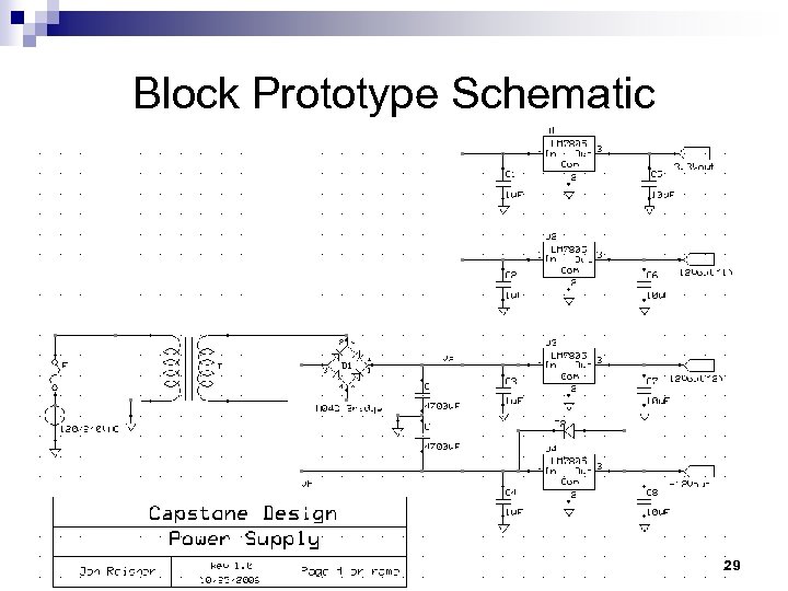
Block Prototype Schematic 29
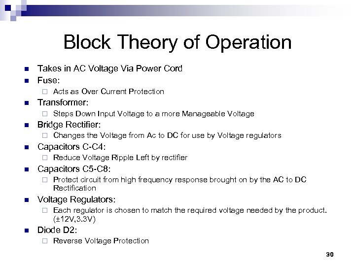
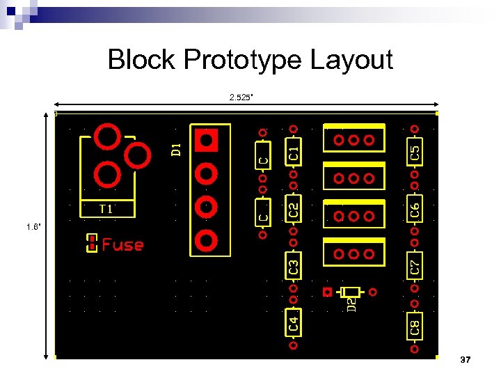
Block Theory of Operation n n Takes in AC Voltage Via Power Cord Fuse: ¨ n Transformer: ¨ n Protect circuit from high frequency response brought on by the AC to DC Rectification Voltage Regulators: ¨ n Reduce Voltage Ripple Left by rectifier Capacitors C 5 -C 8: ¨ n Changes the Voltage from Ac to DC for use by Voltage regulators Capacitors C-C 4: ¨ n Steps Down Input Voltage to a more Manageable Voltage Bridge Rectifier: ¨ n Acts as Over Current Protection Each regulator is chosen to match the required voltage needed by the product. (± 12 V, 3. 3 V) Diode D 2: ¨ Reverse Voltage Protection 30
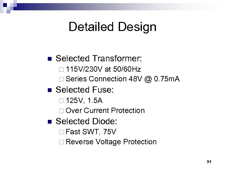
Detailed Design n Selected Transformer: ¨ 115 V/230 V at 50/60 Hz ¨ Series Connection 48 V @ 0. 75 m. A n Selected Fuse: ¨ 125 V, 1. 5 A ¨ Over Current Protection n Selected Diode: ¨ Fast SWT, 75 V ¨ Reverse Voltage Protection 31
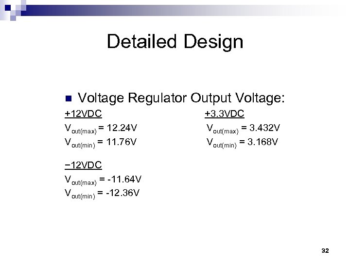
Detailed Design n Voltage Regulator Output Voltage: +12 VDC Vout(max) = 12. 24 V Vout(min) = 11. 76 V +3. 3 VDC Vout(max) = 3. 432 V Vout(min) = 3. 168 V − 12 VDC Vout(max) = -11. 64 V Vout(min) = -12. 36 V 32
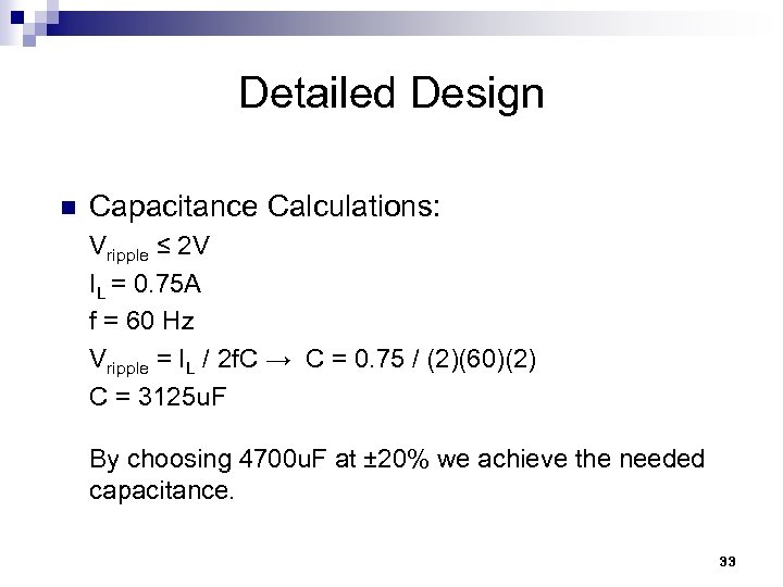
Detailed Design n Capacitance Calculations: Vripple ≤ 2 V IL = 0. 75 A f = 60 Hz Vripple = IL / 2 f. C → C = 0. 75 / (2)(60)(2) C = 3125 u. F By choosing 4700 u. F at ± 20% we achieve the needed capacitance. 33
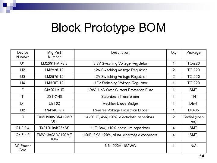
Block Prototype BOM Device Number Mfg Part Number Description Qty Package U 1 LM 2591 HVT-3. 3 3. 3 V Switching Voltage Regulator 1 TO-220 U 2 LM 2576 -12 12 V Switching Voltage Regulator 2 TO-220 U 3 LM 2576 -12 12 V Switching Voltage Regulator 2 TO-220 U 4 LM 320 T-12 -12 V Switching Voltage Regulator 1 TO-220 F 045901. 5 UR 125 V, 1. 5 A Over-Current Protection Fuse 1 SMT T DST-7 -48 Step-down Transformer 1 TH D 1 DB 102 Rectifier Diode Bridge 1 DB-1 D 2 1 N 4148 T/R Reverse Voltage Protection Diode 1 DO-35 C EKMH 500 VSN 472 MR 30 T 4700 u. F, 45 V, ± 20%, electrolytic capacitors 2 Radial (snap -in) C 1, 2, 3, 4 T 491 B 105 K 035 AS 1 u. F, 35 V, ± 10%, tantalum capacitors 4 SMT C 5, 6, 7, 8 EMVH 350 ADA 100 MF 60 G 10 u. F, 35 V, ± 20%, alum. electrolytic capacitors 4 SMT 6’ 6”, 220 V, 18 AWG 1 N/A AC Power Cord 34
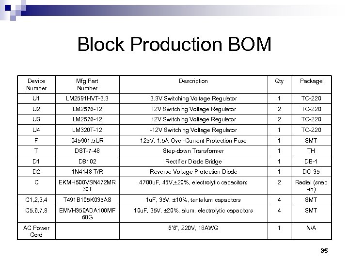
Block Production BOM Device Number Mfg Part Number Description Qty Package U 1 LM 2591 HVT-3. 3 3. 3 V Switching Voltage Regulator 1 TO-220 U 2 LM 2576 -12 12 V Switching Voltage Regulator 2 TO-220 U 3 LM 2576 -12 12 V Switching Voltage Regulator 2 TO-220 U 4 LM 320 T-12 -12 V Switching Voltage Regulator 1 TO-220 F 045901. 5 UR 125 V, 1. 5 A Over-Current Protection Fuse 1 SMT T DST-7 -48 Step-down Transformer 1 TH D 1 DB 102 Rectifier Diode Bridge 1 DB-1 D 2 1 N 4148 T/R Reverse Voltage Protection Diode 1 DO-35 C EKMH 500 VSN 472 MR 30 T 4700 u. F, 45 V, ± 20%, electrolytic capacitors 2 Radial (snap -in) C 1, 2, 3, 4 T 491 B 105 K 035 AS 1 u. F, 35 V, ± 10%, tantalum capacitors 4 SMT C 5, 6, 7, 8 EMVH 350 ADA 100 MF 60 G 10 u. F, 35 V, ± 20%, alum. electrolytic capacitors 4 SMT 6’ 6”, 220 V, 18 AWG 1 N/A AC Power Cord 35
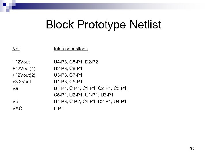
Block Prototype Netlist Net Interconnections − 12 Vout +12 Vout(1) +12 Vout(2) +3. 3 Vout Va U 4 -P 3, C 8 -P 1, D 2 -P 2 U 2 -P 3, C 6 -P 1 U 3 -P 3, C 7 -P 1 U 1 -P 3, C 5 -P 1 D 1 -P 1, C 2 -P 1, C 3 -P 1, C 6 -P 1, U 2 -P 1, U 1 -P 1, U 3 -P 1 D 1 -P 3, C-P 2, C 4 -P 1, D 2 -P 1, U 4 -P 1 F-P 1 Vb VAC 36
Block Prototype Layout 2. 525” 1. 6” 37
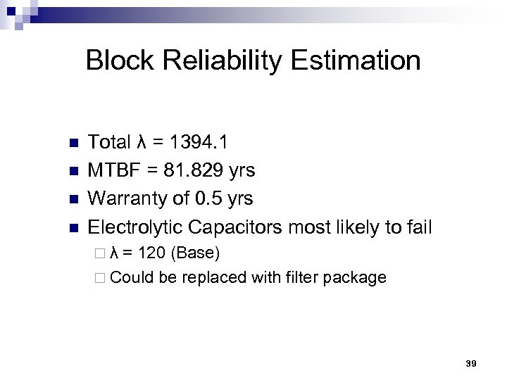
Block Reliability Estimation Component Description Qty Base λ Total λ IC Voltage Regulator (3. 3 V) 1 50 23. 29634 IC Voltage Regulator (12 V) 2 50 59. 26176 IC Voltage Regulator (-12 V) 1 50 29. 63088 Transformer 1 5 283. 1314 Diode Bridge Rectifier 1 4. 8 1. 769135 Electrolytic Capacitor 6 120 477. 4554 Tantalum Capacitor 4 10 26. 5253 Diode 1 1 0. 213577 Fuse 1 70 49. 8740 AC Power Cord 1 105 442. 9243 38
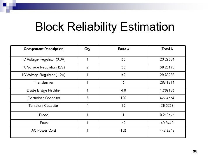
Block Reliability Estimation n n Total λ = 1394. 1 MTBF = 81. 829 yrs Warranty of 0. 5 yrs Electrolytic Capacitors most likely to fail ¨ λ = 120 (Base) ¨ Could be replaced with filter package 39
Block Verification Plan n Using Detailed Design: ¨ Simulate and verify results in Spice ¨ Construct Prototype ¨ Verify results in the lab ¨ Modify if needed 40

MPU w/ RS 232 Port Team 4 Chad Due 41
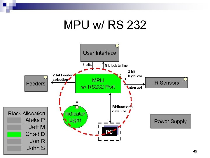
MPU w/ RS 232 User Interface 3 bits Feeders Block Allocation Aleks P. Jeff M. Chad D. Jon R. John S. 2 bit Feeder selection 8 bit data line MPU w/ RS 232 Port Indicator Light 2 bit high/low interrupt IR Sensors Bidirectional data line Power Supply PC 42
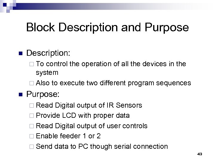
Block Description and Purpose n Description: ¨ To control the operation of all the devices in the system ¨ Also to execute two different program sequences n Purpose: ¨ Read Digital output of IR Sensors ¨ Provide LCD with proper data ¨ Read Digital output of user controls ¨ Enable feeder 1 or 2 ¨ Send data to PC though serial connection 43
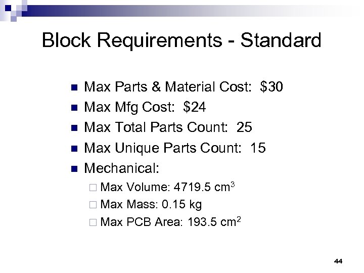
Block Requirements - Standard n n n Max Parts & Material Cost: $30 Max Mfg Cost: $24 Max Total Parts Count: 25 Max Unique Parts Count: 15 Mechanical: ¨ Max Volume: 4719. 5 cm 3 ¨ Max Mass: 0. 15 kg ¨ Max PCB Area: 193. 5 cm 2 44
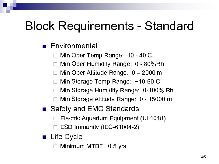
Block Requirements - Standard n Environmental: ¨ ¨ ¨ n Min Oper Temp Range: 10 - 40 C Min Oper Humidity Range: 0 - 80%Rh Min Oper Altitude Range: 0 – 2000 m Min Storage Temp Range: − 10 -60 C Min Storage Humidity Range: 0 -100% Rh Min Storage Altitude Range: 0 - 15000 m Safety and EMC Standards: Electric Aquarium Equipment (UL 1018) ¨ ESD Immunity (IEC-61004 -2) ¨ n Life Cycle ¨ Minimum MTBF: 0. 5 yrs 45
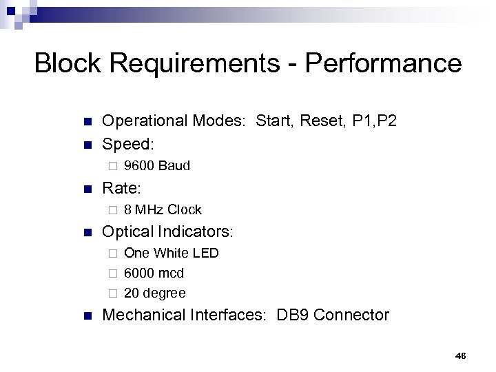
Block Requirements - Performance n n Operational Modes: Start, Reset, P 1, P 2 Speed: ¨ n Rate: ¨ n 9600 Baud 8 MHz Clock Optical Indicators: One White LED ¨ 6000 mcd ¨ 20 degree ¨ n Mechanical Interfaces: DB 9 Connector 46
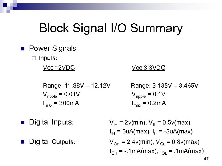
Block Signal I/O Summary n Power Signals ¨ Inputs: Vcc 12 VDC Vcc 3. 3 VDC Range: 11. 88 V – 12. 12 V Range: 3. 135 V – 3. 465 V Vripple = 0. 01 V Vripple = 0. 1 V Imax = 300 m. A Imax = 0. 2 m. A n Digital Inputs: VIH = 2 v(min), VIL = 0. 5 v(max) IIH = 5 u. A(max), IIL = -5 u. A(max) n Digital Outputs: VOH = 2. 4 v(min), VOL = 0. 8 v(max) IOH = -. 1 m. A(max), IOL =. 1 m. A(max) 47
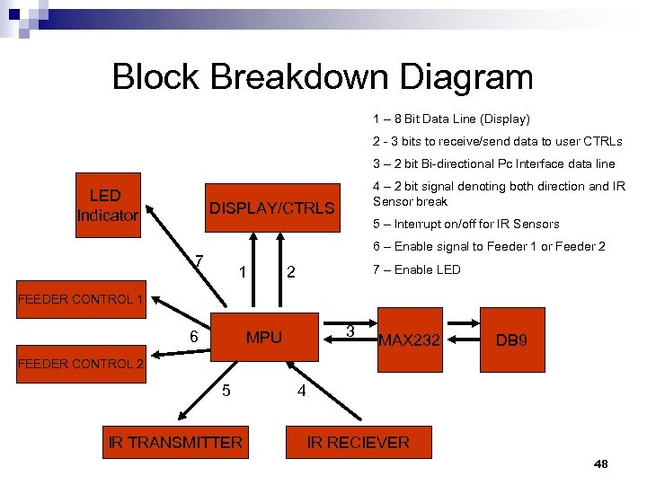
Block Breakdown Diagram 1 – 8 Bit Data Line (Display) 2 - 3 bits to receive/send data to user CTRLs 3 – 2 bit Bi-directional Pc Interface data line LED Indicator 4 – 2 bit signal denoting both direction and IR Sensor break DISPLAY/CTRLS 5 – Interrupt on/off for IR Sensors 6 – Enable signal to Feeder 1 or Feeder 2 7 1 7 – Enable LED 2 FEEDER CONTROL 1 6 3 MPU MAX 232 DB 9 FEEDER CONTROL 2 5 IR TRANSMITTER 4 IR RECIEVER 48
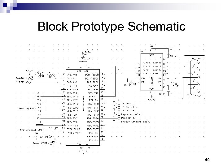
Block Prototype Schematic 49
Block Theory of Operation n 1 – PIC will enable IR Sensors, Get info from User Ctlrs telling program info, display all indicated info, start experiment 2 – When time delay timer gets to zero turn on LED, enable proper feeder, monitor IR senor pins, send data to PC when needed 3 – reset timer and continue experiment, monitor IR sensors, turn off LED, wait for next delay timer zeroing, repeat steps until program sequence ends 50
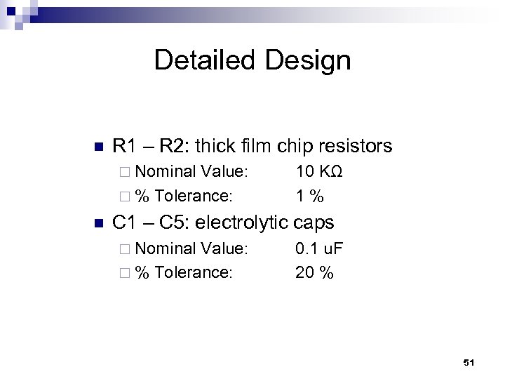
Detailed Design n R 1 – R 2: thick film chip resistors ¨ Nominal Value: ¨ % Tolerance: n 10 KΩ 1 % C 1 – C 5: electrolytic caps ¨ Nominal Value: ¨ % Tolerance: 0. 1 u. F 20 % 51
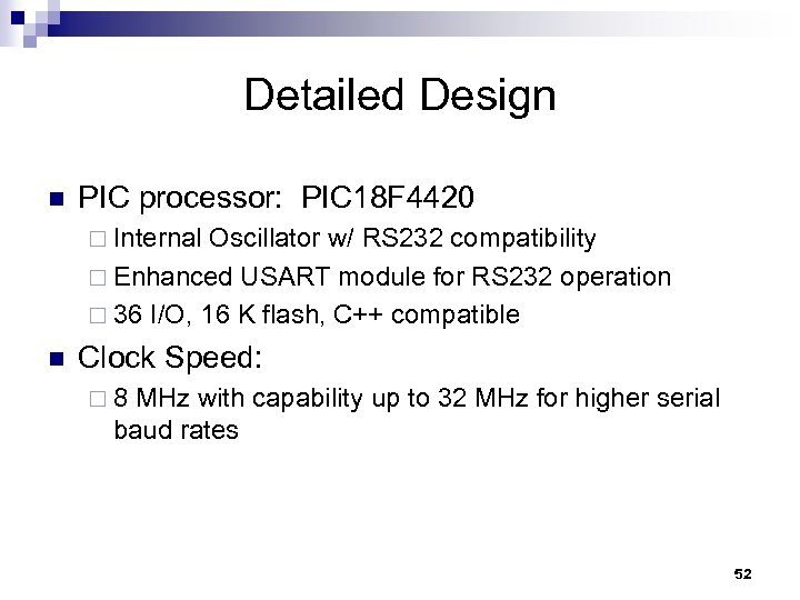
Detailed Design n PIC processor: PIC 18 F 4420 ¨ Internal Oscillator w/ RS 232 compatibility ¨ Enhanced USART module for RS 232 operation ¨ 36 I/O, 16 K flash, C++ compatible n Clock Speed: ¨ 8 MHz with capability up to 32 MHz for higher serial baud rates 52
![Detailed Design n Equations of Baud Rate Error N = [(Fosc/Desired Baud Rate)/64] – Detailed Design n Equations of Baud Rate Error N = [(Fosc/Desired Baud Rate)/64] –](https://present5.com/presentation/b07396b1da8ed6d0f82b9e33fc9778b4/image-53.jpg)
Detailed Design n Equations of Baud Rate Error N = [(Fosc/Desired Baud Rate)/64] – 1 ¨ Calculated Baud Rate = Fosc / [64(N+1)] ¨ Error(%) = (Calculated – Desired) / Desired Baud Rate ¨ n Desired Baud Rate of 9600 @ Fosc of 8 MHz N = 12 ¨ Calculated Baud Rate = 9615. 38 ¨ Error(%) =. 16 % ¨ 53
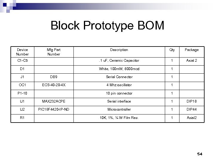
Block Prototype BOM Device Number Mfg Part Number Description Qty Package C 1 -C 5 . 1 u. F, Ceramic Capacitor 1 Axial 2 D 1 White, 100 m. W, 6000 mcd 1 J 1 DB 9 Serial Connector 1 OC 1 ECS-40 -20 -4 X 4 Mhz oscillator 1 10 pin connector 1 P 1 -10 U 1 MAX 232 ACPE Serial interface 1 DIP 16 U 2 PIC 18 F 4420 -IP-ND Microcontroller 1 DIP 44 10 K, 1%, ¼ W Film Res. 1 Axial 2 R 1 54
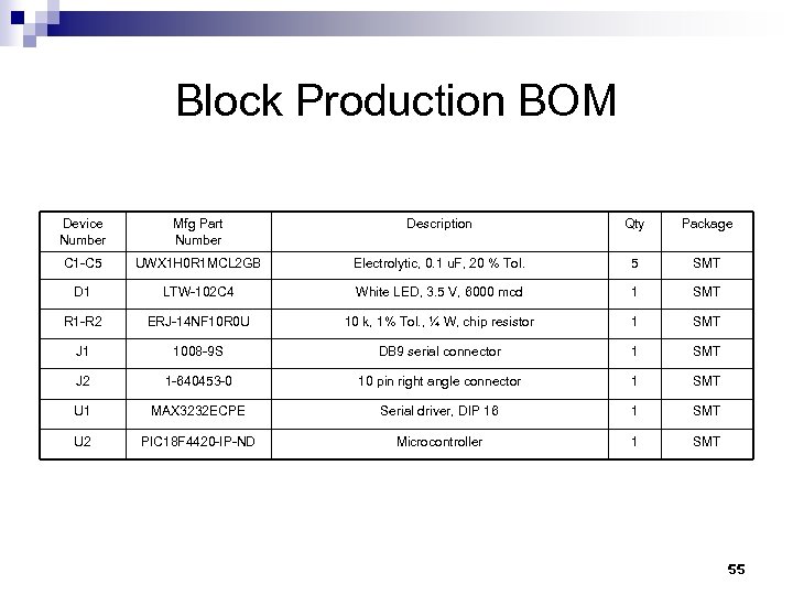
Block Production BOM Device Number Mfg Part Number Description Qty Package C 1 -C 5 UWX 1 H 0 R 1 MCL 2 GB Electrolytic, 0. 1 u. F, 20 % Tol. 5 SMT D 1 LTW-102 C 4 White LED, 3. 5 V, 6000 mcd 1 SMT R 1 -R 2 ERJ-14 NF 10 R 0 U 10 k, 1% Tol. , ¼ W, chip resistor 1 SMT J 1 1008 -9 S DB 9 serial connector 1 SMT J 2 1 -640453 -0 10 pin right angle connector 1 SMT U 1 MAX 3232 ECPE Serial driver, DIP 16 1 SMT U 2 PIC 18 F 4420 -IP-ND Microcontroller 1 SMT 55
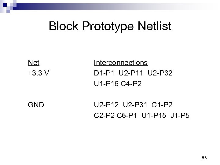
Block Prototype Netlist Net +3. 3 V Interconnections D 1 -P 1 U 2 -P 11 U 2 -P 32 U 1 -P 16 C 4 -P 2 GND U 2 -P 12 U 2 -P 31 C 1 -P 2 C 2 -P 2 C 6 -P 1 U 1 -P 15 J 1 -P 5 56
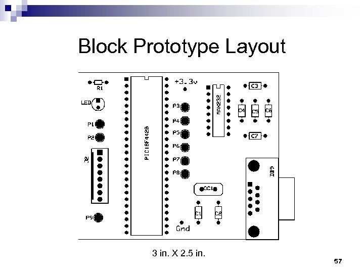
Block Prototype Layout 3 in. X 2. 5 in. 57
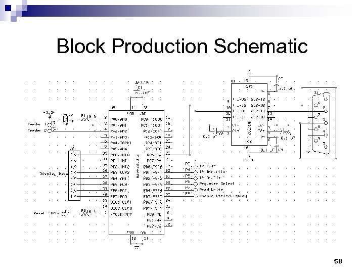
Block Production Schematic 58
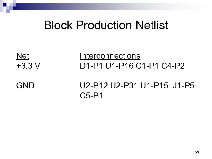
Block Production Netlist Net +3. 3 V Interconnections D 1 -P 1 U 1 -P 16 C 1 -P 1 C 4 -P 2 GND U 2 -P 12 U 2 -P 31 U 1 -P 15 J 1 -P 5 C 5 -P 1 59
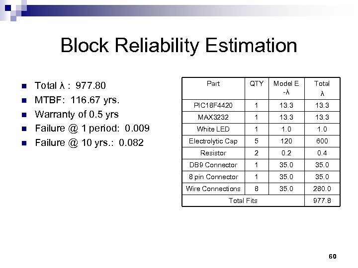
Block Reliability Estimation n n Total λ : 977. 80 MTBF: 116. 67 yrs. Warranty of 0. 5 yrs Failure @ 1 period: 0. 009 Failure @ 10 yrs. : 0. 082 Part QTY Model E -λ Total λ PIC 18 F 4420 1 13. 3 MAX 3232 1 13. 3 White LED 1 1. 0 Electrolytic Cap 5 120 600 Resistor 2 0. 4 DB 9 Connector 1 35. 0 8 pin Connector 1 35. 0 Wire Connections 8 35. 0 280. 0 Total Fits 977. 8 60
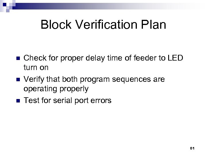
Block Verification Plan n Check for proper delay time of feeder to LED turn on Verify that both program sequences are operating properly Test for serial port errors 61

IR Sensors Team 4 Aleks Plavsic 62
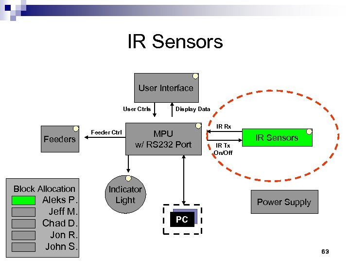
IR Sensors User Interface User Ctrls Feeders Block Allocation Aleks P. Jeff M. Chad D. Jon R. John S. Feeder Ctrl Display Data MPU w/ RS 232 Port Indicator Light IR Rx IR Tx On/Off IR Sensors Power Supply PC 63
Block Description and Purpose n Description: ¨ n Generates 2 vertical and parallel “curtains” of Infrared beams that cover the width and height of fish tank Purpose: Need to detect when a fish specimen crosses from one side of a fish tank to the other – when beam is broken ¨ Need to sense the direction of specimen’s motion ¨ 64
Block Requirements - Standard n n n Max Parts & Material Cost: $150 (25%) Max Mfg Cost: $72 (30%) Max Total Parts Count: 150 (30%) Max Unique Parts Count: 20 (20%) Mechanical Reqs: ¨ ¨ ¨ Max Volume: 23598 cm 2 (25%) Max Mass: 0. 75 kg (25%) Max PCB Area: 96. 75 cm 2 (15%) Max # of PCBs: 2 Max Shock Force: 0. 1 G Max Shock Repetitions: 1 65
Block Requirements - Standard n Environmental Reqs: ¨ ¨ ¨ ¨ n Min Oper Temp Range: 10 - 40°C Min Storage Temp Range: − 10 - 60°C Min Oper Humidity Range: 0 – 80 %Rh Min Storage humidity Range: 0 – 100 %Rh Min Oper Altitude Range: 0 – 2000 m Min Storage/Shipping Altitude Range: 0 – 15000 m Max Storage Duration: 10 yrs Safety and EMC Standards: UL 1018: Electric Aquarium Equipment ¨ IEC-60825 -1: Guidance on Laser Products ¨ IEC-61000 -4 -3: E Field Immunity ¨ IEC-61000 -4 -6: RF Conducted Immunity ¨ n Life Cycle: ¨ Est. Max Production Lifetime: 8 yrs 66
Block Requirements - Performance n n IR Wavelength Range: 700 – 1000 nm IR Signals Output Min. Power = 10 m. W/sr IR Signals Input Min. Power = 5 μW Sensitivity: Min. Detectable Specimen Height: 2 cm ¨ Min. Detectable Specimen Length: 2 cm ¨ n Effectiveness: Min. Time for Correct Detection: 1 ms ¨ Beams’ Coverage Width: 6 in = 15. 24 cm ¨ Beams’ Coverage Height: 6 in = 15. 24 cm ¨ 67
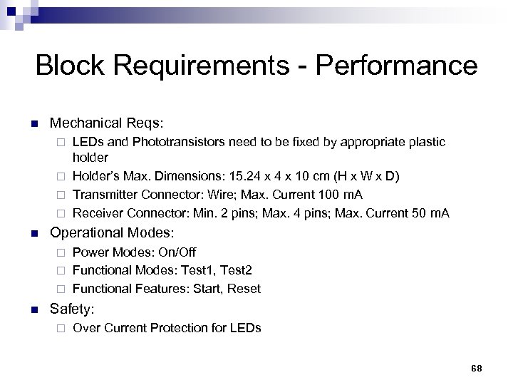
Block Requirements - Performance n Mechanical Reqs: LEDs and Phototransistors need to be fixed by appropriate plastic holder ¨ Holder’s Max. Dimensions: 15. 24 x 10 cm (H x W x D) ¨ Transmitter Connector: Wire; Max. Current 100 m. A ¨ Receiver Connector: Min. 2 pins; Max. 4 pins; Max. Current 50 m. A ¨ n Operational Modes: Power Modes: On/Off ¨ Functional Modes: Test 1, Test 2 ¨ Functional Features: Start, Reset ¨ n Safety: ¨ Over Current Protection for LEDs 68
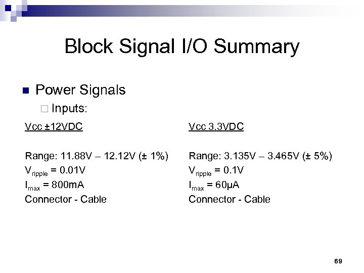
Block Signal I/O Summary n Power Signals ¨ Inputs: Vcc ± 12 VDC Vcc 3. 3 VDC Range: 11. 88 V – 12. 12 V (± 1%) Vripple = 0. 01 V Imax = 800 m. A Connector - Cable Range: 3. 135 V – 3. 465 V (± 5%) Vripple = 0. 1 V Imax = 60µA Connector - Cable 69
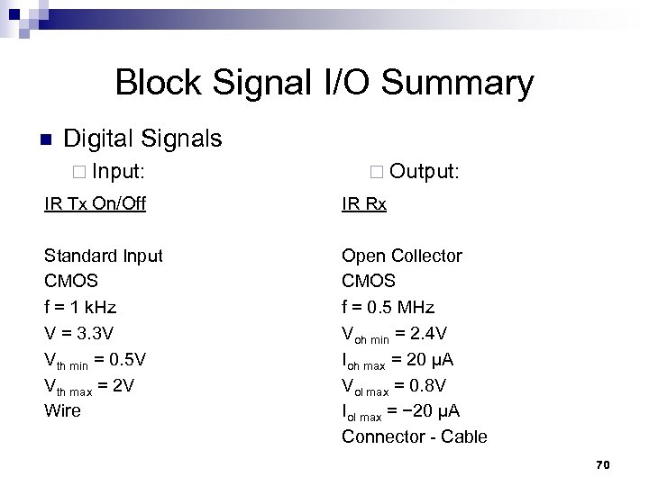
Block Signal I/O Summary n Digital Signals ¨ Input: ¨ Output: IR Tx On/Off IR Rx Standard Input CMOS f = 1 k. Hz V = 3. 3 V Vth min = 0. 5 V Vth max = 2 V Wire Open Collector CMOS f = 0. 5 MHz Voh min = 2. 4 V Ioh max = 20 µA Vol max = 0. 8 V Iol max = − 20 µA Connector - Cable 70
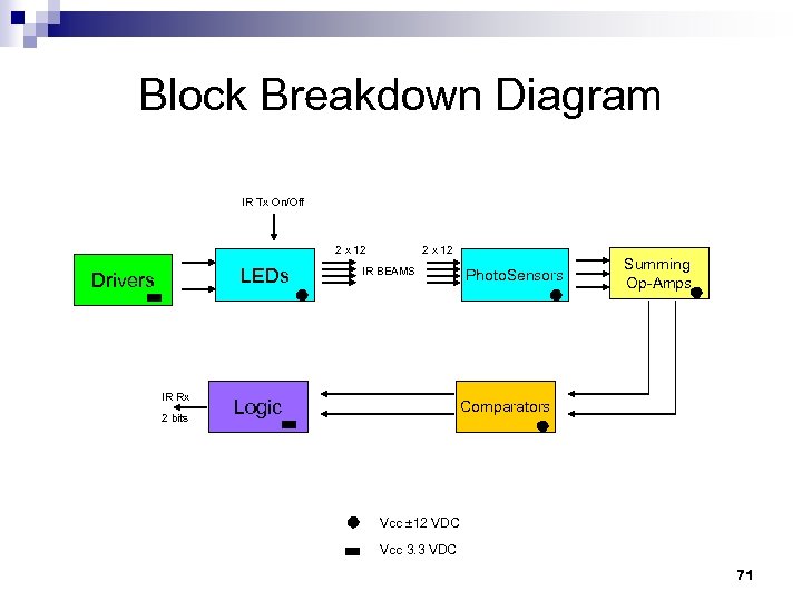
Block Breakdown Diagram IR Tx On/Off 2 x 12 LEDs Drivers IR Rx 2 bits 2 x 12 IR BEAMS Logic Photo. Sensors Summing Op-Amps Comparators Vcc ± 12 VDC Vcc 3. 3 VDC 71
Block Prototype Schematic TX RX 72
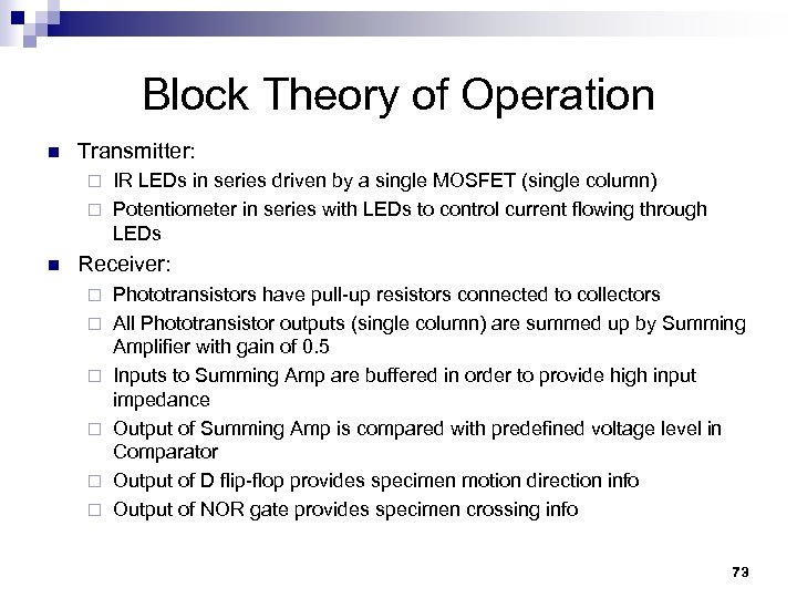
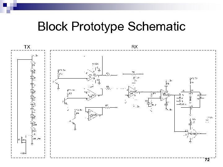
Block Theory of Operation n Transmitter: IR LEDs in series driven by a single MOSFET (single column) ¨ Potentiometer in series with LEDs to control current flowing through LEDs ¨ n Receiver: ¨ ¨ ¨ Phototransistors have pull-up resistors connected to collectors All Phototransistor outputs (single column) are summed up by Summing Amplifier with gain of 0. 5 Inputs to Summing Amp are buffered in order to provide high input impedance Output of Summing Amp is compared with predefined voltage level in Comparator Output of D flip-flop provides specimen motion direction info Output of NOR gate provides specimen crossing info 73
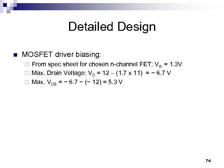
Detailed Design n MOSFET driver biasing: From spec sheet for chosen n-channel FET: Vth = 1. 3 V ¨ Max. Drain Voltage: VD = 12 – (1. 7 x 11) = − 6. 7 V ¨ Max. VDS = − 6. 7 − (− 12) = 5. 3 V ¨ 74
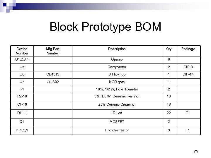
Block Prototype BOM Device Number Mfg Part Number Description Qty U 1, 2, 3, 4 Opamp 8 U 5 Comparator 2 DIP-8 DIP-14 U 6 CD 4013 D Flip-Flop 1 U 7 74 LS 02 NOR gate 1 R 1 10%, 1/2 W, Potentiometer 2 R 2 -10 5%, 1/8 W, Ceramic Resistor 18 C 1 -10 20% Ceramic Capacitor 18 D 1 -11 IR Led 22 Q 1 MOSFET 2 PT 1, 2, 3 Phototransistor 3 Package T 1 75
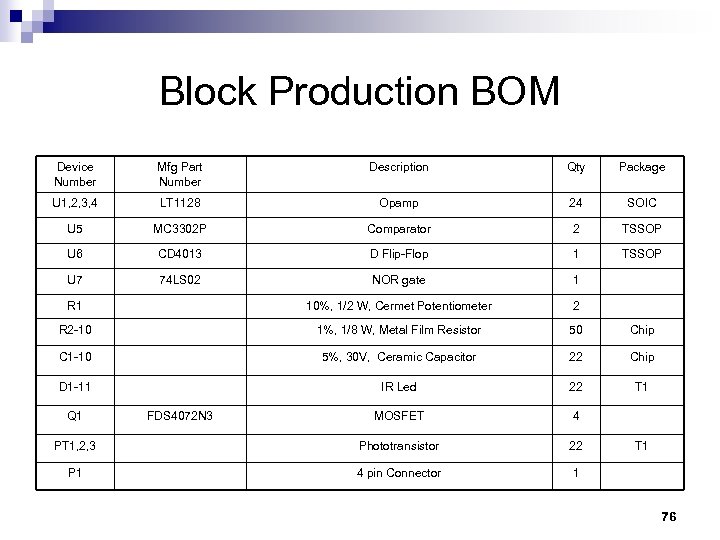
Block Production BOM Device Number Mfg Part Number Description Qty Package U 1, 2, 3, 4 LT 1128 Opamp 24 SOIC U 5 MC 3302 P Comparator 2 TSSOP U 6 CD 4013 D Flip-Flop 1 TSSOP U 7 74 LS 02 NOR gate 1 R 1 10%, 1/2 W, Cermet Potentiometer 2 R 2 -10 1%, 1/8 W, Metal Film Resistor 50 Chip C 1 -10 5%, 30 V, Ceramic Capacitor 22 Chip D 1 -11 IR Led 22 T 1 MOSFET 4 PT 1, 2, 3 Phototransistor 22 P 1 4 pin Connector 1 Q 1 FDS 4072 N 3 T 1 76
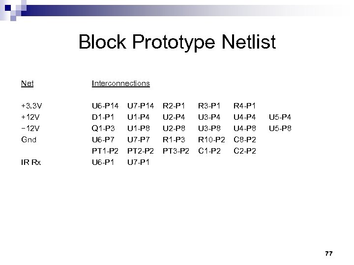
Block Prototype Netlist Net Interconnections +3. 3 V +12 V − 12 V Gnd U 6 -P 14 D 1 -P 1 Q 1 -P 3 U 6 -P 7 PT 1 -P 2 U 6 -P 1 IR Rx U 7 -P 14 U 1 -P 8 U 7 -P 7 PT 2 -P 2 U 7 -P 1 R 2 -P 1 U 2 -P 4 U 2 -P 8 R 1 -P 3 PT 3 -P 2 R 3 -P 1 U 3 -P 4 U 3 -P 8 R 10 -P 2 C 1 -P 2 R 4 -P 1 U 4 -P 4 U 4 -P 8 C 8 -P 2 C 2 -P 2 U 5 -P 4 U 5 -P 8 77
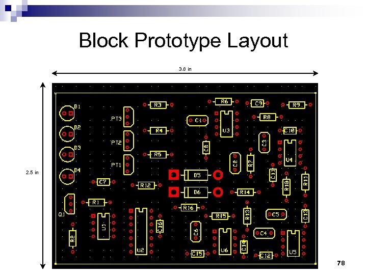
Block Prototype Layout 3. 8 in 2. 5 in 78
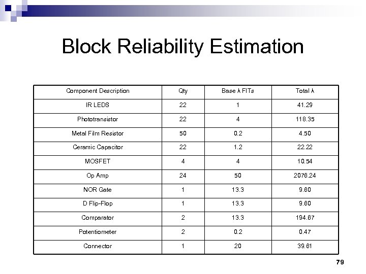
Block Reliability Estimation Component Description Qty Base λ FITs Total λ IR LEDS 22 1 41. 29 Phototransistor 22 4 118. 35 Metal Film Resistor 50 0. 2 4. 50 Ceramic Capacitor 22 1. 2 22. 22 MOSFET 4 4 10. 54 Op Amp 24 50 2076. 24 NOR Gate 1 13. 3 9. 60 D Flip-Flop 1 13. 3 9. 60 Comparator 2 13. 3 194. 67 Potentiometer 2 0. 47 Connector 1 20 39. 61 79
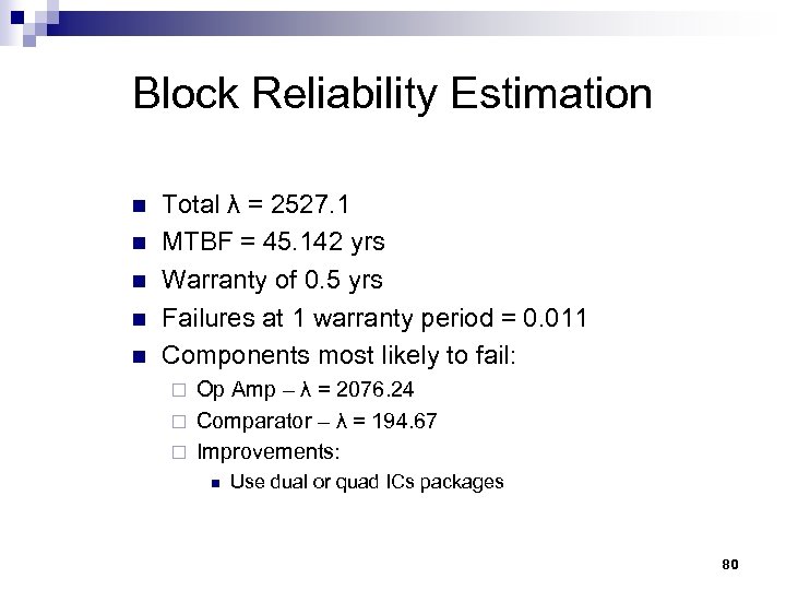
Block Reliability Estimation n n Total λ = 2527. 1 MTBF = 45. 142 yrs Warranty of 0. 5 yrs Failures at 1 warranty period = 0. 011 Components most likely to fail: Op Amp – λ = 2076. 24 ¨ Comparator – λ = 194. 67 ¨ Improvements: ¨ n Use dual or quad ICs packages 80
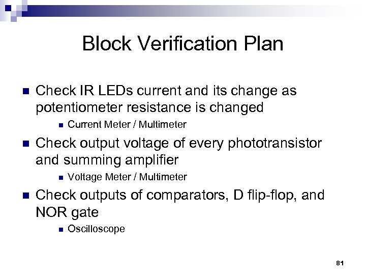
Block Verification Plan n Check IR LEDs current and its change as potentiometer resistance is changed n n Check output voltage of every phototransistor and summing amplifier n n Current Meter / Multimeter Voltage Meter / Multimeter Check outputs of comparators, D flip-flop, and NOR gate n Oscilloscope 81

User Interface & Display Team 4 Jeff Mueller 82
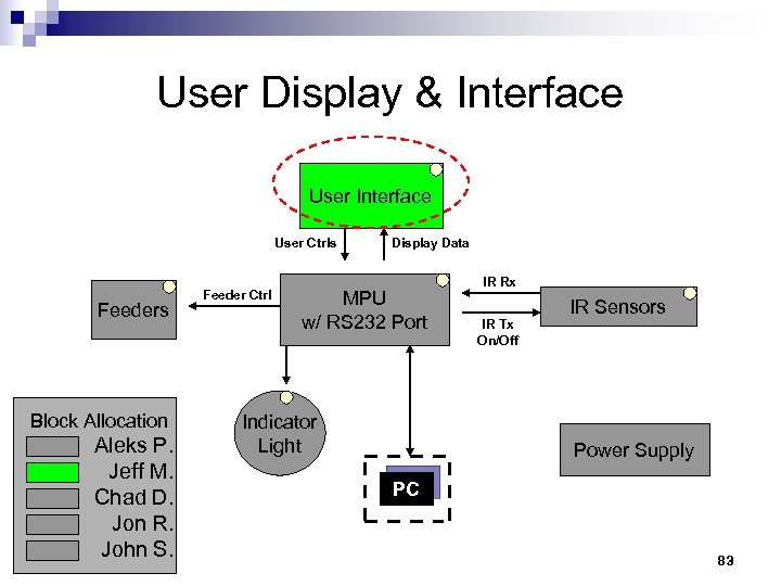
User Display & Interface User Ctrls Feeders Block Allocation Aleks P. Jeff M. Chad D. Jon R. John S. Feeder Ctrl Display Data MPU w/ RS 232 Port Indicator Light IR Rx IR Tx On/Off IR Sensors Power Supply PC 83
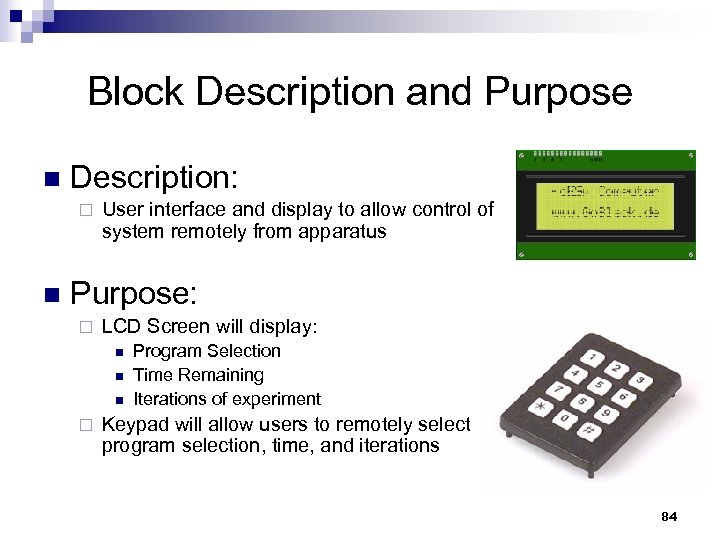
Block Description and Purpose n Description: ¨ n User interface and display to allow control of system remotely from apparatus Purpose: ¨ LCD Screen will display: n n n ¨ Program Selection Time Remaining Iterations of experiment Keypad will allow users to remotely select program selection, time, and iterations 84
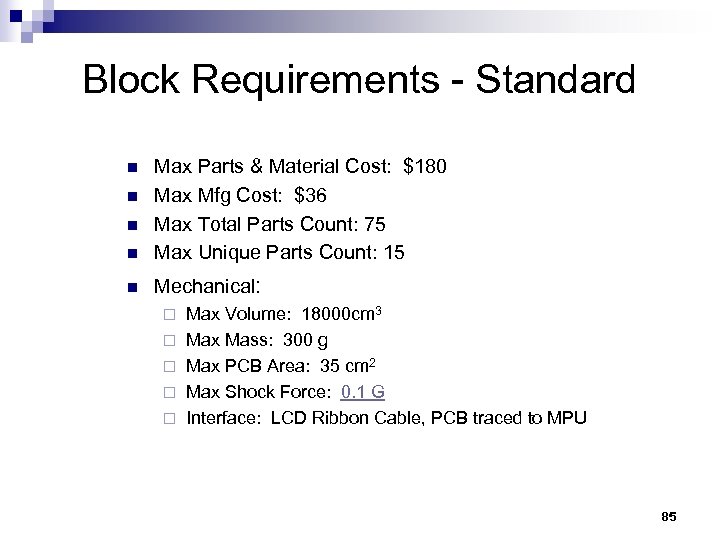
Block Requirements - Standard n Max Parts & Material Cost: $180 Max Mfg Cost: $36 Max Total Parts Count: 75 Max Unique Parts Count: 15 n Mechanical: n n n ¨ ¨ ¨ Max Volume: 18000 cm 3 Max Mass: 300 g Max PCB Area: 35 cm 2 Max Shock Force: 0. 1 G Interface: LCD Ribbon Cable, PCB traced to MPU 85
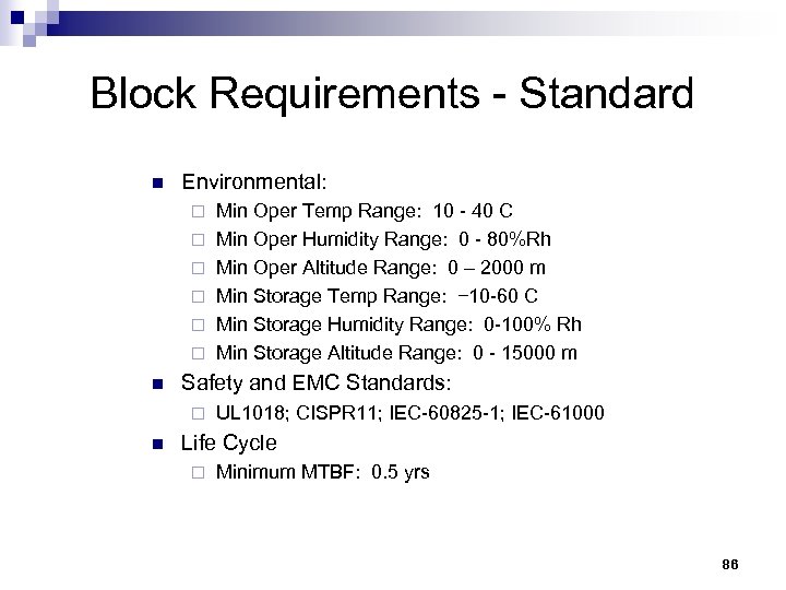
Block Requirements - Standard n Environmental: ¨ ¨ ¨ n Safety and EMC Standards: ¨ n Min Oper Temp Range: 10 - 40 C Min Oper Humidity Range: 0 - 80%Rh Min Oper Altitude Range: 0 – 2000 m Min Storage Temp Range: − 10 -60 C Min Storage Humidity Range: 0 -100% Rh Min Storage Altitude Range: 0 - 15000 m UL 1018; CISPR 11; IEC-60825 -1; IEC-61000 Life Cycle ¨ Minimum MTBF: 0. 5 yrs 86
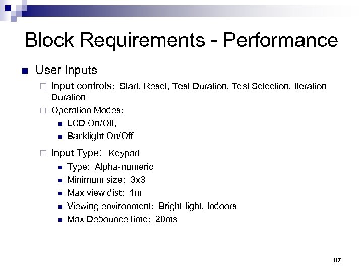
Block Requirements - Performance n User Inputs ¨ Input controls: Start, Reset, Test Duration, Test Selection, Iteration Duration ¨ Operation Modes: n LCD On/Off, n Backlight On/Off ¨ Input Type: Keypad n n n Type: Alpha-numeric Minimum size: 3 x 3 Max view dist: 1 m Viewing environment: Bright light, Indoors Max Debounce time: 20 ms 87
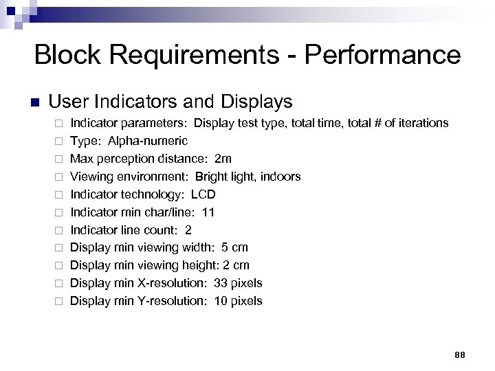
Block Requirements - Performance n User Indicators and Displays ¨ ¨ ¨ Indicator parameters: Display test type, total time, total # of iterations Type: Alpha-numeric Max perception distance: 2 m Viewing environment: Bright light, indoors Indicator technology: LCD Indicator min char/line: 11 Indicator line count: 2 Display min viewing width: 5 cm Display min viewing height: 2 cm Display min X-resolution: 33 pixels Display min Y-resolution: 10 pixels 88
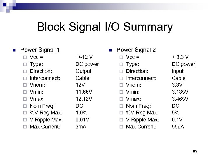
Block Signal I/O Summary n Power Signal 1 ¨ ¨ ¨ Vcc = Type: Direction: Interconnect: Vnom: Vmin: Vmax: Nom Freq: %V-Reg Max: V-Ripple Max: Max Current: n +/-12 V DC power Output Cable 12 V 11. 88 V 12. 12 V DC 1. 0% 0. 01 V 3 m. A Power Signal 2 ¨ ¨ ¨ Vcc = Type: Direction: Interconnect: Vnom: Vmin: Vmax: Nom Freq: %V-Reg Max: V-Ripple Max: Max Current: + 3. 3 V DC power Input Cable 3. 3 V 3. 135 V 3. 465 V DC 5% 0. 1 V 55 u. A 89
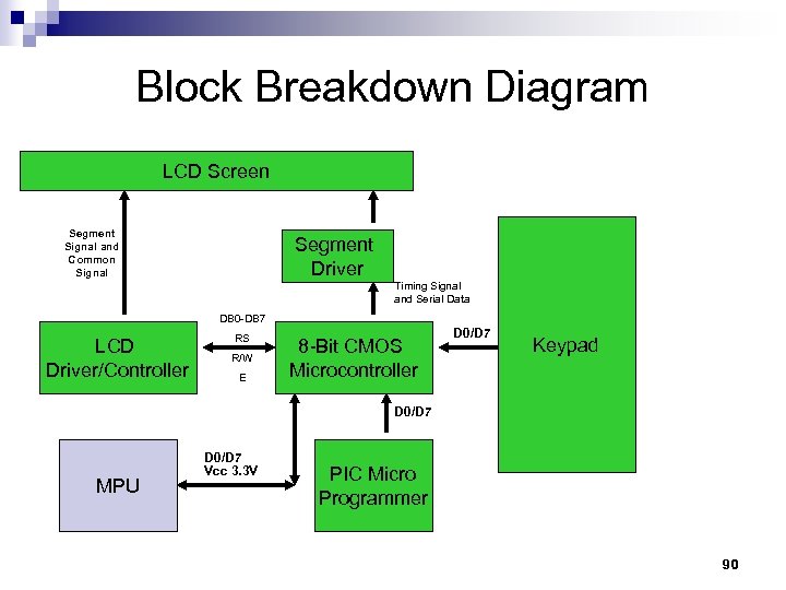
Block Breakdown Diagram LCD Screen Segment Signal and Common Signal Segment Driver Timing Signal and Serial Data DB 0 -DB 7 LCD Driver/Controller RS R/W E 8 -Bit CMOS Microcontroller D 0/D 7 Keypad D 0/D 7 MPU D 0/D 7 Vcc 3. 3 V PIC Micro Programmer 90
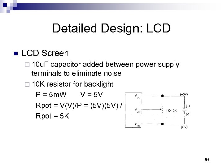
Detailed Design: LCD n LCD Screen ¨ 10 u. F capacitor added between power supply terminals to eliminate noise ¨ 10 K resistor for backlight P = 5 m. W V = 5 V Rpot = V(V)/P = (5 V) / 5 m. W Rpot = 5 K 91
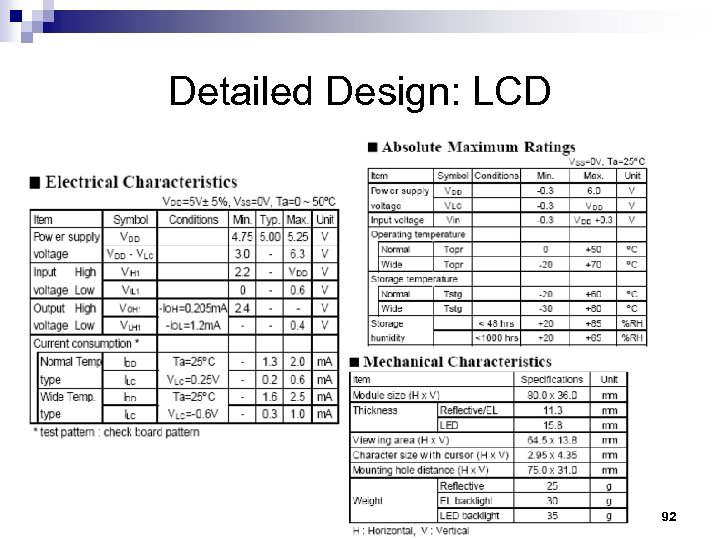
Detailed Design: LCD 92
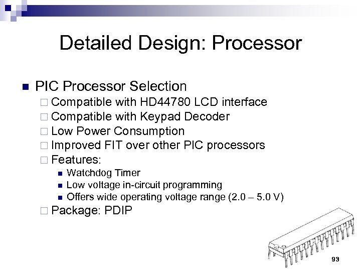
Detailed Design: Processor n PIC Processor Selection ¨ Compatible with HD 44780 LCD interface ¨ Compatible with Keypad Decoder ¨ Low Power Consumption ¨ Improved FIT over other PIC processors ¨ Features: n Watchdog Timer n Low voltage in-circuit programming n Offers wide operating voltage range (2. 0 – 5. 0 V) ¨ Package: PDIP 93
Detailed Design: Processor 94
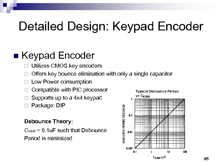
Detailed Design: Keypad Encoder n Keypad Encoder ¨ ¨ ¨ Utilizes CMOS key encoders Offers key bounce elimination with only a single capacitor Low Power consumption Compatible with PIC processor Supports up to a 4 x 4 keypad Package: DIP Debounce Theory: CKBM = 0. 1 u. F such that Debounce Period is minimized 95
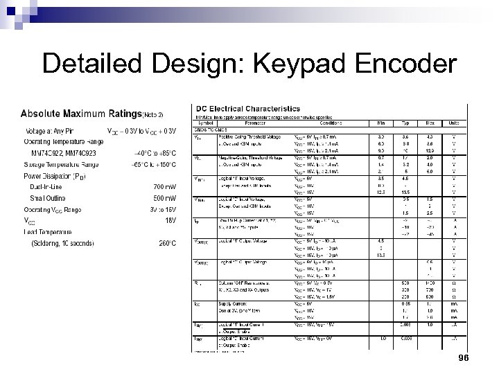
Detailed Design: Keypad Encoder 96
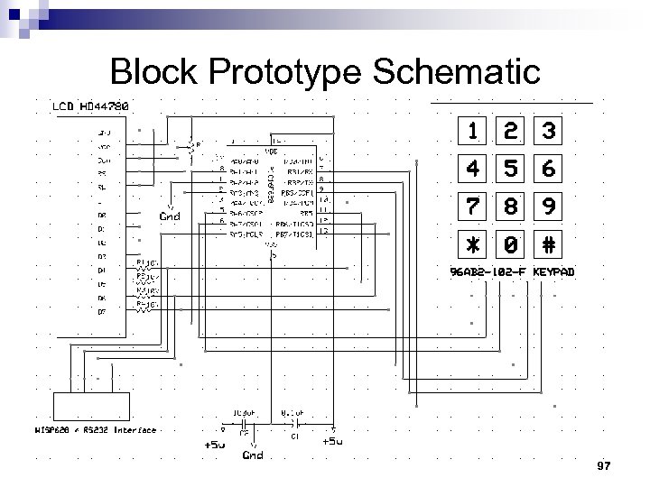
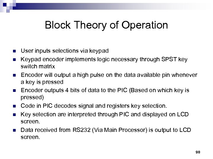
Block Prototype Schematic 97
Block Theory of Operation n n n User inputs selections via keypad Keypad encoder implements logic necessary through SPST key switch matrix Encoder will output a high pulse on the data available pin whenever a key is pressed Encoder outputs 4 bits of data to the PIC (Based on which key is pressed) Code in PIC decodes signal and registers key selection. Key selection are interpreted through PIC and displayed on LCD screen. Data received from RS 232 (Via Main Processor) is output to LCD screen. 98
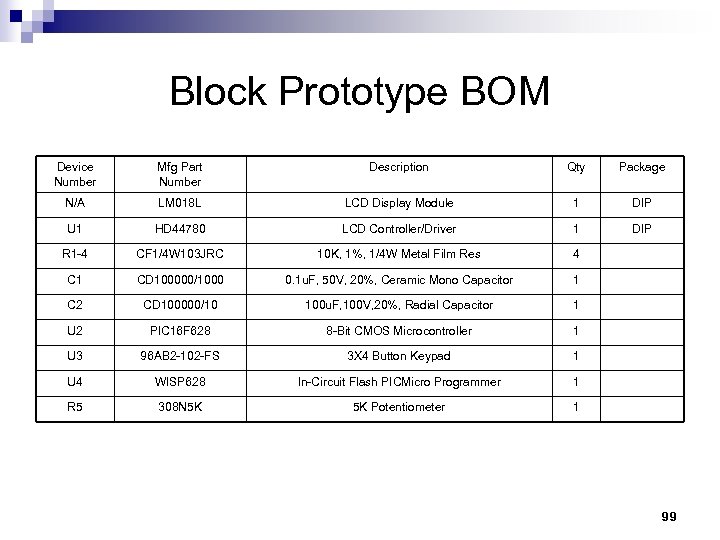
Block Prototype BOM Device Number Mfg Part Number Description Qty Package N/A LM 018 L LCD Display Module 1 DIP U 1 HD 44780 LCD Controller/Driver 1 DIP R 1 -4 CF 1/4 W 103 JRC 10 K, 1%, 1/4 W Metal Film Res 4 C 1 CD 100000/1000 0. 1 u. F, 50 V, 20%, Ceramic Mono Capacitor 1 C 2 CD 100000/10 100 u. F, 100 V, 20%, Radial Capacitor 1 U 2 PIC 16 F 628 8 -Bit CMOS Microcontroller 1 U 3 96 AB 2 -102 -FS 3 X 4 Button Keypad 1 U 4 WISP 628 In-Circuit Flash PICMicro Programmer 1 R 5 308 N 5 K 5 K Potentiometer 1 99
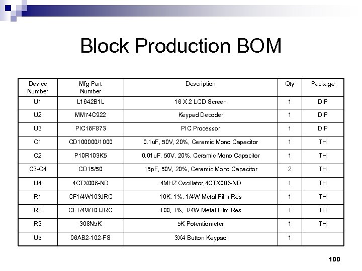
Block Production BOM Device Number Mfg Part Number Description Qty Package U 1 L 1642 B 1 L 16 X 2 LCD Screen 1 DIP U 2 MM 74 C 922 Keypad Decoder 1 DIP U 3 PIC 16 F 873 PIC Processor 1 DIP C 1 CD 100000/1000 0. 1 u. F, 50 V, 20%, Ceramic Mono Capacitor 1 TH C 2 P 10 R 103 K 5 0. 01 u. F, 50 V, 20%, Ceramic Mono Capacitor 1 TH C 3 -C 4 CD 15/50 15 p. F, 50 V, 20%, Ceramic Mono Capacitor 2 TH U 4 4 CTX 006 -ND 4 MHZ Oscillator, 4 CTX 006 -ND 1 TH R 1 CF 1/4 W 103 JRC 10 K, 1%, 1/4 W Metal Film Res 1 TH R 2 CF 1/4 W 101 JRC 100, 1%, 1/4 W Metal Film Res 1 TH R 3 308 N 5 K 5 K Potentiometer 1 TH U 5 96 AB 2 -102 -FS 3 X 4 Button Keypad 1 100
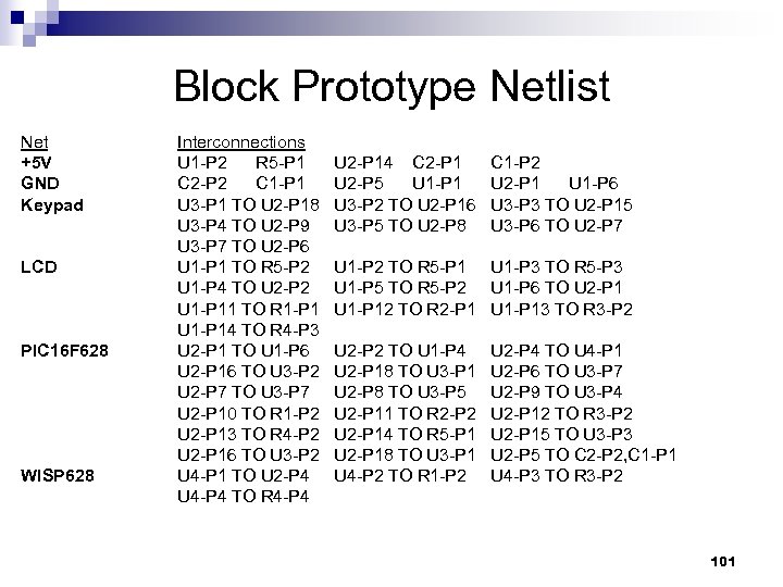
Block Prototype Netlist Net +5 V GND Keypad LCD PIC 16 F 628 WISP 628 Interconnections U 1 -P 2 R 5 -P 1 C 2 -P 2 C 1 -P 1 U 3 -P 1 TO U 2 -P 18 U 3 -P 4 TO U 2 -P 9 U 3 -P 7 TO U 2 -P 6 U 1 -P 1 TO R 5 -P 2 U 1 -P 4 TO U 2 -P 2 U 1 -P 11 TO R 1 -P 1 U 1 -P 14 TO R 4 -P 3 U 2 -P 1 TO U 1 -P 6 U 2 -P 16 TO U 3 -P 2 U 2 -P 7 TO U 3 -P 7 U 2 -P 10 TO R 1 -P 2 U 2 -P 13 TO R 4 -P 2 U 2 -P 16 TO U 3 -P 2 U 4 -P 1 TO U 2 -P 4 U 4 -P 4 TO R 4 -P 4 U 2 -P 14 C 2 -P 1 U 2 -P 5 U 1 -P 1 U 3 -P 2 TO U 2 -P 16 U 3 -P 5 TO U 2 -P 8 C 1 -P 2 U 2 -P 1 U 1 -P 6 U 3 -P 3 TO U 2 -P 15 U 3 -P 6 TO U 2 -P 7 U 1 -P 2 TO R 5 -P 1 U 1 -P 3 TO R 5 -P 3 U 1 -P 5 TO R 5 -P 2 U 1 -P 6 TO U 2 -P 1 U 1 -P 12 TO R 2 -P 1 U 1 -P 13 TO R 3 -P 2 U 2 -P 2 TO U 1 -P 4 U 2 -P 18 TO U 3 -P 1 U 2 -P 8 TO U 3 -P 5 U 2 -P 11 TO R 2 -P 2 U 2 -P 14 TO R 5 -P 1 U 2 -P 18 TO U 3 -P 1 U 4 -P 2 TO R 1 -P 2 U 2 -P 4 TO U 4 -P 1 U 2 -P 6 TO U 3 -P 7 U 2 -P 9 TO U 3 -P 4 U 2 -P 12 TO R 3 -P 2 U 2 -P 15 TO U 3 -P 3 U 2 -P 5 TO C 2 -P 2, C 1 -P 1 U 4 -P 3 TO R 3 -P 2 101
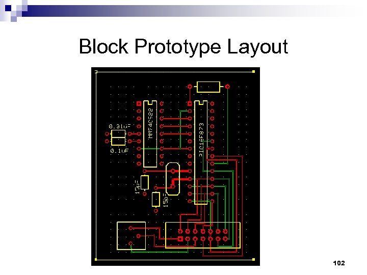
Block Prototype Layout 102
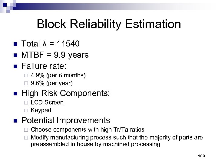
Block Reliability Estimation n Total λ = 11540 MTBF = 9. 9 years Failure rate: 4. 9% (per 6 months) ¨ 9. 6% (per year) ¨ n High Risk Components: LCD Screen ¨ Keypad ¨ n Potential Improvements Choose components with high Tr/Ta ratios ¨ Modify manufacturing process such that the majority of parts are preassembled in house by machined processing ¨ 103
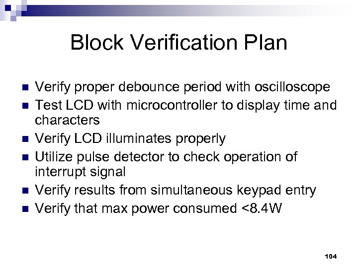
Block Verification Plan n n n Verify proper debounce period with oscilloscope Test LCD with microcontroller to display time and characters Verify LCD illuminates properly Utilize pulse detector to check operation of interrupt signal Verify results from simultaneous keypad entry Verify that max power consumed <8. 4 W 104

Feeder System Team 4 John Schwittay 105
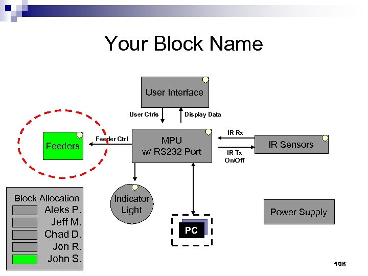
Your Block Name User Interface User Ctrls Feeders Block Allocation Aleks P. Jeff M. Chad D. Jon R. John S. Feeder Ctrl Display Data MPU w/ RS 232 Port Indicator Light IR Rx IR Tx On/Off IR Sensors Power Supply PC 106
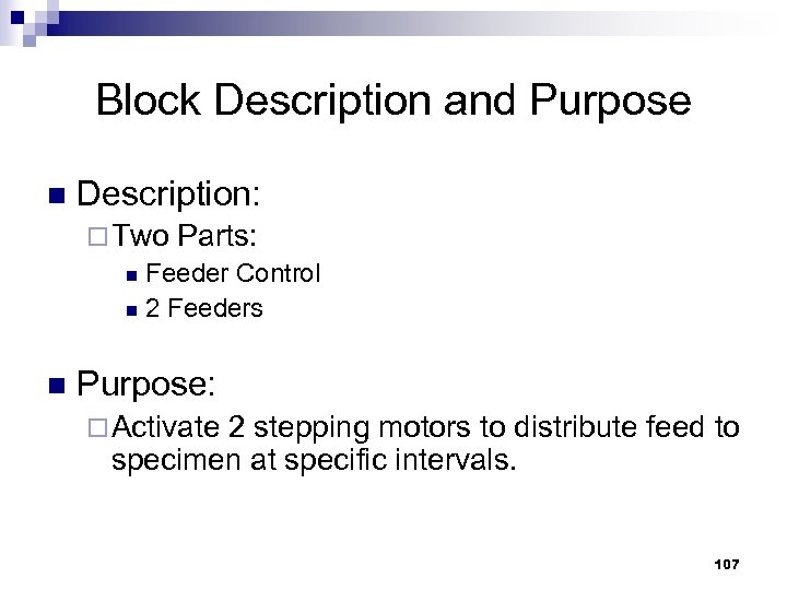
Block Description and Purpose n Description: ¨ Two Parts: n Feeder Control n 2 Feeders n Purpose: ¨ Activate 2 stepping motors to distribute feed to specimen at specific intervals. 107
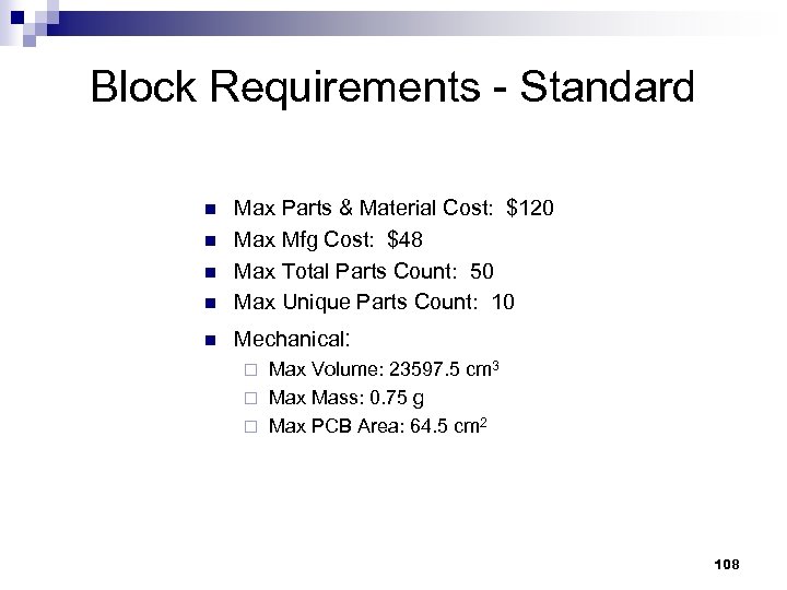
Block Requirements - Standard n Max Parts & Material Cost: $120 Max Mfg Cost: $48 Max Total Parts Count: 50 Max Unique Parts Count: 10 n Mechanical: n n n Max Volume: 23597. 5 cm 3 ¨ Max Mass: 0. 75 g ¨ Max PCB Area: 64. 5 cm 2 ¨ 108
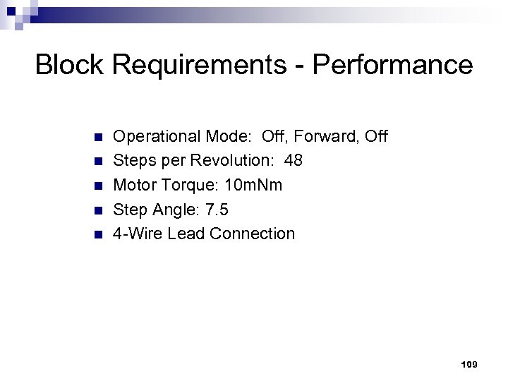
Block Requirements - Performance n n n Operational Mode: Off, Forward, Off Steps per Revolution: 48 Motor Torque: 10 m. Nm Step Angle: 7. 5 4 -Wire Lead Connection 109
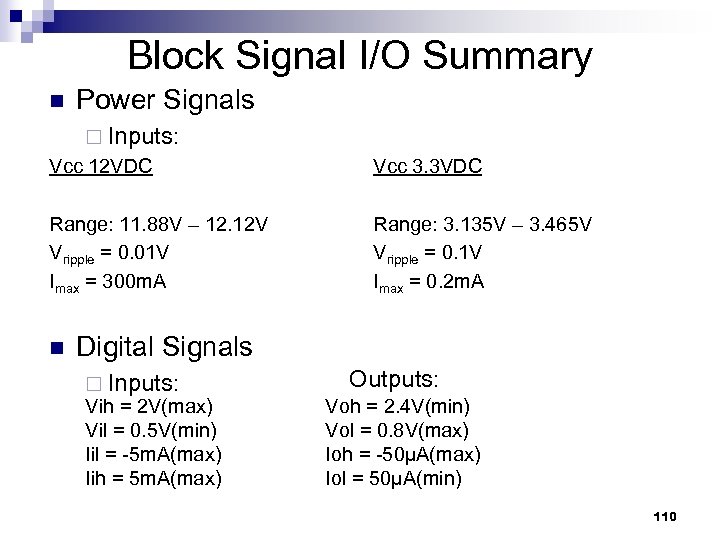
Block Signal I/O Summary n Power Signals ¨ Inputs: Vcc 12 VDC Vcc 3. 3 VDC Range: 11. 88 V – 12. 12 V Vripple = 0. 01 V Imax = 300 m. A Range: 3. 135 V – 3. 465 V Vripple = 0. 1 V Imax = 0. 2 m. A n Digital Signals ¨ Inputs: Vih = 2 V(max) Vil = 0. 5 V(min) Iil = -5 m. A(max) Iih = 5 m. A(max) Outputs: Voh = 2. 4 V(min) Vol = 0. 8 V(max) Ioh = -50µA(max) Iol = 50µA(min) 110
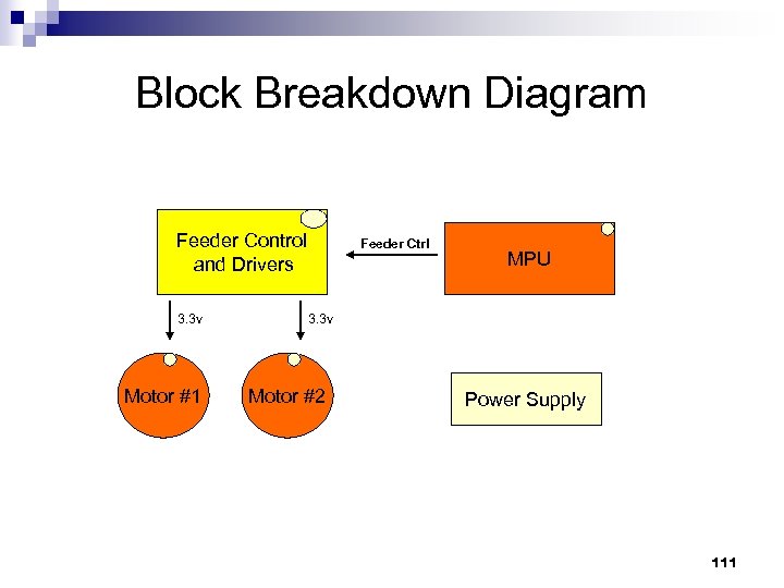
Block Breakdown Diagram Feeder Control and Drivers 3. 3 v Motor #1 Feeder Ctrl MPU 3. 3 v Motor #2 Power Supply 111
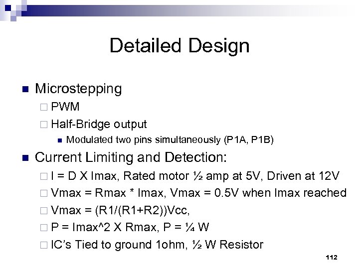
Detailed Design n Microstepping ¨ PWM ¨ Half-Bridge output n n Modulated two pins simultaneously (P 1 A, P 1 B) Current Limiting and Detection: ¨ I = D X Imax, Rated motor ½ amp at 5 V, Driven at 12 V ¨ Vmax = Rmax * Imax, Vmax = 0. 5 V when Imax reached ¨ Vmax = (R 1/(R 1+R 2))Vcc, ¨ P = Imax^2 X Rmax, P = ¼ W ¨ IC’s Tied to ground 1 ohm, ½ W Resistor 112
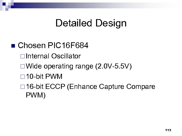
Detailed Design n Chosen PIC 16 F 684 ¨ Internal Oscillator ¨ Wide operating range (2. 0 V-5. 5 V) ¨ 10 -bit PWM ¨ 16 -bit ECCP (Enhance Capture Compare PWM) 113
Detailed Design - 3 n Two logic-input CMOS quad drivers ¨ TC 4467 (NAND) Four on-chip ¨ TC 4468 (AND) Four on-chip ¨ Inputs of the AND gates on the TC 4468 tied together because IC is used as a noninverting MOSFET driver 114
Block Prototype Schematic 115

Block Theory of Operation Utilize signals from MPU n Send signals to the appropriate driver n To activate the proper windings. n 116
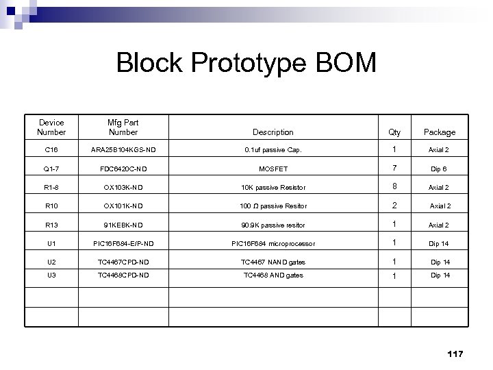
Block Prototype BOM Device Number Mfg Part Number Description Qty Package C 16 ARA 25 B 104 KGS-ND 0. 1 uf passive Cap. 1 Axial 2 Q 1 -7 FDC 6420 C-ND MOSFET 7 Dip 6 R 1 -8 OX 103 K-ND 10 K passive Resistor 8 Axial 2 R 10 OX 101 K-ND 100 Ω passive Resitor 2 Axial 2 R 13 91 KEBK-ND 90. 9 K passive resitor 1 Axial 2 U 1 PIC 16 F 684 -E/P-ND PIC 16 F 684 microprocessor 1 Dip 14 U 2 TC 4467 CPD-ND TC 4467 NAND gates 1 Dip 14 U 3 TC 4468 CPD-ND TC 4468 AND gates 1 Dip 14 117
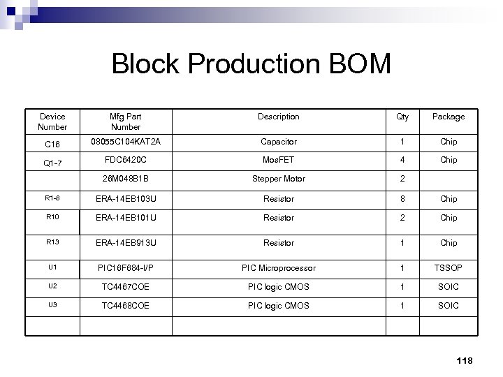
Block Production BOM Device Number Mfg Part Number Description Qty Package C 16 08055 C 104 KAT 2 A Capacitor 1 Chip Q 1 -7 FDC 6420 C Mos. FET 4 Chip 26 M 048 B 1 B Stepper Motor 2 R 1 -8 ERA-14 EB 103 U Resistor 8 Chip R 10 ERA-14 EB 101 U Resistor 2 Chip R 13 ERA-14 EB 913 U Resistor 1 Chip U 1 PIC 16 F 684 -I/P PIC Microprocessor 1 TSSOP U 2 TC 4467 COE PIC logic CMOS 1 SOIC U 3 TC 4468 COE PIC logic CMOS 1 SOIC 118
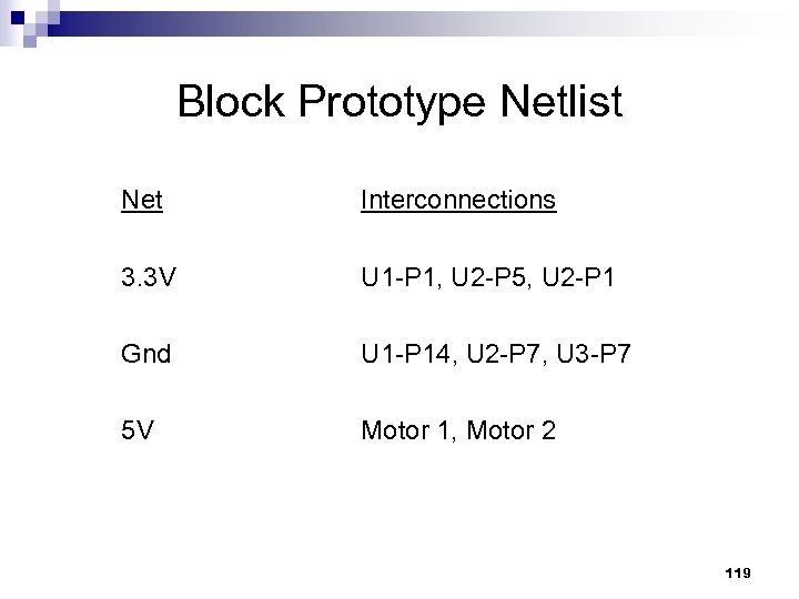
Block Prototype Netlist Net Interconnections 3. 3 V U 1 -P 1, U 2 -P 5, U 2 -P 1 Gnd U 1 -P 14, U 2 -P 7, U 3 -P 7 5 V Motor 1, Motor 2 119
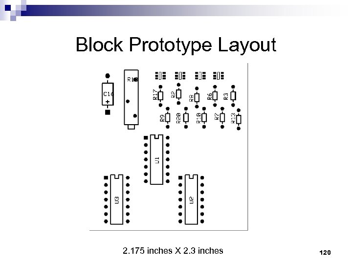
Block Prototype Layout 2. 175 inches X 2. 3 inches 120
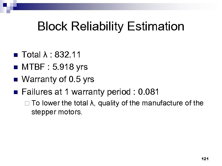
Block Reliability Estimation n n Total λ : 832. 11 MTBF : 5. 918 yrs Warranty of 0. 5 yrs Failures at 1 warranty period : 0. 081 ¨ To lower the total λ, quality of the manufacture of the stepper motors. 121
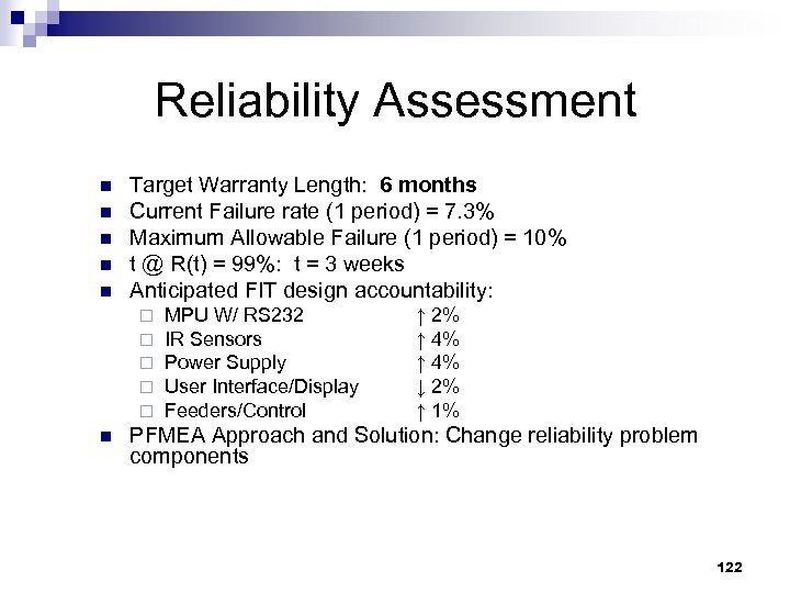
Reliability Assessment n n n Target Warranty Length: 6 months Current Failure rate (1 period) = 7. 3% Maximum Allowable Failure (1 period) = 10% t @ R(t) = 99%: t = 3 weeks Anticipated FIT design accountability: ¨ ¨ ¨ n MPU W/ RS 232 IR Sensors Power Supply User Interface/Display Feeders/Control ↑ 2% ↑ 4% ↓ 2% ↑ 1% PFMEA Approach and Solution: Change reliability problem components 122
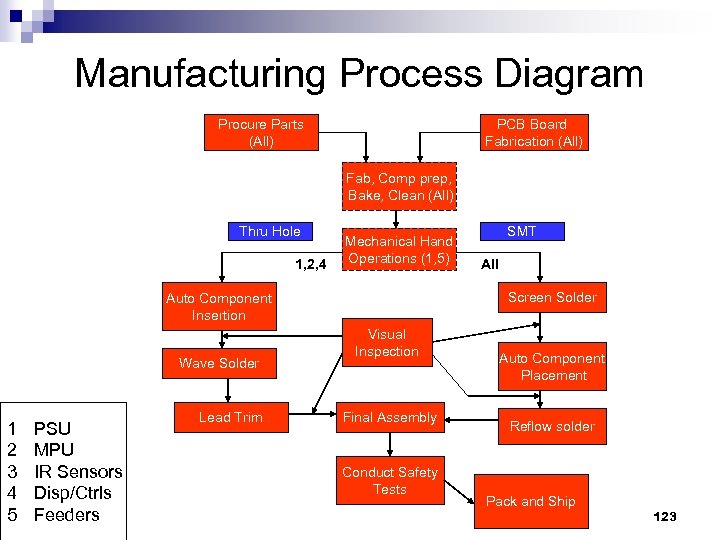
Manufacturing Process Diagram Procure Parts (All) PCB Board Fabrication (All) Fab, Comp prep, Bake, Clean (All) Thru Hole 1, 2, 4 Mechanical Hand Operations (1, 5) 1 2 3 4 5 PSU MPU IR Sensors Disp/Ctrls Feeders Lead Trim All Screen Solder Auto Component Insertion Wave Solder SMT Visual Inspection Final Assembly Conduct Safety Tests Auto Component Placement Reflow solder Pack and Ship 123
b07396b1da8ed6d0f82b9e33fc9778b4.ppt