4d9784cf34951d1f9fe71585806413a0.ppt
- Количество слайдов: 25
 Introduction to Nano-scale Mechanical Properties Testing Micro Materials Ltd. Wrexham, UK.
 Outline • Depth-sensing indentation • The Nano. Test system • Case studies • Nanoindentation – bond pads • Nano-impact – fatigue of DLC films • Polymer nanoindentation • Summary
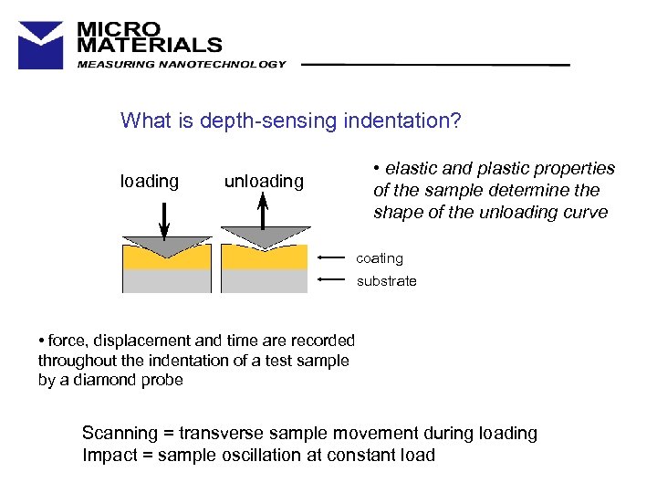 What is depth-sensing indentation? loading • elastic and plastic properties of the sample determine the shape of the unloading curve unloading coating substrate • force, displacement and time are recorded throughout the indentation of a test sample by a diamond probe Scanning = transverse sample movement during loading Impact = sample oscillation at constant load
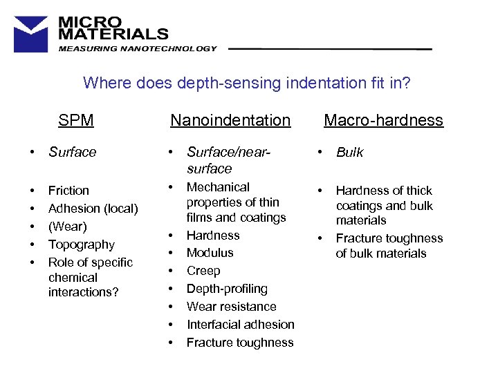 Where does depth-sensing indentation fit in? SPM Nanoindentation Macro-hardness • Surface/nearsurface • Bulk • • Friction Adhesion (local) (Wear) Topography Role of specific chemical interactions? • • Mechanical properties of thin films and coatings Hardness Modulus Creep Depth-profiling Wear resistance Interfacial adhesion Fracture toughness • Hardness of thick coatings and bulk materials Fracture toughness of bulk materials
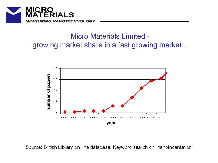 Micro Materials Limited growing market share in a fast growing market. . . Source: British Library on-line database. Keyword search on “nanoindentation”.
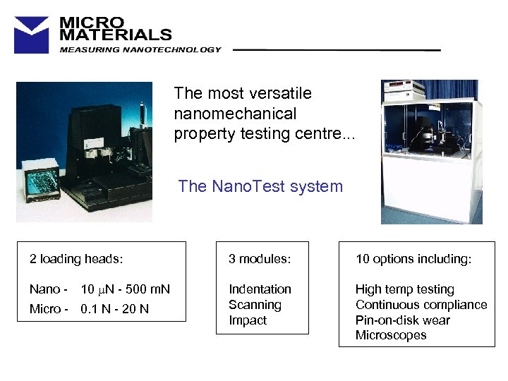 The most versatile nanomechanical property testing centre. . . The Nano. Test system 2 loading heads: Nano - 10 m. N - 500 m. N Micro - 0. 1 N - 20 N 3 modules: 10 options including: Indentation Scanning Impact High temp testing Continuous compliance Pin-on-disk wear Microscopes
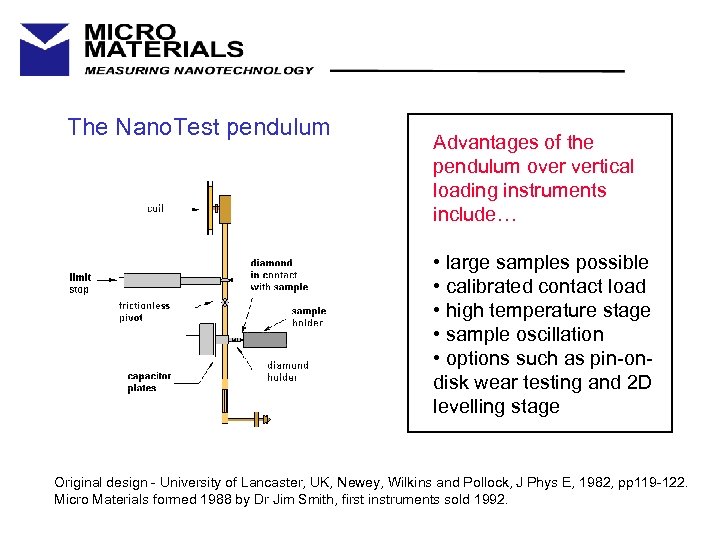 The Nano. Test pendulum Advantages of the pendulum over vertical loading instruments include… • large samples possible • calibrated contact load • high temperature stage • sample oscillation • options such as pin-ondisk wear testing and 2 D levelling stage Original design - University of Lancaster, UK, Newey, Wilkins and Pollock, J Phys E, 1982, pp 119 -122. Micro Materials formed 1988 by Dr Jim Smith, first instruments sold 1992.
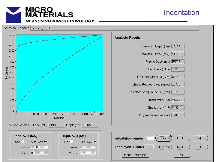
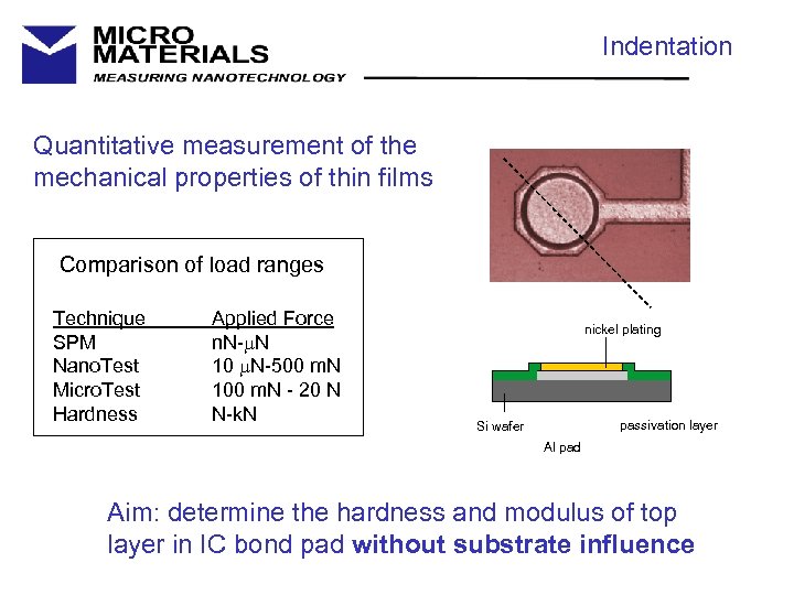 Indentation Quantitative measurement of the mechanical properties of thin films Comparison of load ranges Technique SPM Nano. Test Micro. Test Hardness Applied Force n. N-m. N 10 m. N-500 m. N 100 m. N - 20 N N-k. N nickel plating passivation layer Si wafer Al pad Aim: determine the hardness and modulus of top layer in IC bond pad without substrate influence
 Indentation Nano. Test indentation module Techniques • Nanoindentation • Microindentation • Load-partial-unload • High temperature testing • Continuous compliance Properties • Hardness • Elastic modulus • Fracture toughness • Adhesion • Creep • Elastic and plastic work • Elastic recovery parameter • Stress-strain
 Indentation
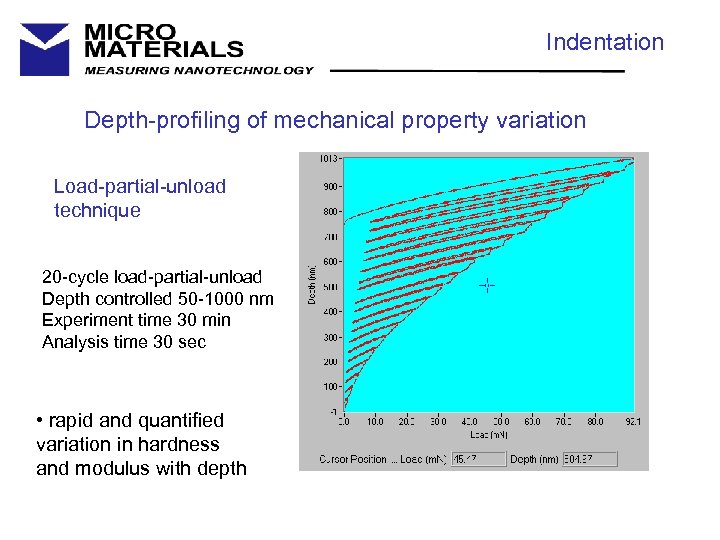 Indentation Depth-profiling of mechanical property variation Load-partial-unload technique 20 -cycle load-partial-unload Depth controlled 50 -1000 nm Experiment time 30 min Analysis time 30 sec • rapid and quantified variation in hardness and modulus with depth
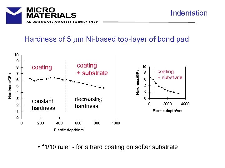 Indentation Hardness of 5 mm Ni-based top-layer of bond pad coating constant hardness coating + substrate decreasing hardness • “ 1/10 rule” - for a hard coating on softer substrate
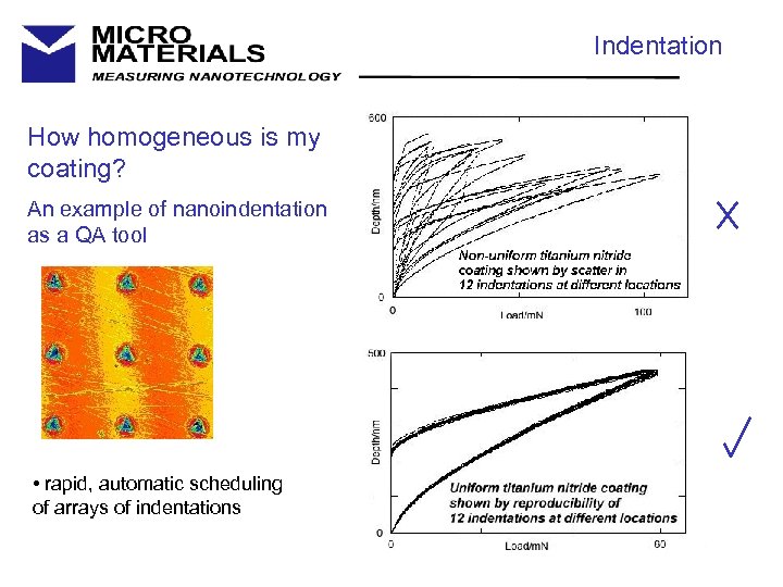 Indentation How homogeneous is my coating? An example of nanoindentation as a QA tool • rapid, automatic scheduling of arrays of indentations
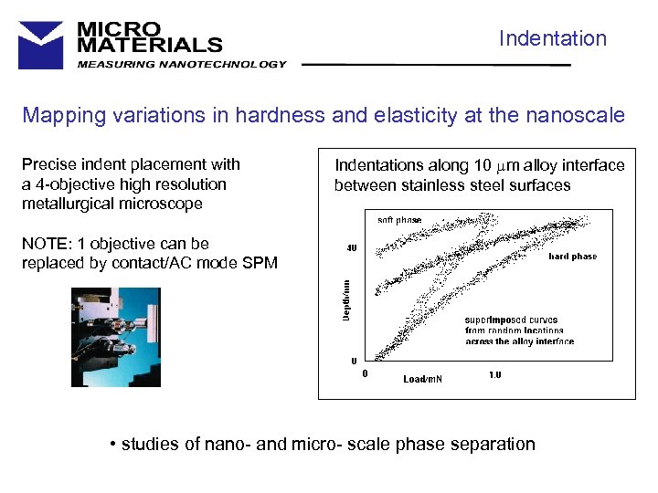 Indentation Mapping variations in hardness and elasticity at the nanoscale Precise indent placement with a 4 -objective high resolution metallurgical microscope Indentations along 10 mm alloy interface between stainless steel surfaces NOTE: 1 objective can be replaced by contact/AC mode SPM • studies of nano- and micro- scale phase separation
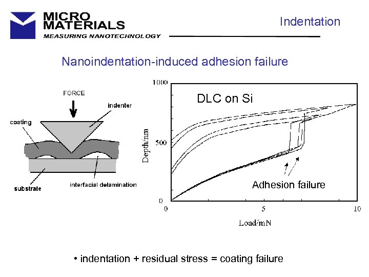 Indentation Nanoindentation-induced adhesion failure DLC on Si Adhesion failure • indentation + residual stress = coating failure
 Scanning Nano. Test scanning module for… • Scratch testing • Nano- and micro- friction • Adhesion • Profilometry • Acoustic Emission • Fatigue wear “Nanotribometer”
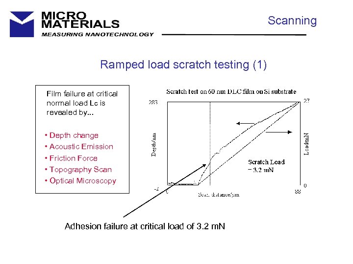 Scanning Ramped load scratch testing (1) Film failure at critical normal load Lc is revealed by. . . • Depth change • Acoustic Emission • Friction Force • Topography Scan • Optical Microscopy Adhesion failure at critical load of 3. 2 m. N
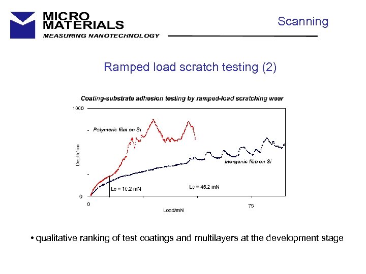 Scanning Ramped load scratch testing (2) • qualitative ranking of test coatings and multilayers at the development stage
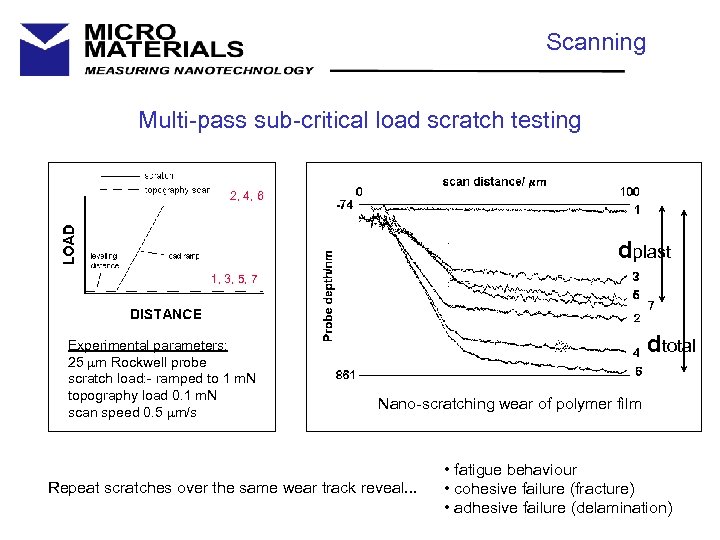 Scanning Multi-pass sub-critical load scratch testing 2, 4, 6 dplast 1, 3, 5, 7 Experimental parameters: 25 mm Rockwell probe scratch load: - ramped to 1 m. N topography load 0. 1 m. N scan speed 0. 5 mm/s dtotal Nano-scratching wear of polymer film Repeat scratches over the same wear track reveal. . . • fatigue behaviour • cohesive failure (fracture) • adhesive failure (delamination)
 Impact Nano. Test impact module for… • Impact testing • Contact fatigue testing • Erosive wear testing • Fracture toughness • Adhesion testing • Dynamic hardness The only commercial nano-impact tester available
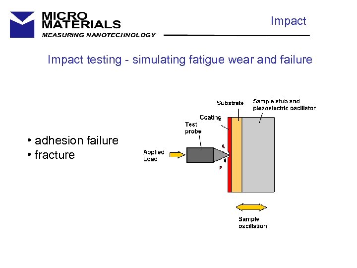 Impact testing - simulating fatigue wear and failure • adhesion failure • fracture
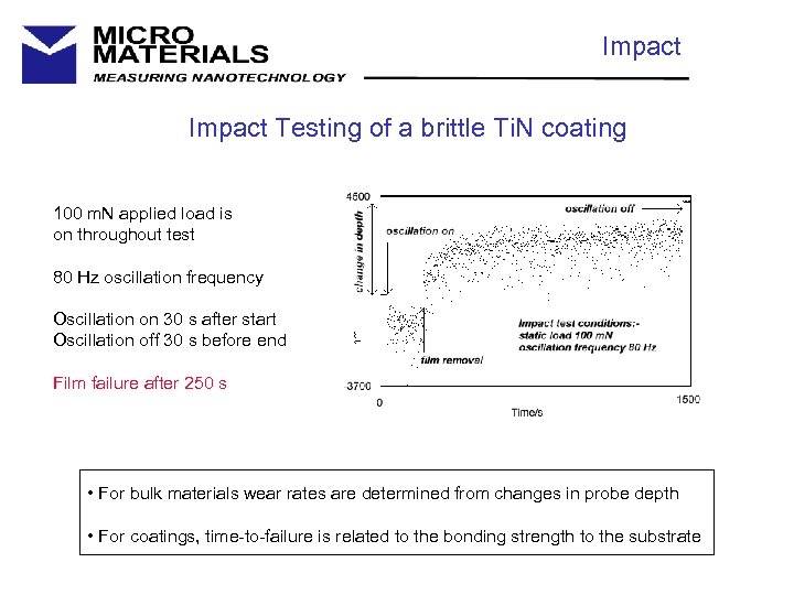 Impact Testing of a brittle Ti. N coating 100 m. N applied load is on throughout test 80 Hz oscillation frequency Oscillation on 30 s after start Oscillation off 30 s before end Film failure after 250 s • For bulk materials wear rates are determined from changes in probe depth • For coatings, time-to-failure is related to the bonding strength to the substrate
 To summarise…. 1. Nanoindentation techniques are essential in the optimisation of the mechanical properties of thin films and coatings 2. The Nano. Test has large range of testing techniques, and therefore offers a complete testing capability 3. These techniques are possible due to the unique pendulum design 4. The high temperature option and impact module allow testing under contact conditions that can closely simulate those in service 5. The versatility and wide range of options have resulted in the system finding applications in….
 Nano. Test systems are in regular use in… MIT USA Eastman Kodak USA Philips Netherlands HP Singapore Gintic Singapore Cambridge Uni UK Barcelona Uni Spain VITO Belgium NPL UK Enterprise Ireland Salford Uni UK Cranfield Uni UK Timken USA RPI NY USA AGFA DE LOT Oriel DE Paisley UK Loughborough UK TU Clausthal DE UMIST UK DERA UK Leeds Uni UK ICM Madrid Spain Trivandrum India . . . and many more - over 75 sites worldwide
 Current Nano. Test application areas include… • • • Automotive Bearings Biomedical Devices Ceramics Composites Contact Lenses Cutting Tools Hard Coatings Laminates Magnetic Disks Microelectronics Optical Coatings • • • Optical Disks Packaging Materials Paints Paper Coatings Pharmaceuticals Photographic Film Polymers Powders Printing Plates Semiconductors Thin Film Adhesion Turbine Blades . . . future application areas will be in?


