cbcaf311124ef5c36625e09fa2dd7cc2.ppt
- Количество слайдов: 53
 Introduction to Digital Design with VHDL © A. Schöning/V. Angelov physi. uni-heidelberg. de IRTG 2010 Heidelberg 1
 Topics • • Why digital processing? Basic elements and ideas Combinational circuits VHDL introduction Circuits with memory Simulating with VHDL Technologies – FPGA, ASIC… Some practical exercises © A. Schöning/V. Angelov physi. uni-heidelberg. de IRTG 2010 Heidelberg 2
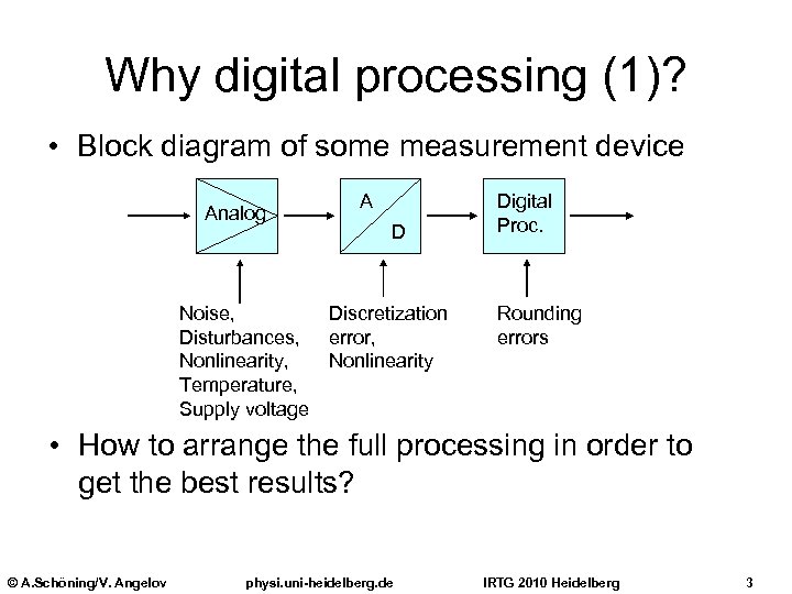 Why digital processing (1)? • Block diagram of some measurement device Analog Noise, Disturbances, Nonlinearity, Temperature, Supply voltage A D Discretization error, Nonlinearity Digital Proc. Rounding errors • How to arrange the full processing in order to get the best results? © A. Schöning/V. Angelov physi. uni-heidelberg. de IRTG 2010 Heidelberg 3
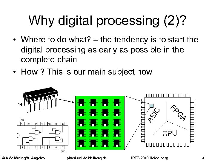 Why digital processing (2)? • Where to do what? – the tendency is to start the digital processing as early as possible in the complete chain • How ? This is our main subject now FP AS IC G A CPU © A. Schöning/V. Angelov physi. uni-heidelberg. de IRTG 2010 Heidelberg 4
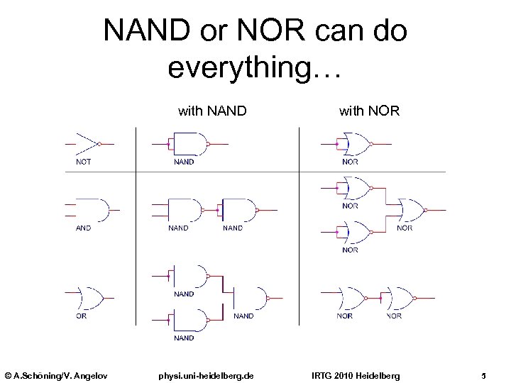 NAND or NOR can do everything… with NAND © A. Schöning/V. Angelov physi. uni-heidelberg. de with NOR IRTG 2010 Heidelberg 5
 What kind of logical elements do we need? • Exactly like a house, that can be built using many identical small bricks, one logical circuit can be built using many identical NOR (ORNOT) or NAND (AND-NOT) elements • For practical reasons it is much better to have a rich set of different logical elements, this will save area and power and will speed up the circuit © A. Schöning/V. Angelov physi. uni-heidelberg. de IRTG 2010 Heidelberg 6
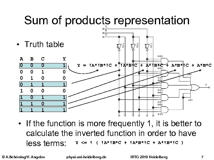 Sum of products representation • Truth table A 0 0 1 1 B 0 0 1 1 C 0 1 0 1 Y 1 0 0 1 1 1 Y = !A*!B*!C + !A*B*C + A*!B*C + A*B*!C + A*B*C • If the function is more frequently 1, it is better to calculate the inverted function in order to have less terms: Y <= ! ( !A*!B*C + !A*B*!C + A*!B*!C ) © A. Schöning/V. Angelov physi. uni-heidelberg. de IRTG 2010 Heidelberg 7
 Conclusions(1) – PAL/CPLD/HDL • The sum of products representation was a good move! It seems to be a universal method (with some exceptions) to build any logical function – PAL and CPLD • Drawing of the circuit is tedious and not very reliable! • Writing of equations seems to be easier and more reliable → languages to describe hardware (HDL - hardware description language) © A. Schöning/V. Angelov physi. uni-heidelberg. de IRTG 2010 Heidelberg 8
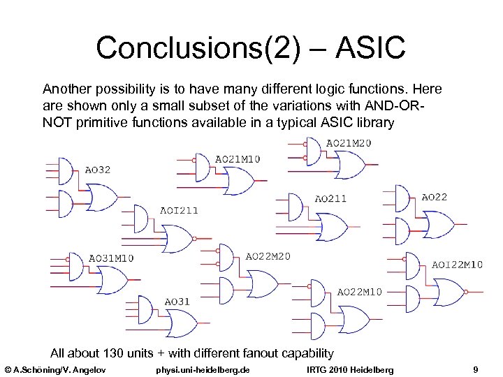 Conclusions(2) – ASIC Another possibility is to have many different logic functions. Here are shown only a small subset of the variations with AND-ORNOT primitive functions available in a typical ASIC library All about 130 units + with different fanout capability © A. Schöning/V. Angelov physi. uni-heidelberg. de IRTG 2010 Heidelberg 9
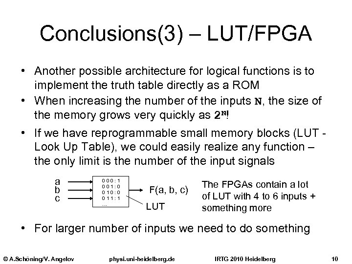 Conclusions(3) – LUT/FPGA • Another possible architecture for logical functions is to implement the truth table directly as a ROM • When increasing the number of the inputs N, the size of the memory grows very quickly as 2 N! • If we have reprogrammable small memory blocks (LUT Look Up Table), we could easily realize any function – the only limit is the number of the input signals a b c 000: 1 001: 0 010: 0 011: 1 … F(a, b, c) LUT The FPGAs contain a lot of LUT with 4 to 6 inputs + something more • For larger number of inputs we need to do something © A. Schöning/V. Angelov physi. uni-heidelberg. de IRTG 2010 Heidelberg 10
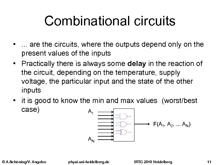 Combinational circuits • . . . are the circuits, where the outputs depend only on the present values of the inputs • Practically there is always some delay in the reaction of the circuit, depending on the temperature, supply voltage, the particular input and the state of the other inputs • it is good to know the min and max values (worst/best case) A 1 F(A 1, A 2, . . . AN) AN © A. Schöning/V. Angelov physi. uni-heidelberg. de IRTG 2010 Heidelberg 11
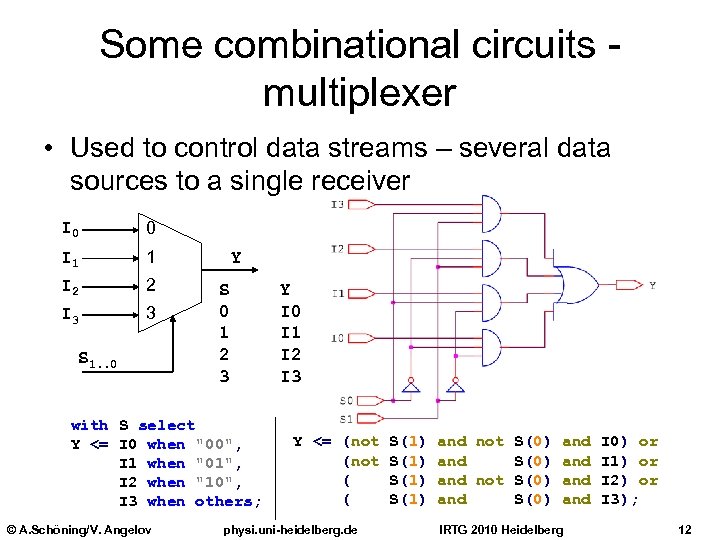 Some combinational circuits multiplexer • Used to control data streams – several data sources to a single receiver I 0 0 I 1 1 I 2 2 I 3 3 S 1. . 0 Y S 0 1 2 3 with S select Y <= I 0 when "00", I 1 when "01", I 2 when "10", I 3 when others; © A. Schöning/V. Angelov Y I 0 I 1 I 2 I 3 Y <= (not ( ( physi. uni-heidelberg. de S(1) and not S(0) and I 0) or and S(0) and I 1) or and not S(0) and I 2) or and S(0) and I 3); IRTG 2010 Heidelberg 12
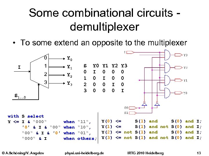 Some combinational circuits demultiplexer • To some extend an opposite to the multiplexer 0 1 Y 1 2 Y 2 3 I Y 0 Y 3 S 1. . 0 with S select Y <= I & "000" '0' & I & "00" & I & '0' "000" & I © A. Schöning/V. Angelov when S 0 1 2 3 Y 0 I 0 0 0 "11", "10", "01", others; Y 1 0 I 0 0 Y 2 0 0 I 0 Y(0) Y(1) Y(2) Y(3) physi. uni-heidelberg. de Y 3 0 0 0 I <= S(1) <= not S(1) and S(0) and and not S(0) and IRTG 2010 Heidelberg I; I; 13
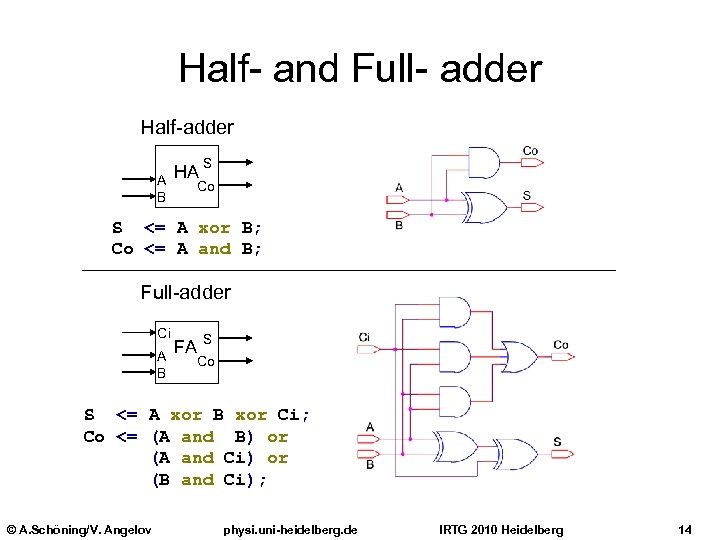 Half- and Full- adder Half-adder A B HA S Co S <= A xor B; Co <= A and B; Full-adder Ci A B FA S Co S <= A xor B xor Ci; Co <= (A and B) or (A and Ci) or (B and Ci); © A. Schöning/V. Angelov physi. uni-heidelberg. de IRTG 2010 Heidelberg 14
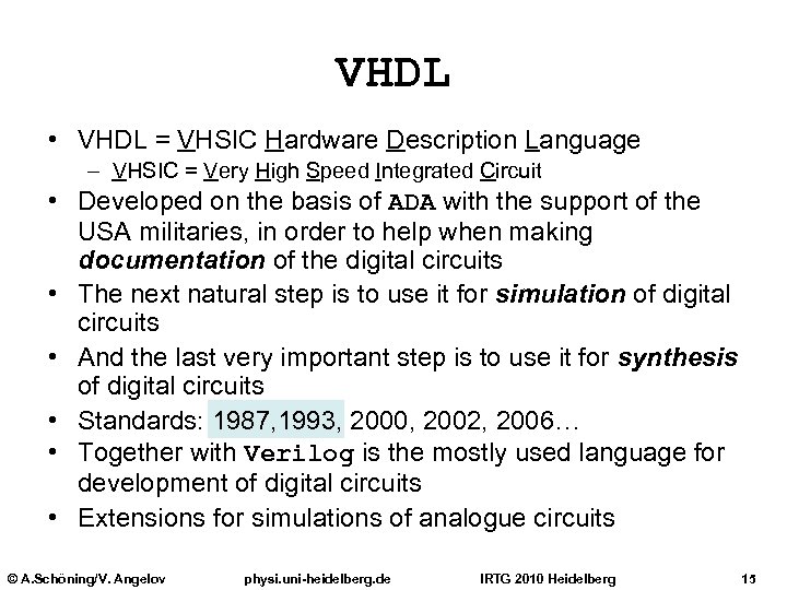 VHDL • VHDL = VHSIC Hardware Description Language – VHSIC = Very High Speed Integrated Circuit • Developed on the basis of ADA with the support of the USA militaries, in order to help when making documentation of the digital circuits • The next natural step is to use it for simulation of digital circuits • And the last very important step is to use it for synthesis of digital circuits • Standards: 1987, 1993, 2000, 2002, 2006… • Together with Verilog is the mostly used language for development of digital circuits • Extensions for simulations of analogue circuits © A. Schöning/V. Angelov physi. uni-heidelberg. de IRTG 2010 Heidelberg 15
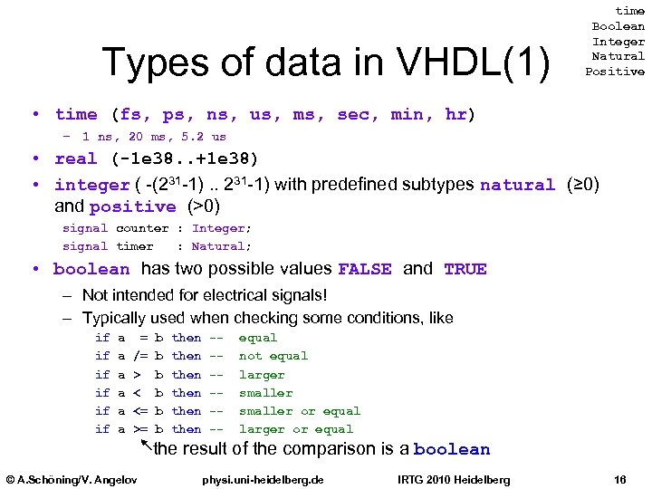 Types of data in VHDL(1) time Boolean Integer Natural Positive • time (fs, ps, ns, us, ms, sec, min, hr) – 1 ns, 20 ms, 5. 2 us • real (-1 e 38. . +1 e 38) • integer ( -(231 -1). . 231 -1) with predefined subtypes natural (≥ 0) and positive (>0) signal counter : Integer; signal timer : Natural; • boolean has two possible values FALSE and TRUE – Not intended for electrical signals! – Typically used when checking some conditions, like if if if a a a = /= > < <= >= b b b then then ------- equal not equal larger smaller or equal larger or equal the result of the comparison is a boolean © A. Schöning/V. Angelov physi. uni-heidelberg. de IRTG 2010 Heidelberg 16
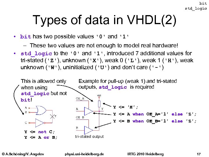 bit std_logic Types of data in VHDL(2) • bit has two possible values '0' and '1' – These two values are not enough to model real hardware! • std_logic to the '0' and '1', introduced 7 additional values for tri-stated ('Z'), unknown ('X'), weak 0 ('L'), weak 1 ('H'), weak unknown ('W'), uninitialized ('U') and don‘t care ('-') This is allowed only when using std_logic but not bit! Example for pull-up (weak 1) and tri-stated outputs, std_logic is required Y <= 'H'; Y <= A when OE_A='1' else 'Z'; Y <= B when OE_B='1' else 'Z'; Y <= not C; Y <= A or B; © A. Schöning/V. Angelov tri-stated output physi. uni-heidelberg. de IRTG 2010 Heidelberg 17
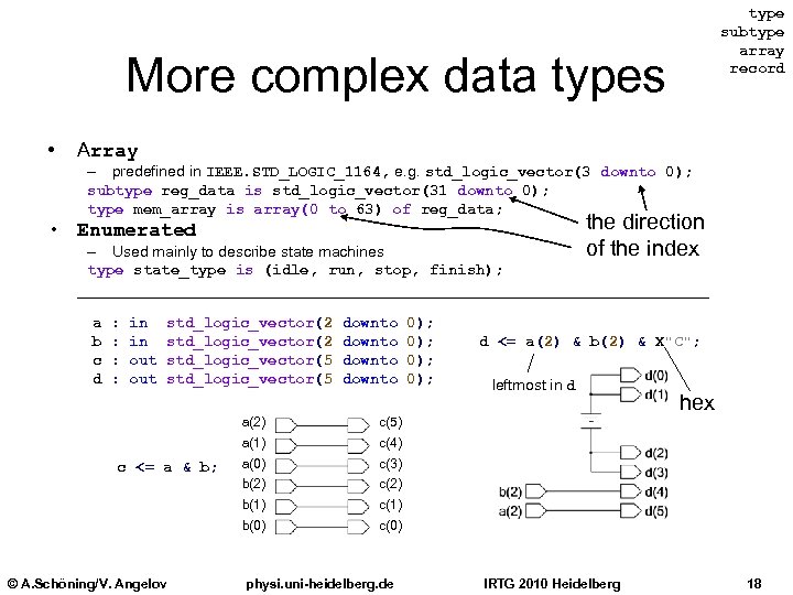 type subtype array record More complex data types • Array – predefined in IEEE. STD_LOGIC_1164, e. g. std_logic_vector(3 downto 0); subtype reg_data is std_logic_vector(31 downto 0); type mem_array is array(0 to 63) of reg_data; • Enumerated – Used mainly to describe state machines type state_type is (idle, run, stop, finish); a b c d : : in in out std_logic_vector(2 std_logic_vector(5 downto a(2) c(1) b(0) hex c(3) b(1) © A. Schöning/V. Angelov a(0) leftmost in d c(4) b(2) c <= a & b; d <= a(2) & b(2) & X"C"; c(5) a(1) 0); 0); the direction of the index c(0) physi. uni-heidelberg. de IRTG 2010 Heidelberg 18
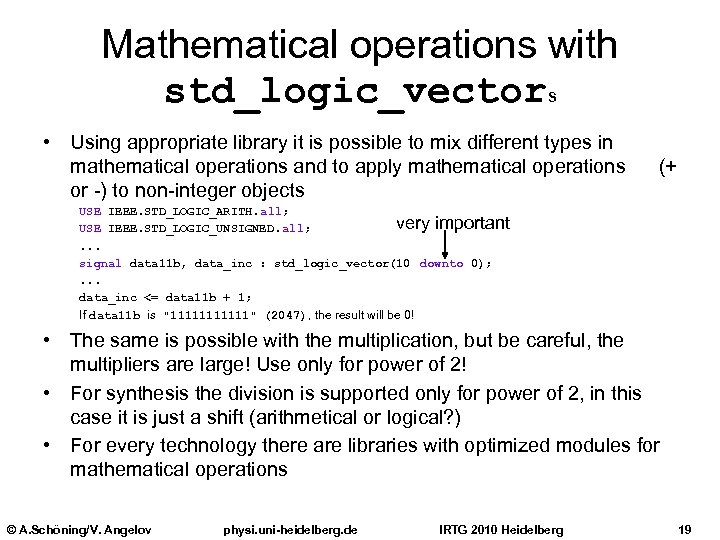 Mathematical operations with std_logic_vectors • Using appropriate library it is possible to mix different types in mathematical operations and to apply mathematical operations or -) to non-integer objects (+ USE IEEE. STD_LOGIC_ARITH. all; very important USE IEEE. STD_LOGIC_UNSIGNED. all; . . . signal data 11 b, data_inc : std_logic_vector(10 downto 0); . . . data_inc <= data 11 b + 1; If data 11 b is "111111" (2047), the result will be 0! • The same is possible with the multiplication, but be careful, the multipliers are large! Use only for power of 2! • For synthesis the division is supported only for power of 2, in this case it is just a shift (arithmetical or logical? ) • For every technology there are libraries with optimized modules for mathematical operations © A. Schöning/V. Angelov physi. uni-heidelberg. de IRTG 2010 Heidelberg 19
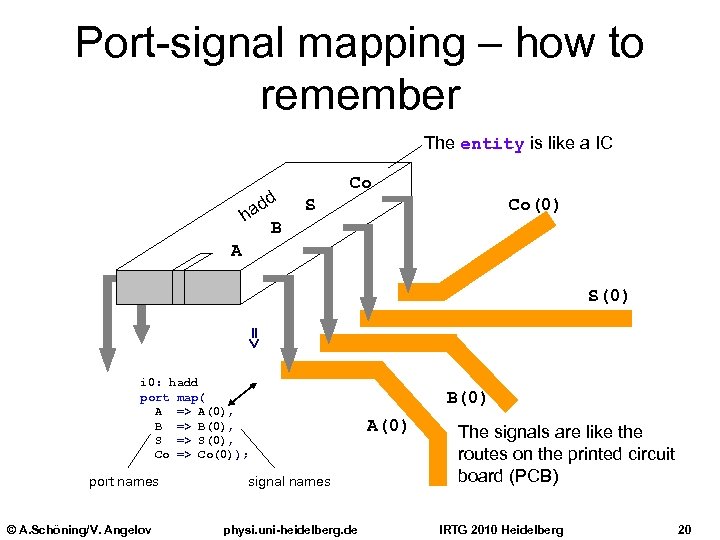 Port-signal mapping – how to remember The entity is like a IC d ad h B Co Co(0) S A S(0) => i 0: hadd port map( A => A(0), B => B(0), S => S(0), Co => Co(0)); port names © A. Schöning/V. Angelov signal names physi. uni-heidelberg. de B(0) A(0) The signals are like the routes on the printed circuit board (PCB) IRTG 2010 Heidelberg 20
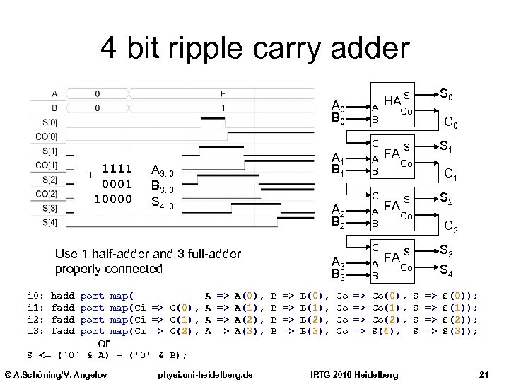 4 bit ripple carry adder A 0 B 0 A B Ci 1111 + 0001 10000 A 1 B 1 A 3. . 0 B 3. . 0 S 4. . 0 Ci A 2 B 2 hadd fadd port or map( A map(Ci => C(0), A map(Ci => C(1), A map(Ci => C(2), A => => A(0), A(1), A(2), A(3), A B Ci Use 1 half-adder and 3 full-adder properly connected i 0: i 1: i 2: i 3: A B A 3 B B B B => => B(0), B(1), B(2), B(3), Co Co A B => => HA S 0 S Co FA C 0 S 1 S Co FA C 1 S 2 S Co C 2 S S 3 Co S 4 FA Co(0), Co(1), Co(2), S(4), S S => => S(0)); S(1)); S(2)); S(3)); S <= ('0' & A) + ('0' & B); © A. Schöning/V. Angelov physi. uni-heidelberg. de IRTG 2010 Heidelberg 21
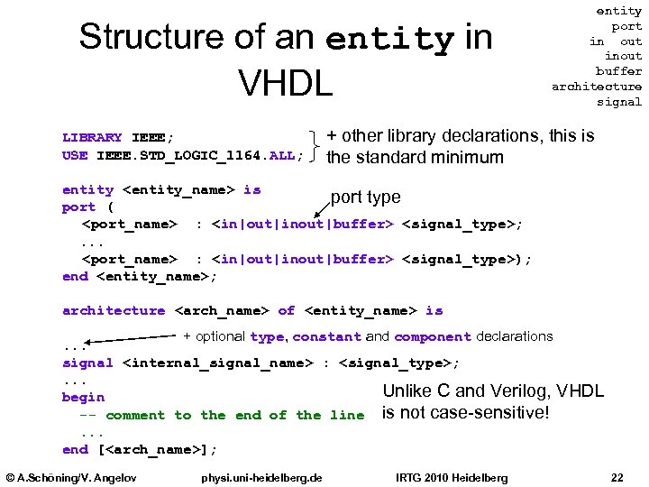 Structure of an entity in VHDL LIBRARY IEEE; USE IEEE. STD_LOGIC_1164. ALL; entity port in out inout buffer architecture signal + other library declarations, this is the standard minimum entity
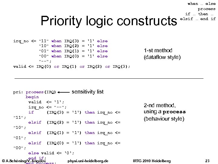 Priority logic constructs irq_no <= "11" when IRQ(3) = "10" when IRQ(2) = "01" when IRQ(1) = "00" when IRQ(0) = "--"; valid <= IRQ(0) or IRQ(1) or '1' '1' 1 -st method (dataflow style) IRQ(2) or IRQ(3); pri: process(IRQ) sensitivity begin valid <= '1'; irq_no <= "--"; if (IRQ(3) = '1') then "11"; elsif (IRQ(2) = '1') then "10"; elsif (IRQ(1) = '1') then "01"; elsif (IRQ(0) = '1') then "00"; else valid <= '0'; end if; © A. Schöning/V. Angelov else when … else process if … then … elsif … end if list irq_no <= 2 -nd method, using a process (behaviour style) irq_no <= physi. uni-heidelberg. de IRTG 2010 Heidelberg 23
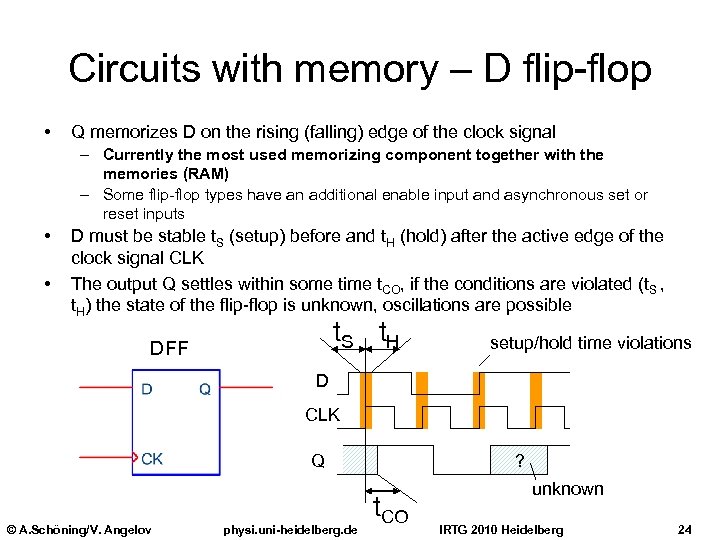 Circuits with memory – D flip-flop • Q memorizes D on the rising (falling) edge of the clock signal – Currently the most used memorizing component together with the memories (RAM) – Some flip-flop types have an additional enable input and asynchronous set or reset inputs • • D must be stable t. S (setup) before and t. H (hold) after the active edge of the clock signal CLK The output Q settles within some time t. CO, if the conditions are violated (t. S , t. H) the state of the flip-flop is unknown, oscillations are possible t. S t. H DFF setup/hold time violations D CLK Q © A. Schöning/V. Angelov physi. uni-heidelberg. de ? t. CO unknown IRTG 2010 Heidelberg 24
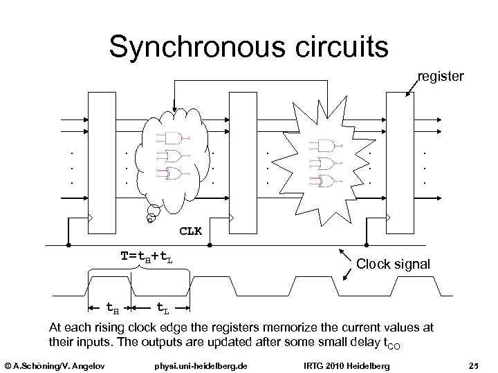 Synchronous circuits register . . . . CLK T=t. H+t. L t. H Clock signal t. L At each rising clock edge the registers memorize the current values at their inputs. The outputs are updated after some small delay t. CO © A. Schöning/V. Angelov physi. uni-heidelberg. de IRTG 2010 Heidelberg 25
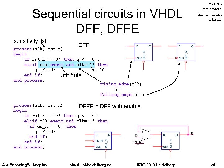 Sequential circuits in VHDL DFF, DFFE sensitivity list event process if … then elsif DFF process(clk, rst_n) begin if rst_n = '0' then q <= '0'; elsif clk'event and clk='1' then q <= d; or '0' end if; attribute end process; rising_edge(clk) or falling_edge(clk) process(clk, rst_n) DFFE = DFF begin if rst_n = '0' then q <= '0'; elsif clk'event and clk='1' then if en_n = '0' then q <= d; end if; end process; © A. Schöning/V. Angelov physi. uni-heidelberg. de with enable = IRTG 2010 Heidelberg 26
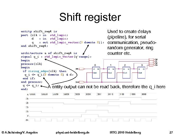 Shift register entity shift_reg 4 is port (clk : in std_logic; d : in std_logic; q : out std_logic_vector(3 downto 0)); end shift_reg 4; architecture a of shift_reg 4 is signal q_i : std_logic_vector(q'range); begin process(clk) 0 begin if rising_edge(clk) then q_i <= q_i(2 downto 0) & d; end if; end process; q <= q_i; A entity output can not be end; © A. Schöning/V. Angelov physi. uni-heidelberg. de Used to create delays (pipeline), for serial communication, pseudorandom generator, ring counter etc. 1 2 3 read back, therefore the q_i here IRTG 2010 Heidelberg 27
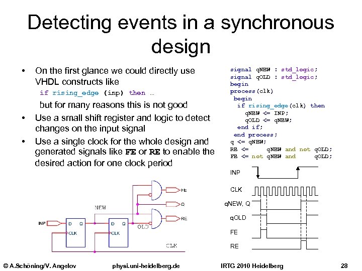 Detecting events in a synchronous design • On the first glance we could directly use VHDL constructs like if rising_edge (inp) then … • • but for many reasons this is not good Use a small shift register and logic to detect changes on the input signal Use a single clock for the whole design and generated signals like FE or RE to enable the desired action for one clock period signal q. NEW : std_logic; signal q. OLD : std_logic; begin process(clk) begin if rising_edge(clk) then q. NEW <= INP; q. OLD <= q. NEW; end if; end process; q <= q. NEW; RE <= q. NEW and not q. OLD; FE <= not q. NEW and q. OLD; INP CLK q. NEW, Q q. OLD FE RE © A. Schöning/V. Angelov physi. uni-heidelberg. de IRTG 2010 Heidelberg 28
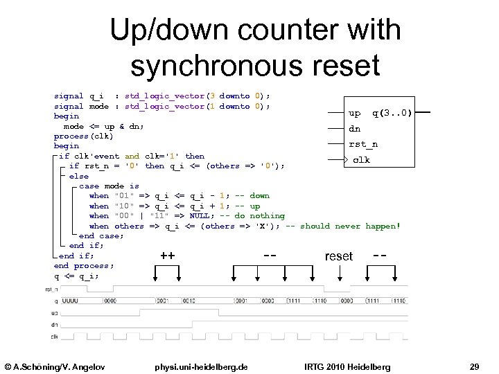 Up/down counter with synchronous reset signal q_i : std_logic_vector(3 downto 0); signal mode : std_logic_vector(1 downto 0); up q(3. . 0) begin mode <= up & dn; dn process(clk) rst_n begin if clk'event and clk='1' then clk if rst_n = '0' then q_i <= (others => '0'); else case mode is when "01" => q_i <= q_i - 1; -- down when "10" => q_i <= q_i + 1; -- up when "00" | "11" => NULL; -- do nothing when others => q_i <= (others => 'X'); -- should never happen! end case; end if; ++ --reset end process; q <= q_i; © A. Schöning/V. Angelov physi. uni-heidelberg. de IRTG 2010 Heidelberg 29
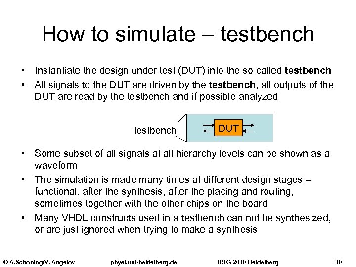 How to simulate – testbench • Instantiate the design under test (DUT) into the so called testbench • All signals to the DUT are driven by the testbench, all outputs of the DUT are read by the testbench and if possible analyzed testbench DUT • Some subset of all signals at all hierarchy levels can be shown as a waveform • The simulation is made many times at different design stages – functional, after the synthesis, after the placing and routing, sometimes together with the other chips on the board • Many VHDL constructs used in a testbench can not be synthesized, or are just ignored when trying to make a synthesis © A. Schöning/V. Angelov physi. uni-heidelberg. de IRTG 2010 Heidelberg 30
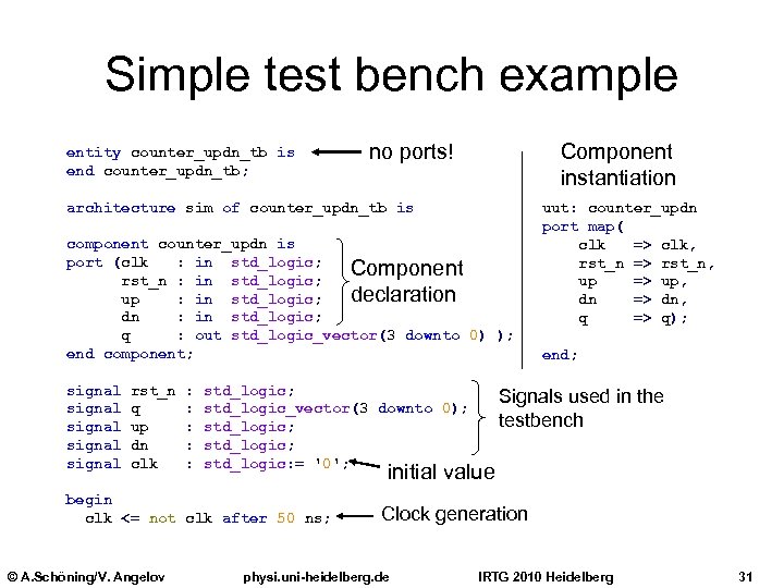 Simple test bench example entity counter_updn_tb is end counter_updn_tb; no ports! Component instantiation architecture sim of counter_updn_tb is component counter_updn is port (clk : in std_logic; Component rst_n : in std_logic; declaration up : in std_logic; dn : in std_logic; q : out std_logic_vector(3 downto 0) ); end component; signal signal rst_n q up dn clk : : : std_logic; std_logic_vector(3 downto 0); std_logic; std_logic: = '0'; end; Signals used in the testbench initial value begin clk <= not clk after 50 ns; © A. Schöning/V. Angelov uut: counter_updn port map( clk => clk, rst_n => rst_n, up => up, dn => dn, q => q); Clock generation physi. uni-heidelberg. de IRTG 2010 Heidelberg 31
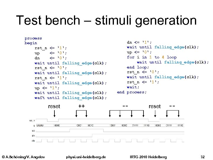 Test bench – stimuli generation process begin rst_n <= '1'; up <= '0'; dn <= '0'; wait until falling_edge(clk); rst_n <= '1'; wait until falling_edge(clk); up <= '1'; wait until falling_edge(clk); reset © A. Schöning/V. Angelov ++ physi. uni-heidelberg. de dn <= '1'; wait until falling_edge(clk); up <= '0'; for i in 1 to 4 loop wait until falling_edge(clk); end loop; rst_n <= '0'; wait until falling_edge(clk); rst_n <= '1'; wait; end process; -- reset IRTG 2010 Heidelberg -- 32
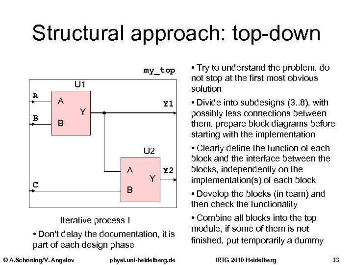 Structural approach: top-down my_top U 1 A B A Y 1 Y B U 2 A C Y Y 2 B Iterative process ! • Don't delay the documentation, it is part of each design phase © A. Schöning/V. Angelov physi. uni-heidelberg. de • Try to understand the problem, do not stop at the first most obvious solution • Divide into subdesigns (3. . 8), with possibly less connections between them, prepare block diagrams before starting with the implementation • Clearly define the function of each block and the interface between the blocks, independently on the implementation(s) of each block • Develop the blocks (in team) and then check the functionality • Combine all blocks into the top module, if some of them is not finished, put temporarily a dummy IRTG 2010 Heidelberg 33
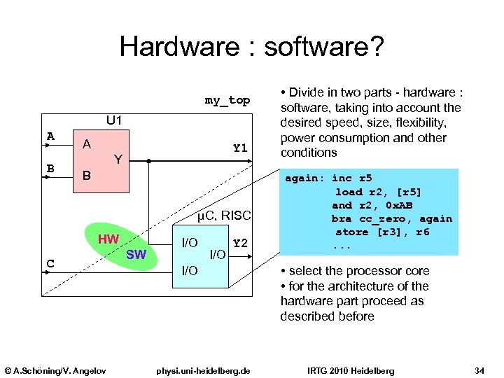 Hardware : software? my_top U 1 A B A Y 1 Y B μC, RISC HW C © A. Schöning/V. Angelov SW I/O Y 2 I/O physi. uni-heidelberg. de • Divide in two parts - hardware : software, taking into account the desired speed, size, flexibility, power consumption and other conditions again: inc r 5 load r 2, [r 5] and r 2, 0 x. AB bra cc_zero, again store [r 3], r 6. . . • select the processor core • for the architecture of the hardware part proceed as described before IRTG 2010 Heidelberg 34
 Technologies © A. Schöning/V. Angelov physi. uni-heidelberg. de IRTG 2010 Heidelberg 35
 Integration scales & technologies • Small Scale Integration (SSI) ICs (74 xx, 4000) • Simple Programmable Logic Devices (SPLD) - PAL (Programmable Array Logic) & GAL (Generic Array Logic), Complex Programmable Logic Devices (CPLD) – Architecture, manufacturers, overview of the available products • Field Programmable Gate Arrays (FPGA) – Architecture, manufacturers, overview of the available products – Design flow FPGA/CPLD • Application Specific Integrated Circuits (ASIC) © A. Schöning/V. Angelov physi. uni-heidelberg. de IRTG 2010 Heidelberg 36
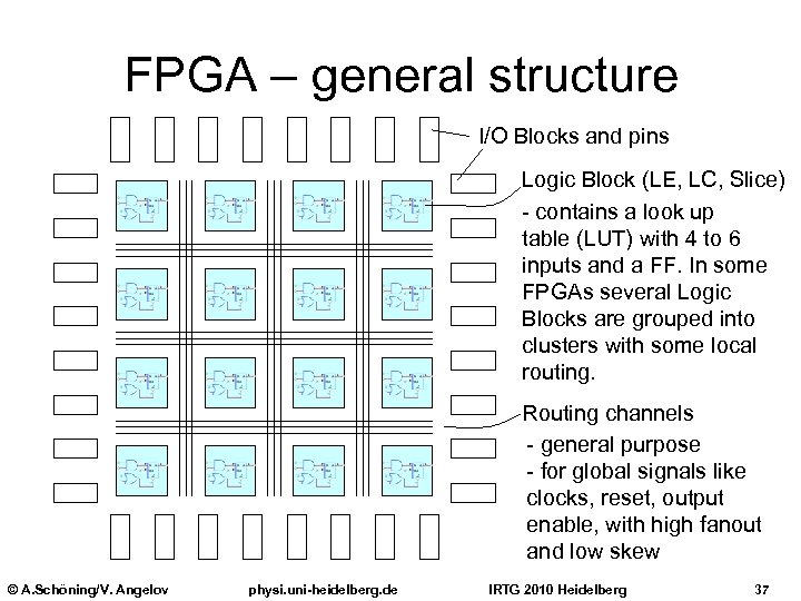 FPGA – general structure I/O Blocks and pins Logic Block (LE, LC, Slice) - contains a look up table (LUT) with 4 to 6 inputs and a FF. In some FPGAs several Logic Blocks are grouped into clusters with some local routing. Routing channels - general purpose - for global signals like clocks, reset, output enable, with high fanout and low skew © A. Schöning/V. Angelov physi. uni-heidelberg. de IRTG 2010 Heidelberg 37
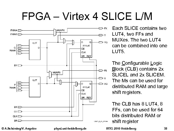 FPGA – Virtex 4 SLICE L/M Each SLICE contains two LUT 4, two FFs and MUXes. The two LUT 4 can be combined into one LUT 5. The Configurable Logic Block (CLB) contains 2 x SLICEL and 2 x SLICEM. The Ms can be used for distributed RAM and large shift registers. The CLB has 8 LUT 4, 8 FFs, can be used for 64 bits distributed RAM or shift register © A. Schöning/V. Angelov physi. uni-heidelberg. de IRTG 2010 Heidelberg 38
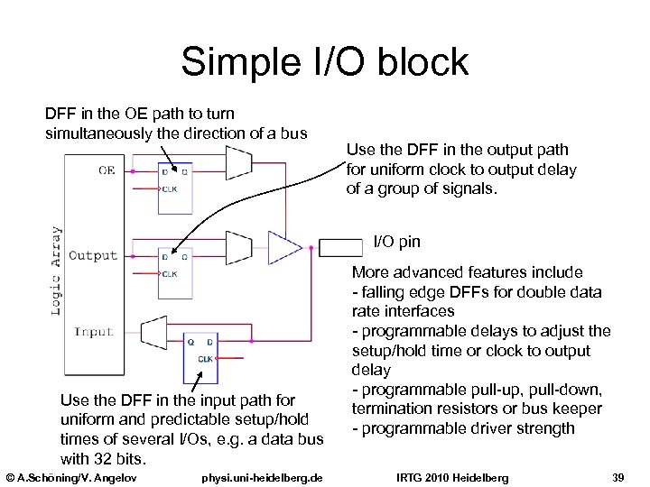 Simple I/O block DFF in the OE path to turn simultaneously the direction of a bus Use the DFF in the output path for uniform clock to output delay of a group of signals. I/O pin Use the DFF in the input path for uniform and predictable setup/hold times of several I/Os, e. g. a data bus with 32 bits. © A. Schöning/V. Angelov physi. uni-heidelberg. de More advanced features include - falling edge DFFs for double data rate interfaces - programmable delays to adjust the setup/hold time or clock to output delay - programmable pull-up, pull-down, termination resistors or bus keeper - programmable driver strength IRTG 2010 Heidelberg 39
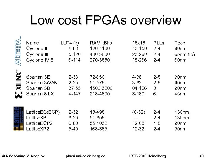 Low cost FPGAs overview Name Cyclone III Cyclone IV E LUT 4 (k) 4 -68 5 -120 6 -114 RAM k. Bits 120 -1100 400 -3800 270 -3880 18 x 18 13 -150 23 -288 15 -266 PLLs 2 -4 2 -4 Tech 90 nm 65 nm (lp) 60 nm Spartan 3 E Spartan 3 A/AN Spartan 3 D Spartan 6 LX 2 -33 2 -25 37 -53 4 -147 72 -650 54 -576 1500 -3200 216 -4800 4 -36 3 -32 84 -126 8 -180 2 -8 8 6 90 nm 45 nm Lattice. EC(ECP) Lattice. XP Lattice. ECP 2 Lattice. XP 2 2 -32 3 -20 6 -68 5 -40 18 -498 54 -396 55 -1032 166 -885 (0 -32) --12 -88 12 -32 2 -4 4 -8 2 -4 130 nm 90 nm © A. Schöning/V. Angelov physi. uni-heidelberg. de IRTG 2010 Heidelberg 40
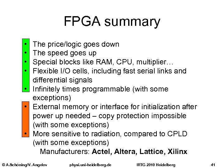 FPGA summary • • The price/logic goes down The speed goes up Special blocks like RAM, CPU, multiplier… Flexible I/O cells, including fast serial links and differential signals • Infinitely times programmable (with some exceptions) • External memory or interface for initialization after power up needed – copy protection impossible (with some exceptions) • More sensitive to radiation, compared to CPLD (with some exceptions) Manufacturers: Actel, Altera, Lattice, Xilinx © A. Schöning/V. Angelov physi. uni-heidelberg. de IRTG 2010 Heidelberg 41
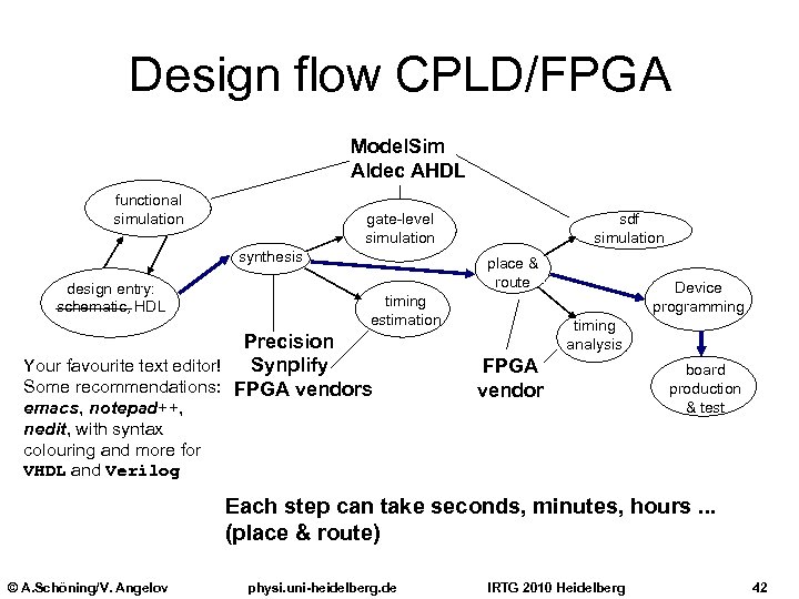 Design flow CPLD/FPGA Model. Sim Aldec AHDL functional simulation gate-level simulation synthesis design entry: schematic, HDL sdf simulation place & route timing estimation Precision Your favourite text editor! Synplify Some recommendations: FPGA vendors emacs, notepad++, nedit, with syntax colouring and more for VHDL and Verilog Device programming timing analysis FPGA vendor board production & test Each step can take seconds, minutes, hours. . . (place & route) © A. Schöning/V. Angelov physi. uni-heidelberg. de IRTG 2010 Heidelberg 42
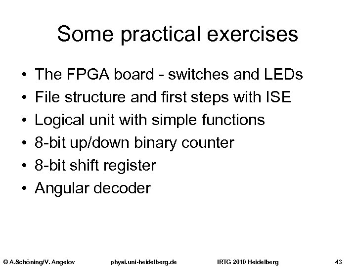 Some practical exercises • • • The FPGA board - switches and LEDs File structure and first steps with ISE Logical unit with simple functions 8 -bit up/down binary counter 8 -bit shift register Angular decoder © A. Schöning/V. Angelov physi. uni-heidelberg. de IRTG 2010 Heidelberg 43
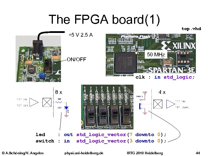 The FPGA board(1) top. vhd +5 V 2. 5 A ON/OFF 50 MHz clk : in std_logic; 8 x 4 x led : out std_logic_vector(7 downto 0); switch : in std_logic_vector(3 downto 0); © A. Schöning/V. Angelov physi. uni-heidelberg. de IRTG 2010 Heidelberg 44
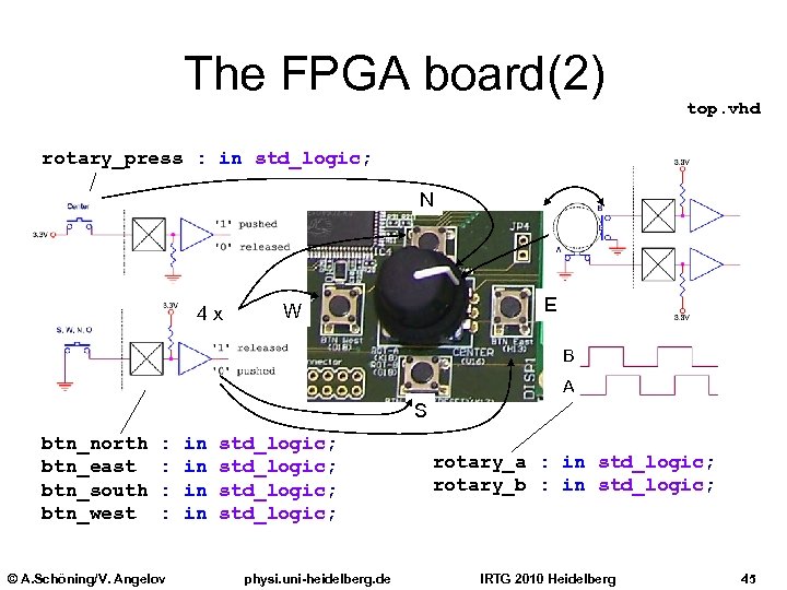 The FPGA board(2) top. vhd rotary_press : in std_logic; N 4 x E W B A S btn_north btn_east btn_south btn_west : : © A. Schöning/V. Angelov in in std_logic; physi. uni-heidelberg. de rotary_a : in std_logic; rotary_b : in std_logic; IRTG 2010 Heidelberg 45
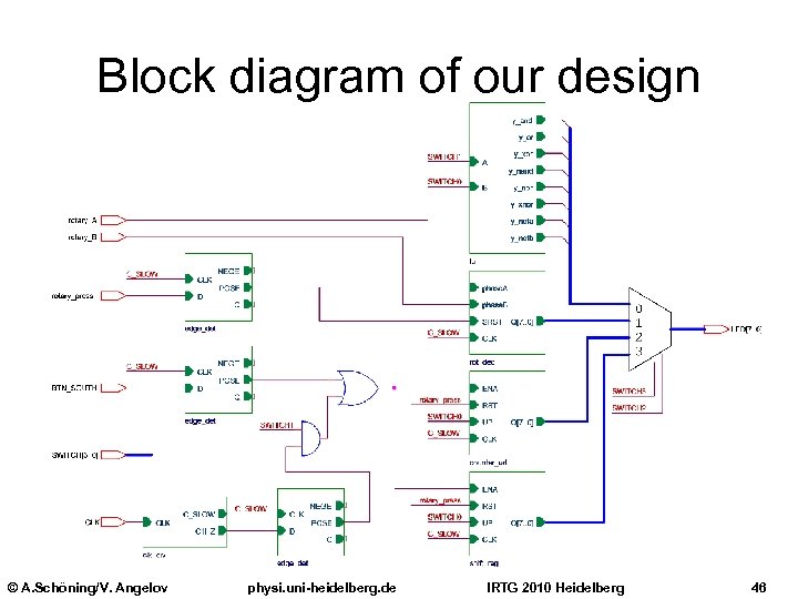 Block diagram of our design © A. Schöning/V. Angelov physi. uni-heidelberg. de IRTG 2010 Heidelberg 46
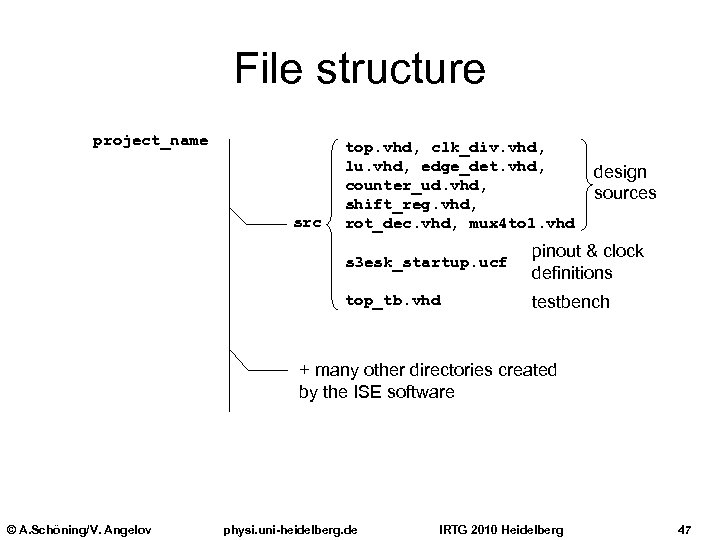 File structure project_name src top. vhd, clk_div. vhd, lu. vhd, edge_det. vhd, counter_ud. vhd, shift_reg. vhd, rot_dec. vhd, mux 4 to 1. vhd design sources s 3 esk_startup. ucf pinout & clock definitions top_tb. vhd testbench + many other directories created by the ISE software © A. Schöning/V. Angelov physi. uni-heidelberg. de IRTG 2010 Heidelberg 47
 First steps with ISE • • • Create new design Add the prepared sources to the design Edit the proper source file(s) Compile the project Program the FPGA on the board and test your design! • Simulate 1) behaviour; 2) post-route © A. Schöning/V. Angelov physi. uni-heidelberg. de IRTG 2010 Heidelberg 48
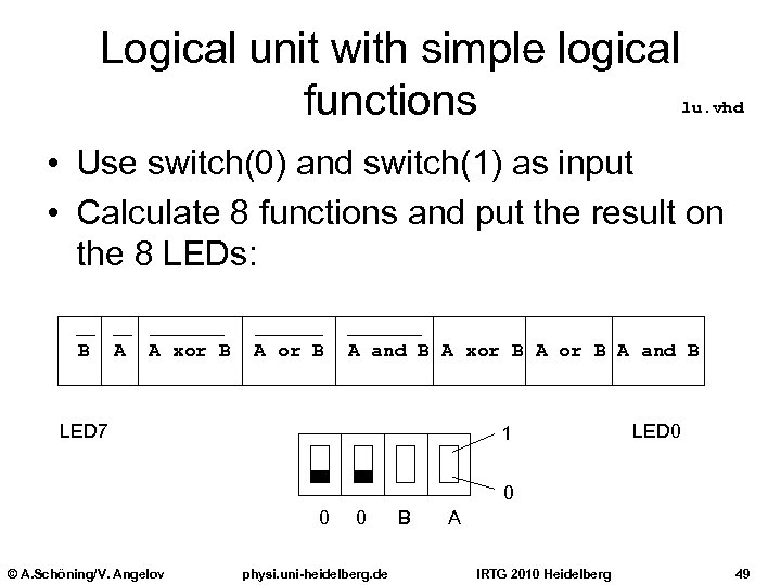 Logical unit with simple logical functions lu. vhd • Use switch(0) and switch(1) as input • Calculate 8 functions and put the result on the 8 LEDs: B A A xor B A and B LED 7 1 LED 0 0 0 © A. Schöning/V. Angelov 0 physi. uni-heidelberg. de B A IRTG 2010 Heidelberg 49
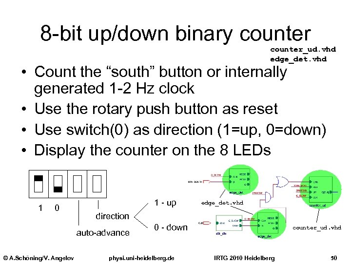 8 -bit up/down binary counter_ud. vhd edge_det. vhd • Count the “south” button or internally generated 1 -2 Hz clock • Use the rotary push button as reset • Use switch(0) as direction (1=up, 0=down) • Display the counter on the 8 LEDs 1 0 1 - up direction auto-advance © A. Schöning/V. Angelov edge_det. vhd 0 - down physi. uni-heidelberg. de counter_ud. vhd IRTG 2010 Heidelberg 50
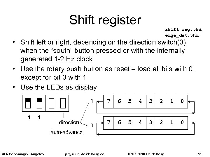 Shift register shift_reg. vhd edge_det. vhd • Shift left or right, depending on the direction switch(0) when the “south” button pressed or with the internally generated 1 -2 Hz clock • Use the rotary push button as reset – load all bits with 0, except for bit 0 with 1 • Use the LEDs as display 1 1 1 direction 0 7 6 5 4 3 2 1 0 auto-advance © A. Schöning/V. Angelov physi. uni-heidelberg. de IRTG 2010 Heidelberg 51
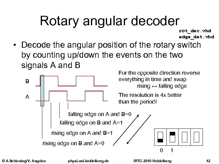 Rotary angular decoder rot_dec. vhd edge_det. vhd • Decode the angular position of the rotary switch by counting up/down the events on the two signals A and B B For the opposite direction reverse everything in time and swap rising ↔ falling edge A The resolution is 4 x better than the period! falling edge on A and B=0 rising falling edge on B and A=1 rising edge on AA and B=1 falling edge on and B=1 rising edge on BB and A=0 falling edge on and A=0 0 © A. Schöning/V. Angelov physi. uni-heidelberg. de 1 IRTG 2010 Heidelberg 52
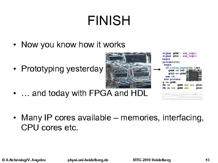 FINISH • Now you know how it works • Prototyping yesterday • … and today with FPGA and HDL signal q. NEW : std_logic; signal q. OLD : std_logic; begin process(clk) begin if rising_edge(clk) then q. NEW <= INP; q. OLD <= q. NEW; end if; end process; q <= q. NEW; RE <= q. NEW and not q. OLD; FE <= not q. NEW and q. OLD; • Many IP cores available – memories, interfacing, CPU cores etc. © A. Schöning/V. Angelov physi. uni-heidelberg. de IRTG 2010 Heidelberg 53


