88bc08366035b5d7a822ec1425c941bc.ppt
- Количество слайдов: 54
 Introduction to CMOS Process Integration
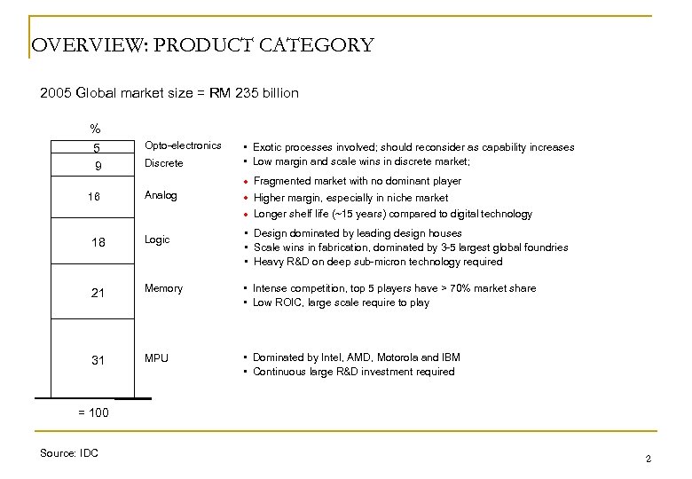 OVERVIEW: PRODUCT CATEGORY 2005 Global market size = RM 235 billion % 5 9 16 Opto-electronics Discrete Analog • Exotic processes involved; should reconsider as capability increases • Low margin and scale wins in discrete market; • • • Fragmented market with no dominant player Higher margin, especially in niche market Longer shelf life (~15 years) compared to digital technology • Design dominated by leading design houses • Scale wins in fabrication, dominated by 3 -5 largest global foundries • Heavy R&D on deep sub-micron technology required 18 Logic 21 Memory • Intense competition, top 5 players have > 70% market share • Low ROIC, large scale require to play 31 MPU • Dominated by Intel, AMD, Motorola and IBM • Continuous large R&D investment required = 100 Source: IDC 2
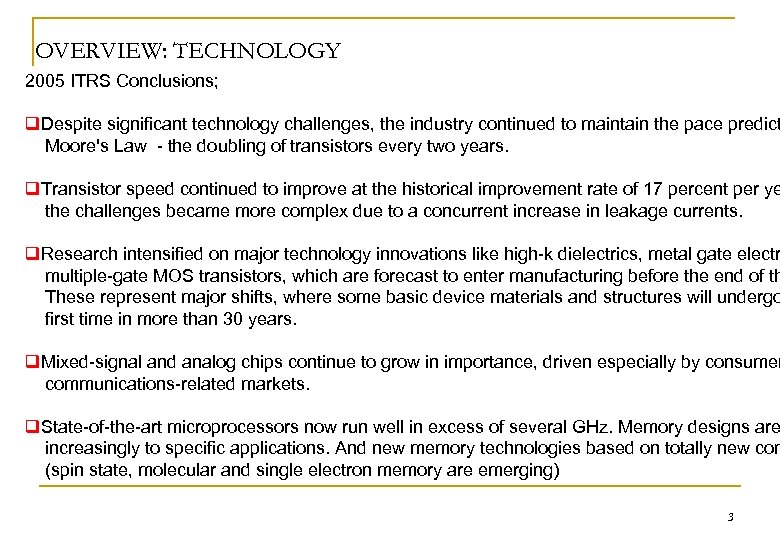 OVERVIEW: TECHNOLOGY 2005 ITRS Conclusions; q. Despite significant technology challenges, the industry continued to maintain the pace predict Moore's Law - the doubling of transistors every two years. q. Transistor speed continued to improve at the historical improvement rate of 17 percent per ye the challenges became more complex due to a concurrent increase in leakage currents. q. Research intensified on major technology innovations like high-k dielectrics, metal gate electr multiple-gate MOS transistors, which are forecast to enter manufacturing before the end of th These represent major shifts, where some basic device materials and structures will undergo first time in more than 30 years. q. Mixed-signal and analog chips continue to grow in importance, driven especially by consumer communications-related markets. q. State-of-the-art microprocessors now run well in excess of several GHz. Memory designs are increasingly to specific applications. And new memory technologies based on totally new con (spin state, molecular and single electron memory are emerging) 3
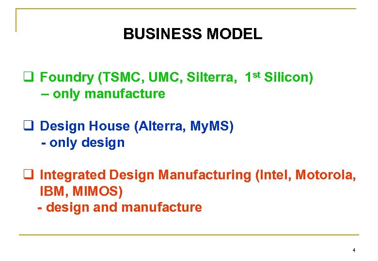 BUSINESS MODEL q Foundry (TSMC, UMC, Silterra, 1 st Silicon) – only manufacture q Design House (Alterra, My. MS) - only design q Integrated Design Manufacturing (Intel, Motorola, IBM, MIMOS) - design and manufacture 4
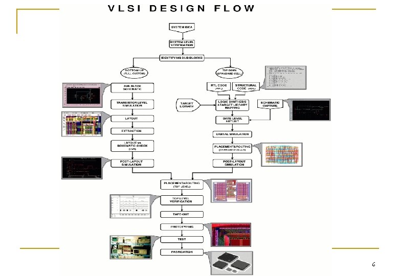
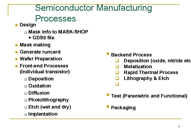 Semiconductor Manufacturing Processes n n n Design q Mask info to MASK-SHOP + GDSII file Mask making Generate runcard Wafer Preparation Front-end Processes (individual transistor) q Deposition q Oxidation q Diffusion q Photolithography q Etch (wet and dry) q Implantation § Backend Process q q q Deposition (oxide, nitride etc Metalization Rapid Thermal Process Lithography & Etch § Test (Parametric and Functional) § Packaging 5
 6
6
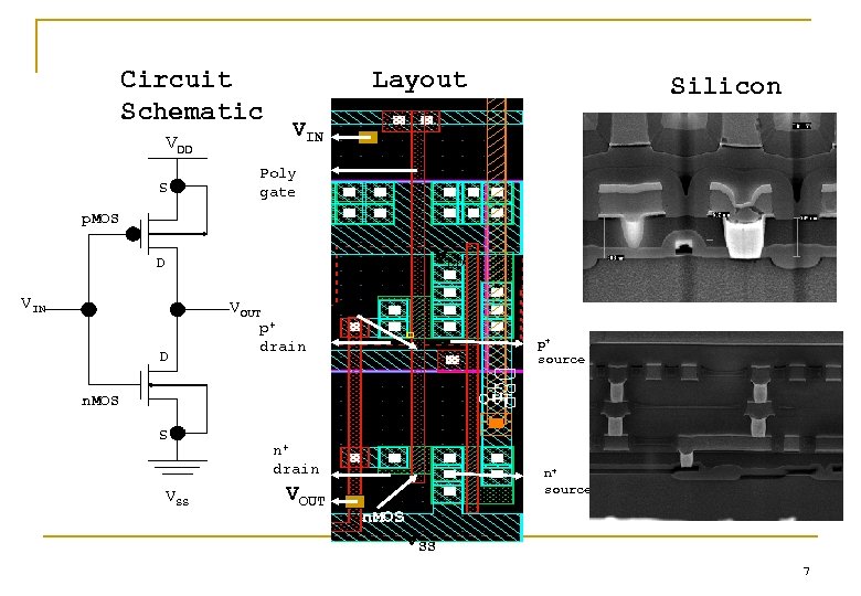 Circuit Schematic VDD S Layout Silicon VIN Poly gate p. MOS v. DD D VIN p. MOS VOUT D p+ drain p+ source n. MOS S VSS n+ drain VOUT n+ source n. MOS v. SS 7
 SILICON COMPONENTS FOR INTEGRATION • Contacts • Resistors • Capacitors • P-N Junctions • Bipolar Transistors • Uni-polar Transistor (FET) 8
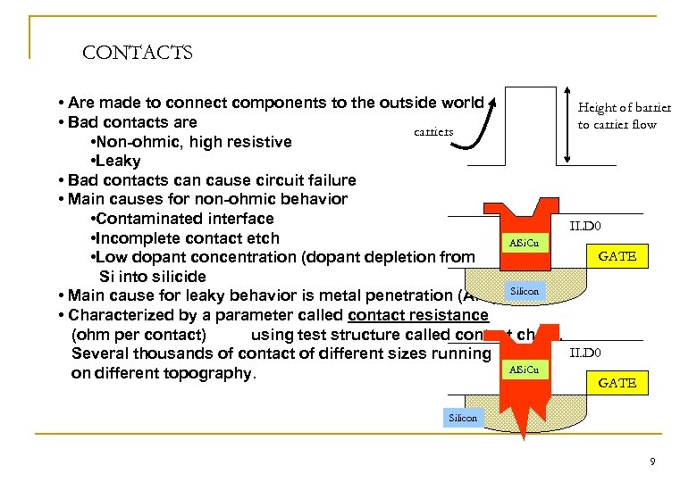 CONTACTS • Are made to connect components to the outside world • Bad contacts are carriers • Non-ohmic, high resistive • Leaky • Bad contacts can cause circuit failure • Main causes for non-ohmic behavior • Contaminated interface • Incomplete contact etch Al. Si. Cu • Low dopant concentration (dopant depletion from Si into silicide Silicon • Main cause for leaky behavior is metal penetration (Al spiking) • Characterized by a parameter called contact resistance (ohm per contact) using test structure called contact chain. Several thousands of contact of different sizes running Al. Si. Cu on different topography. Height of barrier to carrier flow ILD 0 GATE Silicon 9
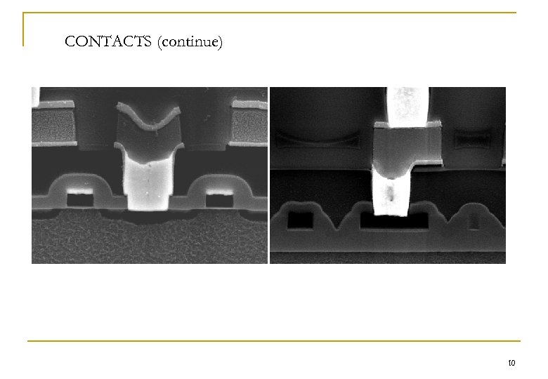 CONTACTS (continue) 10
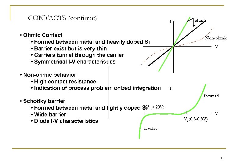 CONTACTS (continue) I • Ohmic Contact • Formed between metal and heavily doped Si • Barrier exist but is very thin • Carriers tunnel through the carrier • Symmetrical I-V characteristics • Non-ohmic behavior • High contact resistance • Indication of process problem or bad integration • Schottky barrier BV • Formed between metal and lightly doped Si (>20 V) • Wide barrier • Diode I-V characteristics ohmic Non-ohmic V I forward V Vt (0. 3 -0. 8 V) reverse 11
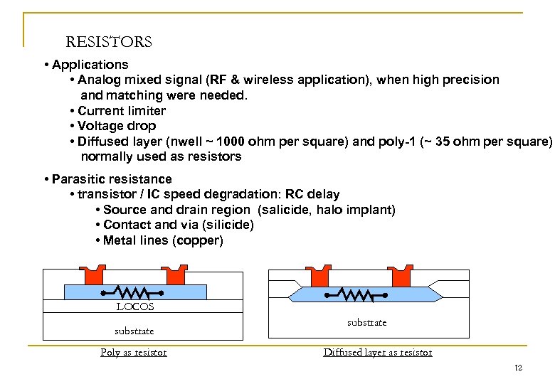 RESISTORS • Applications • Analog mixed signal (RF & wireless application), when high precision and matching were needed. • Current limiter • Voltage drop • Diffused layer (nwell ~ 1000 ohm per square) and poly-1 (~ 35 ohm per square) normally used as resistors • Parasitic resistance • transistor / IC speed degradation: RC delay • Source and drain region (salicide, halo implant) • Contact and via (silicide) • Metal lines (copper) LOCOS substrate Poly as resistor substrate Diffused layer as resistor 12
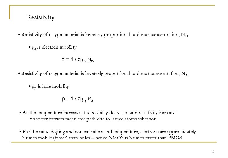 Resistivity • Resistivity of n-type material is inversely proportional to donor concentration, ND • µn is electron mobility ρ = 1 / q µn ND • Resistivity of p-type material is inversely proportional to donor concentration, NA • µp is hole mobility ρ = 1 / q µp NA • As the temperature increases, the mobility decreases and resistivity increases • shorter carriers mean free path due to lattice atoms vibration • For the same doping and concentration and temperature, electrons are approximately 3 times mobile (faster) than holes – hence NMOS is 3 times faster than PMOS 13
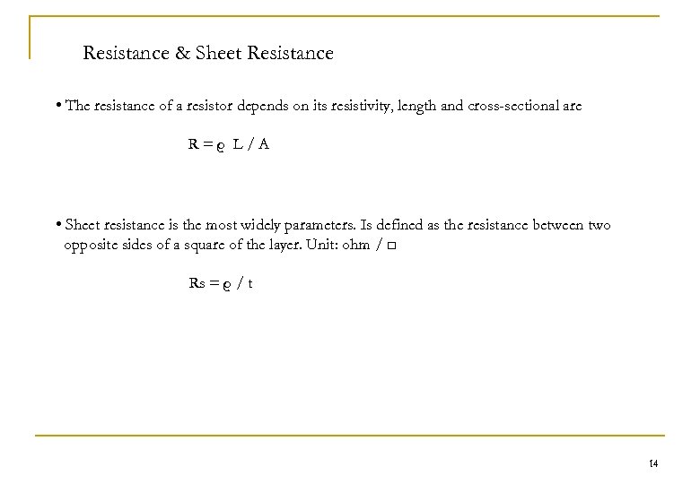 Resistance & Sheet Resistance • The resistance of a resistor depends on its resistivity, length and cross-sectional are R=ρ L/A • Sheet resistance is the most widely parameters. Is defined as the resistance between two opposite sides of a square of the layer. Unit: ohm / □ Rs = ρ / t 14
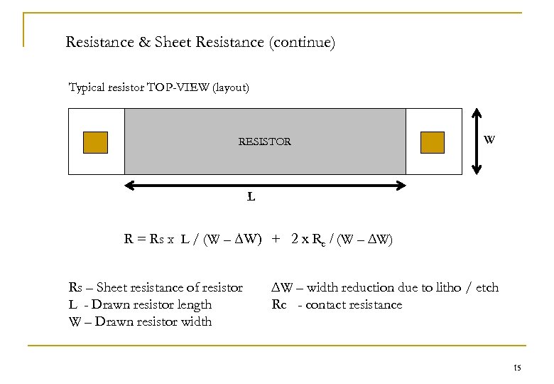 Resistance & Sheet Resistance (continue) Typical resistor TOP-VIEW (layout) RESISTOR W L R = Rs x L / (W – ΔW) + 2 x Rc / (W – ΔW) Rs – Sheet resistance of resistor L - Drawn resistor length W – Drawn resistor width ΔW – width reduction due to litho / etch Rc - contact resistance 15
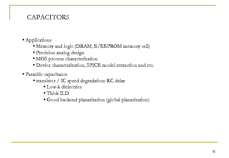 CAPACITORS • Applications • Memory and logic (DRAM, E/EEPROM memory cell) • Precision analog design • MOS process characterization • Device characterization, SPICE model extraction and etc. • Parasitic capacitance • transistor / IC speed degradation: RC delay • Low-k dielectrics • Thick ILD • Good backend planarization (global planarization) 16
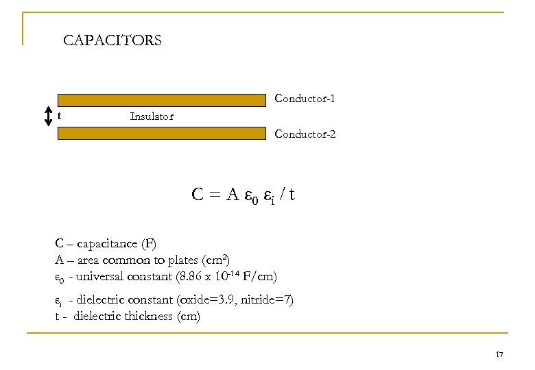 CAPACITORS Conductor-1 t Insulator Conductor-2 C = A ε 0 εi / t C – capacitance (F) A – area common to plates (cm 2) ε 0 - universal constant (8. 86 x 10 -14 F/cm) εi - dielectric constant (oxide=3. 9, nitride=7) t - dielectric thickness (cm) 17
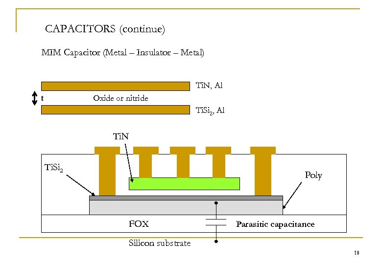 CAPACITORS (continue) MIM Capacitor (Metal – Insulator – Metal) Ti. N, Al t Oxide or nitride Ti. Si 2, Al Ti. N Ti. Si 2 Poly FOX Parasitic capacitance Silicon substrate 18
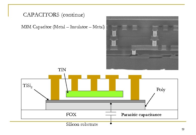 CAPACITORS (continue) MIM Capacitor (Metal – Insulator – Metal) Ti. N Ti. Si 2 Poly FOX Parasitic capacitance Silicon substrate 19
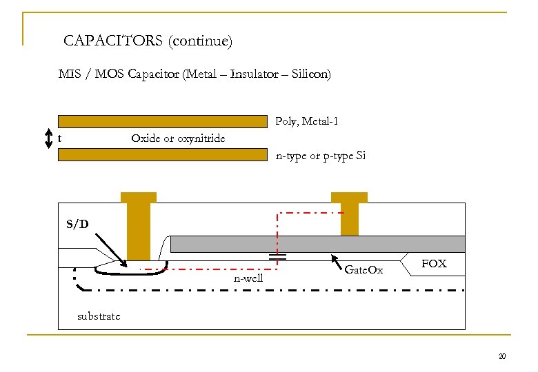 CAPACITORS (continue) MIS / MOS Capacitor (Metal – Insulator – Silicon) Poly, Metal-1 t Oxide or oxynitride n-type or p-type Si S/D n-well Gate. Ox FOX substrate 20
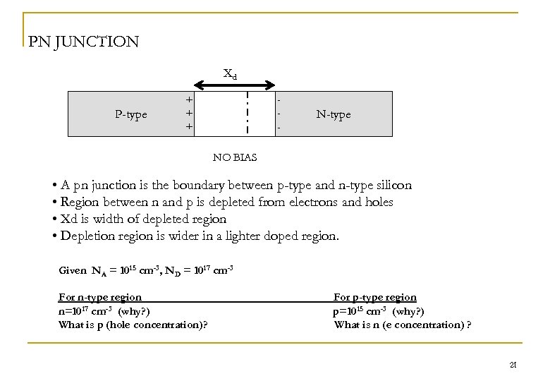 PN JUNCTION Xd P-type + + + - N-type NO BIAS • A pn junction is the boundary between p-type and n-type silicon • Region between n and p is depleted from electrons and holes • Xd is width of depleted region • Depletion region is wider in a lighter doped region. Given NA = 1015 cm-3, ND = 1017 cm-3 For n-type region n=1017 cm-3 (why? ) What is p (hole concentration)? For p-type region p=1015 cm-3 (why? ) What is n (e concentration) ? 21
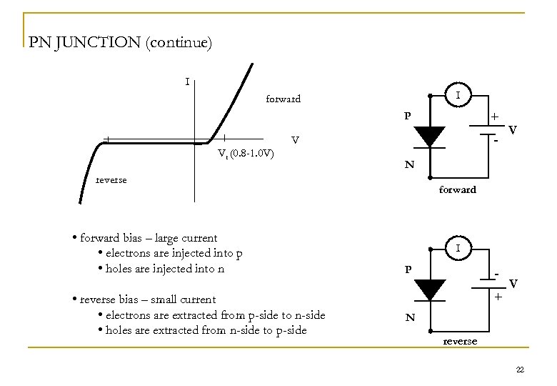 PN JUNCTION (continue) I I forward + P - V Vt (0. 8 -1. 0 V) N reverse • forward bias – large current • electrons are injected into p • holes are injected into n • reverse bias – small current • electrons are extracted from p-side to n-side • holes are extracted from n-side to p-side V forward I P + V N reverse 22
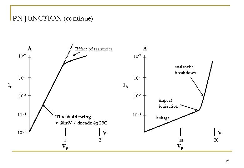 PN JUNCTION (continue) A A Effect of resistance 10 -2 avalanche breakdown 10 -5 IF IR 10 -8 10 -11 Threshold swing > 60 m. V / decade @ 25 C 10 -14 impact ionization V 1 VF 2 10 -11 leakage V 10 20 VR 23
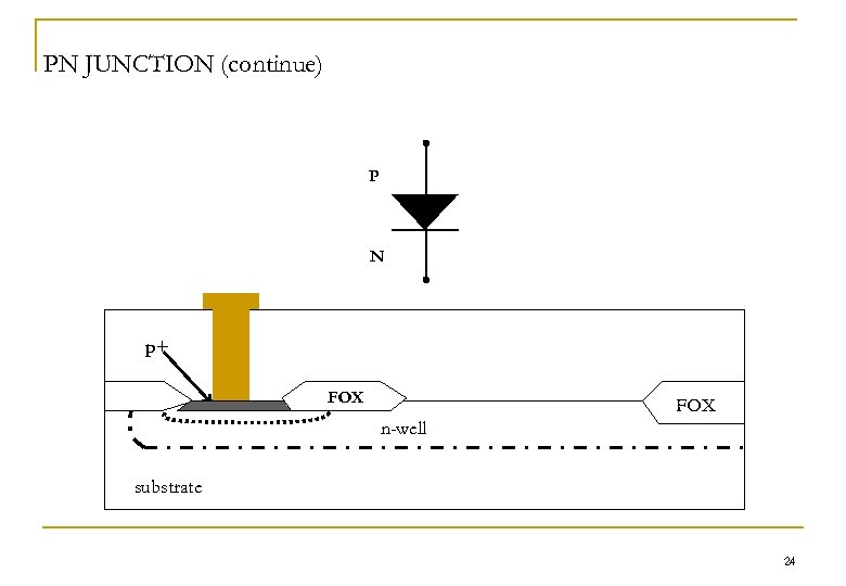 PN JUNCTION (continue) P N p+ FOX n-well substrate 24
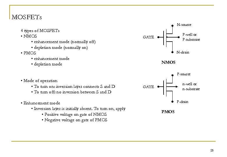 MOSFETs N-source 4 types of MOSFETs • NMOS • enhancement mode (normally off) • depletion mode (normally on) • PMOS • enhancement mode • depletion mode P-well or P-substrate GATE N-drain NMOS P-source • Mode of operation • To turn on: inversion layer connects S and D • To turn off: no inversion between S and D • Enhancement mode • Inversion layer is initially absent. To turn on, apply • Positive voltage on gate of NMOS • Negative voltage on gate of PMOS n-well or n-substrate GATE P-drain PMOS 25
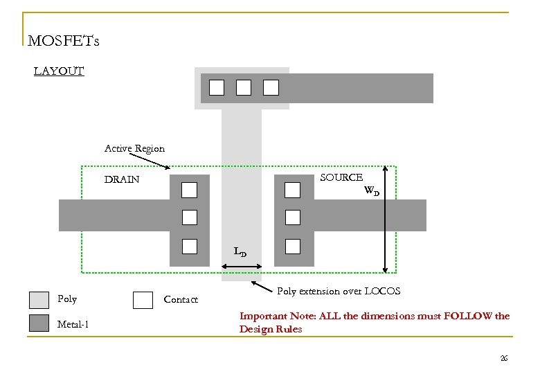 MOSFETs LAYOUT Active Region SOURCE DRAIN WD LD Poly Metal-1 Contact Poly extension over LOCOS Important Note: ALL the dimensions must FOLLOW the Design Rules 26
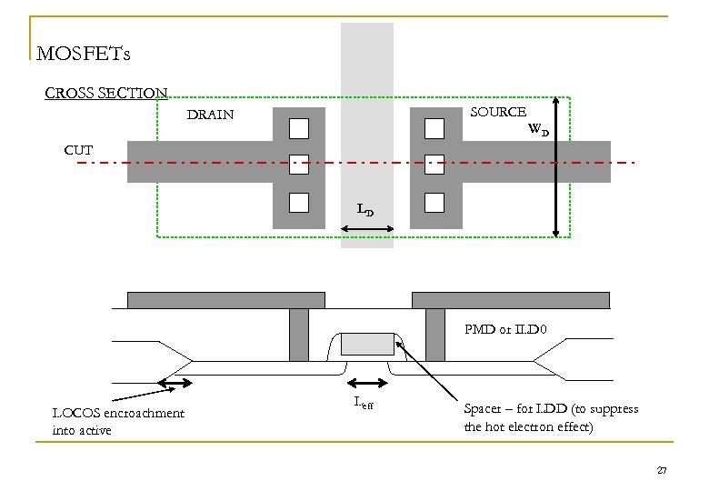 MOSFETs CROSS SECTION SOURCE DRAIN WD CUT LD PMD or ILD 0 LOCOS encroachment into active Leff Spacer – for LDD (to suppress the hot electron effect) 27
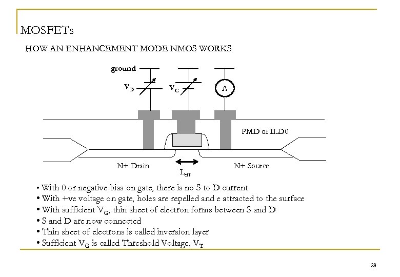 MOSFETs HOW AN ENHANCEMENT MODE NMOS WORKS ground VD VG A PMD or ILD 0 N+ Drain Leff N+ Source • With 0 or negative bias on gate, there is no S to D current • With +ve voltage on gate, holes are repelled and e attracted to the surface • With sufficient VG, thin sheet of electron forms between S and D • S and D are now connected • Thin sheet of electrons is called inversion layer • Sufficient VG is called Threshold Voltage, VT 28
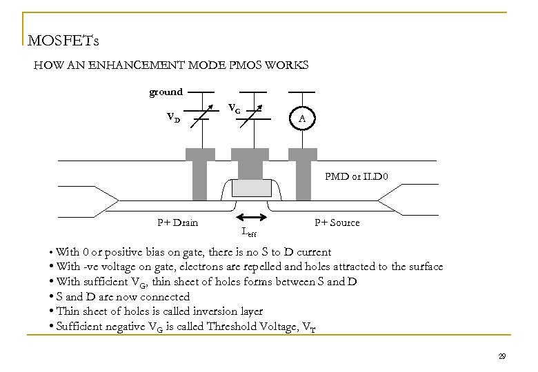 MOSFETs HOW AN ENHANCEMENT MODE PMOS WORKS ground VD VG A PMD or ILD 0 P+ Drain Leff P+ Source • With 0 or positive bias on gate, there is no S to D current • With -ve voltage on gate, electrons are repelled and holes attracted to the surface • With sufficient VG, thin sheet of holes forms between S and D • S and D are now connected • Thin sheet of holes is called inversion layer • Sufficient negative VG is called Threshold Voltage, VT 29
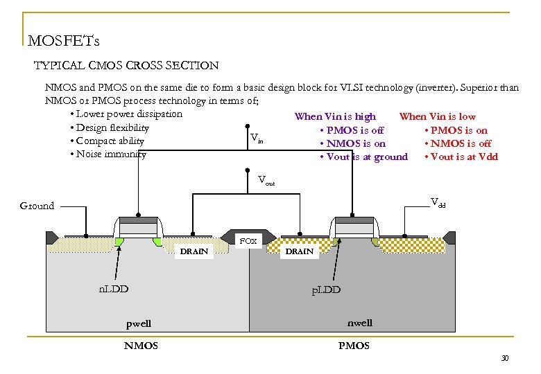 MOSFETs TYPICAL CMOS CROSS SECTION NMOS and PMOS on the same die to form a basic design block for VLSI technology (inverter). Superior than NMOS or PMOS process technology in terms of; • Lower power dissipation When Vin is high When Vin is low • Design flexibility • PMOS is off • PMOS is on Vin • Compact ability • NMOS is on • NMOS is off • Noise immunity • Vout is at ground • Vout is at Vdd Vout Vdd Ground FOX DRAIN n. LDD pwell NMOS DRAIN p. LDD nwell PMOS 30
 CMOS PROCESS INTEGRATION 31
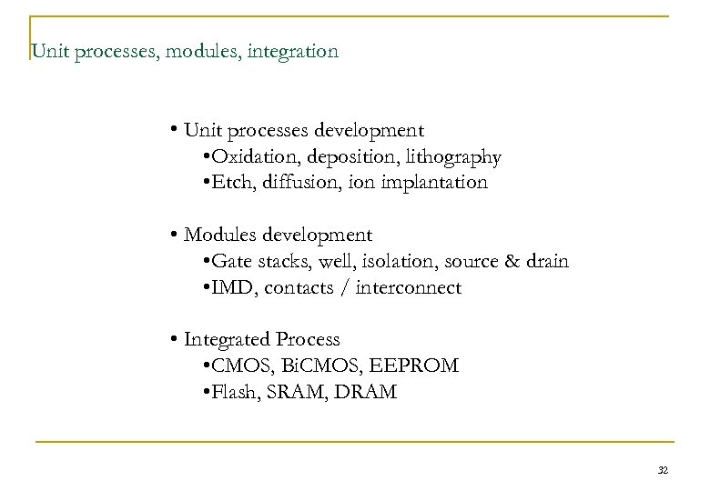 Unit processes, modules, integration • Unit processes development • Oxidation, deposition, lithography • Etch, diffusion, ion implantation • Modules development • Gate stacks, well, isolation, source & drain • IMD, contacts / interconnect • Integrated Process • CMOS, Bi. CMOS, EEPROM • Flash, SRAM, DRAM 32
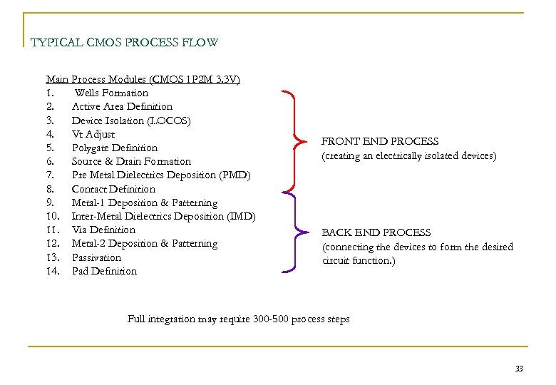 TYPICAL CMOS PROCESS FLOW Main Process Modules (CMOS 1 P 2 M 3. 3 V) 1. Wells Formation 2. Active Area Definition 3. Device Isolation (LOCOS) 4. Vt Adjust 5. Polygate Definition 6. Source & Drain Formation 7. Pre Metal Dielectrics Deposition (PMD) 8. Contact Definition 9. Metal-1 Deposition & Patterning 10. Inter-Metal Dielectrics Deposition (IMD) 11. Via Definition 12. Metal-2 Deposition & Patterning 13. Passivation 14. Pad Definition FRONT END PROCESS (creating an electrically isolated devices) BACK END PROCESS (connecting the devices to form the desired circuit function. ) Full integration may require 300 -500 process steps 33
 DEVICE ISOLATION TECHNOLOGY • Electric circuit in VLSI technology is implemented by connecting isolated devices through specific conducting path. • To fabricate monolithic ICs, electrically isolated devices must be created in the silicon substrate. • Only later they are connected. • Improper isolated device will result; • total circuit failure • high leakage (large dc power dissipation) • noise margin degradation • voltage shift, cross talk between transistors and etc. • The challenge is VLSI device only allows single transistor leakage < 10 p. A/um). On the other hand, process integration imposed a stringent requirement on the isolation technology; • spacing between actives should be as small as possible • to produce the surface topography as planar as possible • isolation process module must be simple to implement and easy to control 34
 DEVICE ISOLATION TECHNOLOGY MOS Device Isolation Characteristics MOS transistors are self isolated as long as; • The source-substrate and drain-substrate pn junctions are held at reverse bias • Reverse bias drain-substrate leakage should be negligible • Insignificant drain-source current during OFF state • Parasitic channels are prevented from forming among adjacent devices • Negligible leakage current between adjacent MOS devices 35
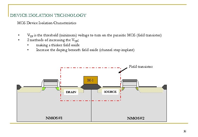 DEVICE ISOLATION TECHNOLOGY MOS Device Isolation Characteristics • • VTF is the threshold (minimum) voltage to turn on the parasitic MOS (field transistor) 2 methods of increasing the VTF; • making a thicker field oxide • Increase the doping beneath field oxide (channel stop implant) Field transistor M-1 DRAIN NMOS#1 SOURCE NMOS#2 36
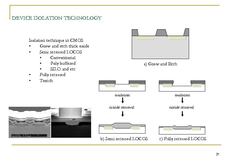 DEVICE ISOLATION TECHNOLOGY Isolation technique in CMOS • Grow and etch thick oxide • Semi recessed LOCOS • Conventional • Poly buffered • SILO and etc • Fully recessed • Trench a) Grow and Etch oxidation nitride removal b) Semi recessed LOCOS c) Fully recessed LOCOS 37
 DEVICE ISOLATION TECHNOLOGY A) Grow and etch (used until late 70 s) • • Thick oxide is grown thermally in the furnace Wafer is patterned and etch Disadvantages • • Sharp corners, difficult to cover in the latter process steps Channel stop must be implanted before oxide is grown (active to be aligned with channel stop region – low packing density) 38
 DEVICE ISOLATION TECHNOLOGY B) Semi-recessed LOCOS Conventional LOCOS • 20 -60 nm oxide is grown [pad oxide]-to cushion stress of nitride • 100 -200 nm CVD nitride is deposited as oxidation mask. Nitride is very good in this as oxygen and water vapor diffuse very slow through it. But very high tensile stress • Mask to define active regions • Channel stop implant – desirable to implant after LOCOS oxidation • Grown thick oxide using wet oxidation • Boron segregation and lateral diffusion • Bird’s beak • Strip oxide and nitride using wet etch 39
 DEVICE ISOLATION TECHNOLOGY C) Advance Semi recessed LOCOS a) • • Etch back LOCOS The simplest way to reduce bird’s beak A portion of LOCOS is etched after oxidation b) Poly buffered LOCOS • Use thinner pad oxide [poly 50 nm, oxide 10 nm] and thicker nitride • Solve the bird’s beak issue, do not solve planarization. D) Fully recessed LOCOS Quiz: Write an essay on a Fully recessed LOCOS isolation technology used in CMOS wafer fabrication process. 40
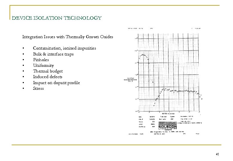 DEVICE ISOLATION TECHNOLOGY Integration Issues with Thermally Grown Oxides • • Contamination, ionized impurities Bulk & interface traps Pinholes Uniformity Thermal budget Induced defects Impact on dopant profile Stress 41
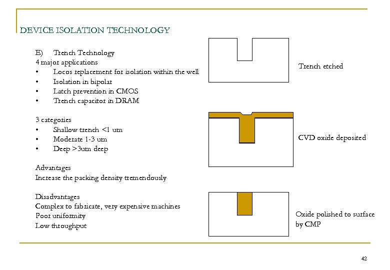 DEVICE ISOLATION TECHNOLOGY E) Trench Technology 4 major applications • Locos replacement for isolation within the well • Isolation in bipolar • Latch prevention in CMOS • Trench capacitor in DRAM 3 categories • Shallow trench <1 um • Moderate 1 -3 um • Deep >3 um deep Trench etched CVD oxide deposited Advantages Increase the packing density tremendously Disadvantages Complex to fabricate, very expensive machines Poor uniformity Low throughput Oxide polished to surface by CMP 42
 MULTI LEVEL INTERCONNECT TECHNOLOGY The requirement is to connect the device electrically at the later stages of wafer fabrication in order to implement the desired circuit functionality. 2 major components • Multilevel Metallization • Multilevel Dielectrics WHY MULTILEVEL INTERCONNECT? ? ? Contribute to ~75% low yield problem 43
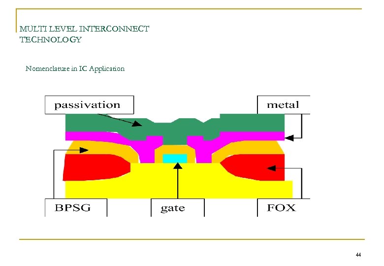 MULTI LEVEL INTERCONNECT TECHNOLOGY Nomenclature in IC Application 44
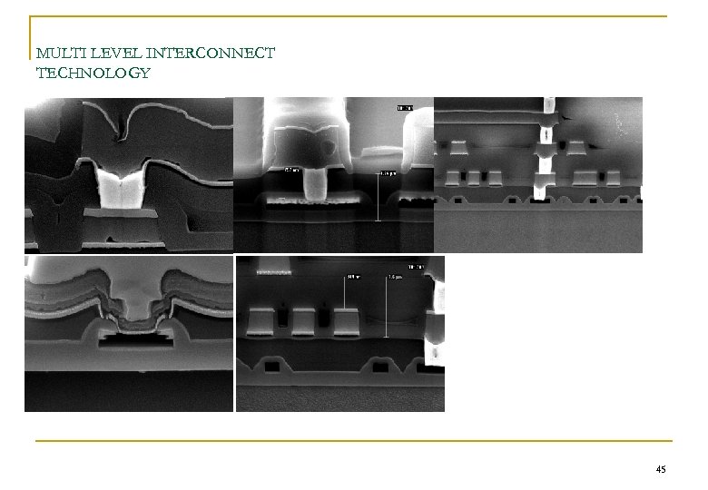 MULTI LEVEL INTERCONNECT TECHNOLOGY 45
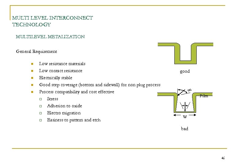 MULTI LEVEL INTERCONNECT TECHNOLOGY MULTILEVEL METALIZATION General Requirement n n n Low resistance materials Low contact resistance Electrically stable Good step coverage (bottom and sidewall) for non plug process Process compatibility and cost effective q Stress q Adhesion to oxide q Electro migration q Easiness to pattern and etch good Film W bad 46
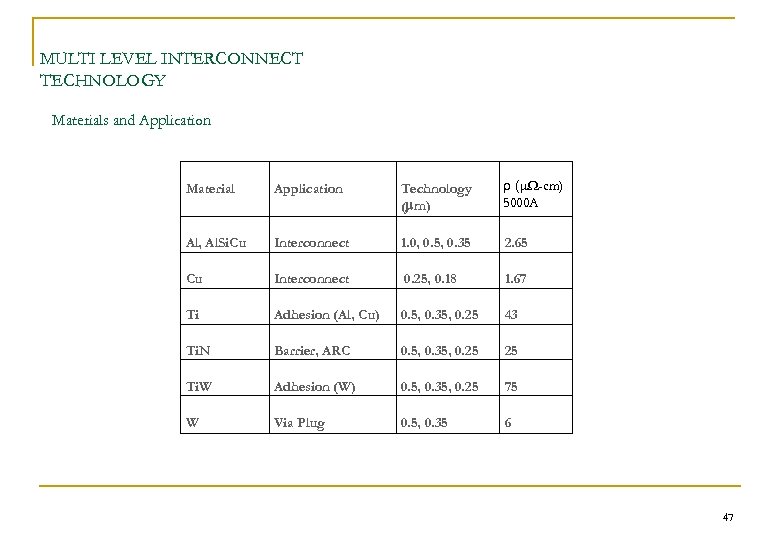 MULTI LEVEL INTERCONNECT TECHNOLOGY Materials and Application Material Application Technology ( m) ρ ( -cm) 5000 A Al, Al. Si. Cu Interconnect 1. 0, 0. 5, 0. 35 2. 65 Cu Interconnect 0. 25, 0. 18 1. 67 Ti Adhesion (Al, Cu) 0. 5, 0. 35, 0. 25 43 Ti. N Barrier, ARC 0. 5, 0. 35, 0. 25 25 Ti. W Adhesion (W) 0. 5, 0. 35, 0. 25 75 W Via Plug 0. 5, 0. 35 6 47
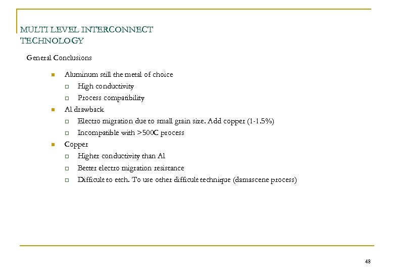 MULTI LEVEL INTERCONNECT TECHNOLOGY General Conclusions n n n Aluminum still the metal of choice q High conductivity q Process compatibility Al drawback q Electro migration due to small grain size. Add copper (1 -1. 5%) q Incompatible with >500 C process Copper q Higher conductivity than Al q Better electro migration resistance q Difficult to etch. To use other difficult technique (damascene process) 48
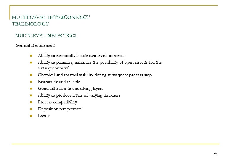 MULTI LEVEL INTERCONNECT TECHNOLOGY MULTILEVEL DIELECTRICS General Requirement n n n n n Ability to electrically isolate two levels of metal Ability to planarise, minimize the possibility of open circuits for the subsequent metal Chemical and thermal stability during subsequent process step Repeatable and reliable Good adhesion to underlying layers Ability to produce layers of varying thickness Process compatibility Deposition temperature Low k 49
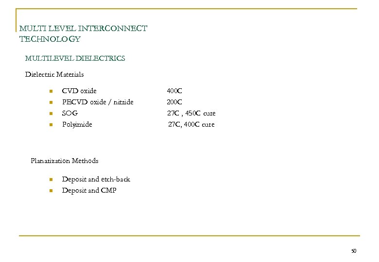 MULTI LEVEL INTERCONNECT TECHNOLOGY MULTILEVEL DIELECTRICS Dielectric Materials n n CVD oxide PECVD oxide / nitride SOG Polyimide 400 C 27 C , 450 C cure 27 C, 400 C cure Planarization Methods n n Deposit and etch-back Deposit and CMP 50
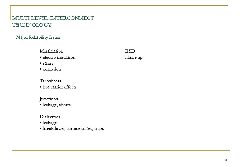 MULTI LEVEL INTERCONNECT TECHNOLOGY Major Reliability Issues Metalization • electro migration • stress • corrosion ESD Latch-up Transistors • hot carrier effects Junctions • leakage, shorts Dielectrics • leakage • breakdown, surface states, traps 51
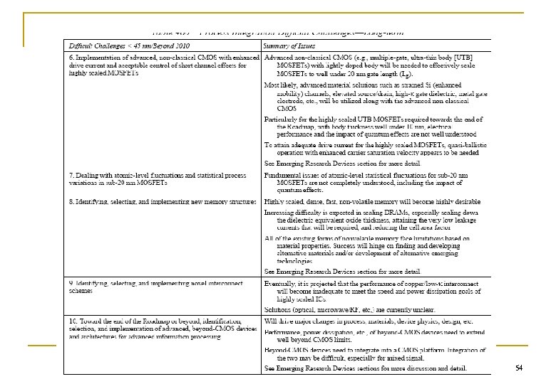
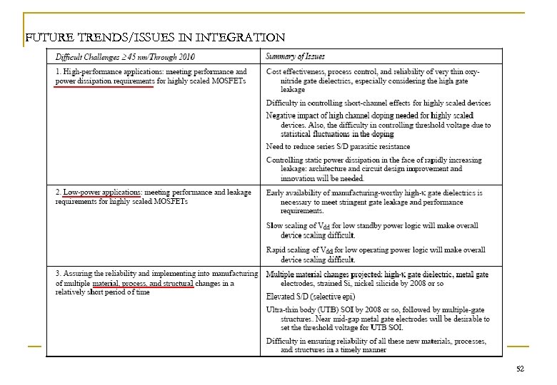 FUTURE TRENDS/ISSUES IN INTEGRATION 52
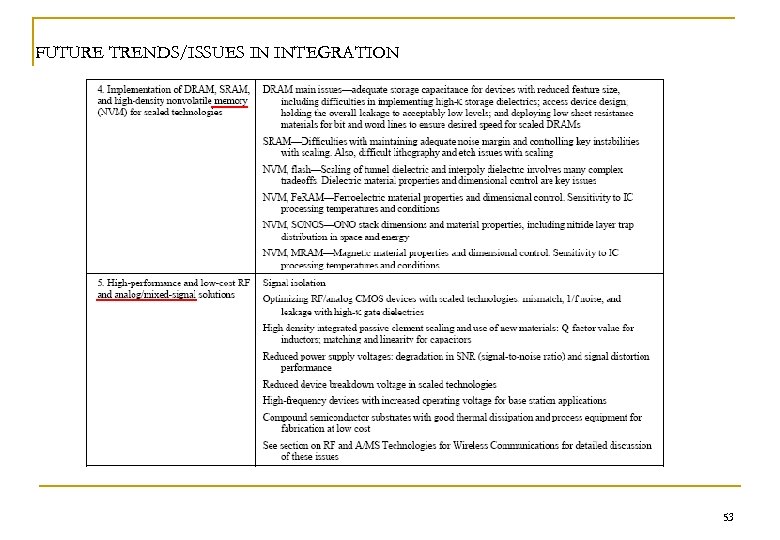 FUTURE TRENDS/ISSUES IN INTEGRATION 53
 54
54


